Product
Folder
Order
Now
Support &
Community
Tools &
Software
Technical
Documents
TCA9406
SCPS221G – OCTOBER 2010 – REVISED NOVEMBER 2018
TCA9406 2-Bit Bidirectional 1-MHz, I2C Bus and SMBus Voltage-Level Translator With
8-kV HBM ESD
1 Features
3 Description
•
The TCA9406 is a 2-bit bidirectional I2C and SMBus
voltage-level translator with an output enable (OE)
input. It is operational from 1.65 V to 3.6 V on the Aside, referenced toVCCA, and from 2.3 V to 5.5 V on
the B-side, referenced to VCCB. This allows the device
to interface between lower and higher logic signal
levels at any of the typical 1.8-V, 2.5-V, 3.3-V, and
5-V supply rails.
1
•
•
•
•
•
•
•
•
•
•
2-Bit Bidirectional Translator for SDA and SCL
Lines in I2C Applications
Provides Bidirectional Voltage Translation With No
Direction Pin
High-Impedance Output SCL_A, SDA_A, SCL_B,
SDA_B Pins When OE = Low or VCC = 0 V
Internal 10-kΩ Pullup Resistor on All SDA and
SCL Pins
1.65 V to 3.6 V on A port and 2.3 V to 5.5 V on B
port (VCCA ≤ VCCB)
VCC Isolation Feature: If Either VCC Input Is at
GND, Both Ports Are in the High-Impedance State
No Power-Supply Sequencing Required: Either
VCCA or VCCB Can Be Ramped First
Low Ioff of 2 µA When Either VCCA or VCCB = 0 V
OE Input Can Be Tied Directly to VCCA Or
Controlled By GPIO
Latch-Up Performance Exceeds 100 mA Per
JESD 78, Class II
ESD Protection Exceeds JESD 22
– A Port
– 2500-V Human-Body Model (A114-B)
– 250-V Machine Model (A115-A)
– 1500-V Charged-Device Model (C101)
– B Port
– 8-kV Human-Body Model (A114-B)
– 250-V Machine Model (A115-A)
– 1500-V Charged-Device Model (C101)
The OE input pin is referenced to VCCA, can be tied
directly to VCCA, but it is also 5.5-V tolerant. The OE
pin can also be controlled and set to a logic low to
place all the SCL and SDA pins in a high-impedance
state, which significantly reduces the quiescent
current consumption.
Under normal I2C and SMBus operation or other
open-drain configurations, the TCA9406 can support
up to 2 Mbps; therefore, it is compatible with standard
I2C speeds where the frequency of SCL is 100 kHz
(Standard-mode), 400 kHz (Fast-mode), or 1 MHz
(Fast-mode Plus). The device can also be used as a
general purpose level translator, and when the A- and
B-side ports are both driven with push-pull devices
the TCA9406 can support up to 24 Mbps.
The TCA9406 features internal 10-kΩ pullup resistors
on SCL_A, SDA_A, SCL_B, and SDA_B. Additional
external pullup resistors can be added to the bus to
reduce the total pullup resistance and speed up rising
edges.
Device Information(1)
PART NUMBER
TCA9406
2 Applications
•
•
•
I2C/SMBus
UART
GPIO
PACKAGE
BODY SIZE (NOM)
SM8 (8)
2.95 mm × 2.80 mm
US8 (8)
2.30 mm × 2.00 mm
DSBGA (8)
1.90 mm × 0.90 mm
(1) For all available packages, see the orderable addendum at
the end of the datasheet.
Typical Application Block Diagram for TCA9406
1
An IMPORTANT NOTICE at the end of this data sheet addresses availability, warranty, changes, use in safety-critical applications,
intellectual property matters and other important disclaimers. PRODUCTION DATA.
�TCA9406
SCPS221G – OCTOBER 2010 – REVISED NOVEMBER 2018
www.ti.com
Table of Contents
1
2
3
4
5
6
Features ..................................................................
Applications ...........................................................
Description .............................................................
Revision History.....................................................
Pin Configuration and Functions .........................
Specifications.........................................................
6.1
6.2
6.3
6.4
6.5
6.6
6.7
6.8
6.9
6.10
6.11
6.12
7
1
1
1
2
5
6
Absolute Maximum Ratings ..................................... 6
ESD Ratings ............................................................ 6
Recommended Operating Conditions ...................... 7
Thermal Information .................................................. 7
Electrical Characteristics .......................................... 8
Timing Requirements (VCCA = 1.8 V ± 0.15 V) ......... 9
Timing Requirements (VCCA = 2.5 V ± 0.2 V) ........... 9
Timing Requirements (VCCA = 3.3 V ± 0.3 V) ........... 9
Switching Characteristics (VCCA = 1.8 V ± 0.15 V) . 10
Switching Characteristics (VCCA = 2.5 V ± 0.2 V) . 12
Switching Characteristics (VCCA = 3.3 V ± 0.3 V) . 14
Typical Characteristics .......................................... 15
Parameter Measurement Information ................ 16
7.1 Voltage Waveforms................................................. 17
8
Detailed Description ............................................ 18
8.1
8.2
8.3
8.4
9
Overview .................................................................
Functional Block Diagram .......................................
Feature Description.................................................
Device Functional Modes........................................
18
18
18
20
Application and Implementation ........................ 21
9.1 Application Information............................................ 21
9.2 Typical Application ................................................. 21
10 Power Supply Recommendations ..................... 23
11 Layout................................................................... 23
11.1 Layout Guidelines ................................................. 23
11.2 Layout Example .................................................... 23
12 Device and Documentation Support ................. 24
12.1
12.2
12.3
12.4
12.5
Receiving Notification of Documentation Updates
Community Resources..........................................
Trademarks ...........................................................
Electrostatic Discharge Caution ............................
Glossary ................................................................
24
24
24
24
24
13 Mechanical, Packaging, and Orderable
Information ........................................................... 24
4 Revision History
NOTE: Page numbers for previous revisions may differ from page numbers in the current version.
Changes from Revision F (October 2018) to Revision G
Page
•
Changed section title From: Pullup or Pulldown Resistors on I/O Lines To: Pullup Resistors on I/O Lines........................ 20
•
Deleted text "An external pull down..." and Equation 1 from the Detailed Design Procedure section................................. 21
•
Changed pin 1 From: To controller To: To system in Figure 13 ......................................................................................... 23
•
Changed pin 5 From: To system To: To controller in Figure 13 ......................................................................................... 23
Changes from Revision E (August 2018) to Revision F
Page
•
Changed the Functional Block Diagram ............................................................................................................................... 18
•
Changed the Enable and Disable section ............................................................................................................................ 19
Changes from Revision D (July 2018) to Revision E
•
Page
Changed the new DSBGA pinout drawing From: Bottom View to: Top View ....................................................................... 5
Changes from Revision C (December 2014) to Revision D
Page
•
Changed the updated pinout drawings .................................................................................................................................. 5
•
Changed tdis no external load MAX values From: 50 To: 200 ns in Switching Characteristics (VCCA = 1.8 V ± 0.15 V)...... 10
•
Changed tdis no external load MAX values From: 40 To: 200 ns in Switching Characteristics (VCCA = 1.8 V ± 0.15 V)...... 10
•
Changed tdis no external load MAX values From: 35 To: 200 ns in Switching Characteristics (VCCA = 1.8 V ± 0.15 V)...... 11
•
Changed tdis no external load MAX values From: 50 To: 200 ns in Switching Characteristics (VCCA = 2.5 V ± 0.2 V)........ 12
•
Changed tdis no external load MAX values From: 40 To: 200 ns in Switching Characteristics (VCCA = 1.8 V ± 0.15 V)...... 12
•
Changed tdis no external load MAX values From: 35 To: 200 ns in Switching Characteristics (VCCA = 1.8 V ± 0.15 V)...... 13
•
Changed tdis no external load MAX values From: 40 To: 200 ns in Switching Characteristics (VCCA = 1.8 V ± 0.15 V)...... 14
2
Submit Documentation Feedback
Copyright © 2010–2018, Texas Instruments Incorporated
Product Folder Links: TCA9406
�TCA9406
www.ti.com
SCPS221G – OCTOBER 2010 – REVISED NOVEMBER 2018
•
Changed tdis no external load MAX values From: 35 To: 200 ns in Switching Characteristics (VCCA = 1.8 V ± 0.15 V)...... 14
•
Changed the Parameter Measurement Information section................................................................................................. 16
Submit Documentation Feedback
Copyright © 2010–2018, Texas Instruments Incorporated
Product Folder Links: TCA9406
3
�TCA9406
SCPS221G – OCTOBER 2010 – REVISED NOVEMBER 2018
www.ti.com
Changes from Revision B (June 2013) to Revision C
•
Added Pin Configuration and Functions section, ESD Ratings table, Feature Description section, Device Functional
Modes, Application and Implementation section, Power Supply Recommendations section, Layout section, Device
and Documentation Support section, and Mechanical, Packaging, and Orderable Information section .............................. 1
Changes from Revision A (Febuary 2013) to Revision B
•
4
Page
Page
Removed ordering information table, information now located in POA ................................................................................. 1
Submit Documentation Feedback
Copyright © 2010–2018, Texas Instruments Incorporated
Product Folder Links: TCA9406
�TCA9406
www.ti.com
SCPS221G – OCTOBER 2010 – REVISED NOVEMBER 2018
5 Pin Configuration and Functions
8-PIN SM8 OR US8
(TOP VIEW)
8-PIN DSBGA
(TOP VIEW)
SDA_B
1
8
SCL_B
GND
2
7
VCCB
VCCA
3
6
OE
SDA_A
4
5
SCL_A
1
2
A
SDA_B
SCL_B
B
GND
VCCB
C
VCCA
OE
D
SDA_A
SCL_A
Not to scale
Not to scale
Pin Functions
PIN
TYPE
DESCRIPTION
NAME
DCT,
DCU
YZP
SDA_B
1
A1
I/O
GND
2
B1
GND
Ground
A-port supply voltage. 1.65 V ≤ VCCA ≤ 3.6 V and VCCA ≤ VCCB
Input/output B. Referenced to VCCB.
VCCA
3
C1
Power
SDA_A
4
D1
I/O
Input/output A. Referenced to VCCA.
SCL_A
5
D2
I/O
Input/output A. Referenced to VCCA.
OE
6
C2
Input
Output enable (active High). Pull OE low to place all outputs in 3-state mode. Referenced to
VCCA.
VCCB
7
B2
Power
B-port supply voltage. 2.3 V ≤ VCCB ≤ 5.5 V
SCL_B
8
A2
I/O
Input/output B. Referenced to VCCB.
Submit Documentation Feedback
Copyright © 2010–2018, Texas Instruments Incorporated
Product Folder Links: TCA9406
5
�TCA9406
SCPS221G – OCTOBER 2010 – REVISED NOVEMBER 2018
www.ti.com
6 Specifications
6.1 Absolute Maximum Ratings (1)
over recommended operating free-air temperature range (unless otherwise noted)
VCCA
Supply voltage range
VCCB
Supply voltage range
MIN
MAX
UNIT
–0.5
4.6
V
V
–0.5
6.5
A port
–0.5
4.6
B port
–0.5
6.5
A port
–0.5
4.6
B port
–0.5
6.5
A port
–0.5
VCCA + 0.5
B port
–0.5
VCCB + 0.5
VI
Input voltage range (2)
VO
Voltage range applied to any output
in the high-impedance or power-off state (2)
VO
Voltage range applied to any output in the high or low state (2) (3)
IIK
Input clamp current
VI < 0
–50
mA
IOK
Output clamp current
VO < 0
–50
mA
IO
Continuous output current
±50
mA
±100
mA
150
°C
Continuous current through VCCA, VCCB, or GND
Tstg
(1)
(2)
(3)
Storage temperature
–65
V
V
V
Stresses beyond those listed under Absolute Maximum Ratings may cause permanent damage to the device. These are stress ratings
only, and functional operation of the device at these or any other conditions beyond those indicated under Recommended Operating
Conditions is not implied. Exposure to absolute-maximum-rated conditions for extended periods may affect device reliability.
The input and output negative-voltage ratings may be exceeded if the input and output current ratings are observed.
The value of VCCA and VCCB are provided in the recommended operating conditions table.
6.2 ESD Ratings
V(ESD)
(1)
(2)
6
Electrostatic
discharge
VALUE
UNIT
A-Port
±2500
V
B-Port
±8000
V
Charged-device model (CDM), per JEDEC specification JESD22-C101 (2)
±1500
V
Machine model (MM), A115-A
±250
V
Human-body model (HBM), per ANSI/ESDA/JEDEC JS001 (1)
JEDEC document JEP155 states that 500-V HBM allows safe manufacturing with a standard ESD control process.
JEDEC document JEP157 states that 250-V CDM allows safe manufacturing with a standard ESD control process.
Submit Documentation Feedback
Copyright © 2010–2018, Texas Instruments Incorporated
Product Folder Links: TCA9406
�TCA9406
www.ti.com
SCPS221G – OCTOBER 2010 – REVISED NOVEMBER 2018
6.3 Recommended Operating Conditions
VCCI is the supply voltage associated with the input port. VCCO is the supply voltage associated with the output port.
VCCA
VCCA
Supply voltage (1)
VCCB
Supply voltage
1.65 V to 1.95 V
A-port I/Os
High-level
input voltage
VIH
2.3 V to 3.6 V
B-port I/Os
1.65 V to 3.6 V
OE input
VCCB
2.3 V to 5.5 V
2.3 V to 5.5 V
MIN
MAX
1.65
3.6
V
2.3
5.5
V
VCCI – 0.2
VCCI
VCCI – 0.4
VCCI
VCCI – 0.4
VCCI
VCCA × 0.65
5.5
0
0.15
A-port I/Os
VIL (2)
Low-level
input voltage
B-port I/Os
1.65 V to 3.6 V
2.3 V to 5.5 V
OE input
0
0.15
0
VCCA × 0.35
A-port I/Os, pushpull driving
Δt/Δv
Input transition
rise or fall rate
TA
Operating free-air temperature
V
V
10
B-port I/Os, pushpull driving
1.65 V to 3.6 V
2.3 V to 5.5 V
10
Control input
(1)
(2)
UNIT
ns/V
10
–40
85
°C
VCCA must be less than or equal to VCCB (except during power-on transient time), and VCCA must not exceed 3.6 V.
The maximum VIL value is provided to ensure that a valid VOL is maintained. The VOL value is VIL plus the voltage drop across the passgate transistor.
6.4 Thermal Information
TCA9406
THERMAL METRIC
(1)
DCT
DCU
YZP
8 PINS
8 PINS
8 PINS
UNIT
RθJA
Junction-to-ambient thermal resistance
182.6
199.1
105.8
°C/W
RθJC(top)
Junction-to-case (top) thermal resistance
113.3
72.4
1.6
°C/W
RθJB
Junction-to-board thermal resistance
94.9
77.8
10.8
°C/W
ψJT
Junction-to-top characterization parameter
39.4
6.2
3.1
°C/W
ψJB
Junction-to-board characterization parameter
93.9
77.4
10.8
°C/W
(1)
For more information about traditional and new thermal metrics, see the Semiconductor and IC Package Thermal Metrics application
report.
Submit Documentation Feedback
Copyright © 2010–2018, Texas Instruments Incorporated
Product Folder Links: TCA9406
7
�TCA9406
SCPS221G – OCTOBER 2010 – REVISED NOVEMBER 2018
www.ti.com
6.5 Electrical Characteristics (1) (2) (3)
over recommended operating free-air temperature range (unless otherwise noted)
PARAMETER
TEST
CONDITIONS
VCCA
VCCB
VOHA
IOH = –20 μA,
VIB ≥ VCCB – 0.4 V
1.65 V to 3.6 V
2.3 V to 5.5 V
VOLA
IOL = 1 mA,
VIB ≤ 0.15 V
1.65 V to 3.6 V
2.3 V to 5.5 V
VOHB
IOH = –20 μA,
VIA ≥ VCCA – 0.2 V
1.65 V to 3.6 V
2.3 V to 5.5 V
VOLB
IOL = 1 mA,
VIA ≤ 0.15 V
1.65 V to 3.6 V
2.3 V to 5.5 V
VI = VCCI or GND
II
Ioff
IOZ
OE
8
MIN
MAX
VCCA × 0.67
UNIT
V
0.4
VCCB × 0.67
V
V
0.4
V
2.3 V to 5.5 V
±1
±2
μA
0V
0 V to 5.5 V
±1
±2
μA
B port
0 to 3.6 V
0V
±1
±2
μA
1.65 V to 3.6 V
2.3 V to 5.5 V
±1
±2
μA
1.65 V to VCCB
2.3 V to 5.5 V
2.4
3.6 V
0V
2.2
0V
5.5 V
–1
1.65 V to VCCB
2.3 V to 5.5 V
12
3.6 V
0V
–1
0V
5.5 V
1
1.65 V to VCCB
2.3 V to 5.5 V
OE
3.3 V
3.3 V
2.5
A or B port
3.3 V
3.3 V
10
A or B port
OE less than VIL
VI = VO = open,
IO = 0
VI = VO = open,
IO = 0
ICCA + ICCB
(1)
(2)
(3)
–40°C to 85°C
1.65 V to 3.6 V
ICCB
Cio
TYP
A port
ICCA
CI
TA = 25°C
VI = VO = open,
IO = 0
A port
5
6
B port
6
7.5
μA
μA
14.4
μA
3.5
pF
pF
VCCI is the VCC associated with the input port.
VCCO is the VCC associated with the output port.
VCCA must be less than or equal to VCCB, and VCCA must not exceed 3.6 V.
Submit Documentation Feedback
Copyright © 2010–2018, Texas Instruments Incorporated
Product Folder Links: TCA9406
�TCA9406
www.ti.com
SCPS221G – OCTOBER 2010 – REVISED NOVEMBER 2018
6.6 Timing Requirements (VCCA = 1.8 V ± 0.15 V)
over recommended operating free-air temperature range (unless otherwise noted)
MIN
MAX
UNIT
VCCB = 2.5 V ± 0.2 V
Data rate
tw
Pulse duration
Push-pull driving
21
Open-drain driving
Push-pull driving
Open-drain driving
2
47
Data inputs
Mbps
ns
500
VCC = 3.3 V ± 0.3 V
Data rate
tw
Pulse duration
Push-pull driving
22
Open-drain driving
Push-pull driving
Open-drain driving
2
45
Data inputs
Mbps
ns
500
VCC = 5 V ± 0.5 V
Data rate
tw
Pulse duration
Push-pull driving
24
Open-drain driving
Push-pull driving
Open-drain driving
2
41
Data inputs
Mbps
ns
500
6.7 Timing Requirements (VCCA = 2.5 V ± 0.2 V)
over recommended operating free-air temperature range (unless otherwise noted)
MIN
MAX
UNIT
VCCB = 2.5 V ± 0.2 V
Data rate
tw
Pulse duration
Push-pull driving
20
Open-drain driving
Push-pull driving
Open-drain driving
2
50
Data inputs
Mbps
ns
500
VCC = 3.3 V ± 0.3 V
Data rate
tw
Pulse duration
Push-pull driving
22
Open-drain driving
Push-pull driving
Open-drain driving
2
45
Data inputs
Mbps
ns
500
VCC = 5 V ± 0.5 V
Data rate
tw
Pulse duration
Push-pull driving
24
Open-drain driving
Push-pull driving
Open-drain driving
2
41
Data inputs
Mbps
ns
500
6.8 Timing Requirements (VCCA = 3.3 V ± 0.3 V)
over recommended operating free-air temperature range (unless otherwise noted)
MIN
MAX
UNIT
VCC = 3.3 V ± 0.3 V
Data rate
tw
Pulse duration
Push-pull driving
23
Open-drain driving
Push-pull driving
Open-drain driving
2
Data inputs
43
Mbps
ns
500
VCC = 5 V ± 0.5 V
Data rate
tw
Pulse duration
Push-pull driving
24
Open-drain driving
Push-pull driving
Open-drain driving
2
Data inputs
41
500
Mbps
ns
Submit Documentation Feedback
Copyright © 2010–2018, Texas Instruments Incorporated
Product Folder Links: TCA9406
9
�TCA9406
SCPS221G – OCTOBER 2010 – REVISED NOVEMBER 2018
www.ti.com
6.9 Switching Characteristics (VCCA = 1.8 V ± 0.15 V)
over recommended operating free-air temperature range (unless otherwise noted)
PARAMETER
FROM
(INPUT)
TO
(OUTPUT)
TEST CONDITIONS
MIN
MAX
UNIT
VCCB = 2.5 V ± 0.2 V
Push-pull driving
tPHL
A
B
tPLH
tPHL
B
A
ten
OE
A or B
tdis
OE
A or B
tPLH
Open-drain driving
5.3
2.3
Push-pull driving
6.8
Open-drain driving
50
Push-pull driving
4.4
Open-drain driving
1.9
Push-pull driving
A-port rise time
trB
B-port rise time
tfA
A-port fall time
tfB
tSK(O)
ns
5.3
ns
with external load
200
ns
no external load
200
ns
Push-pull driving
9.5
38
Push-pull driving
Open-drain driving
165
10.8
34
Push-pull driving
145
6.9
Push-pull driving
13.8
Open-drain driving
13.8
Channel-to-channel skew
0.7
Push-pull driving
Open-drain driving
ns
ns
5.9
Open-drain driving
Max data rate
ns
200
Open-drain driving
B-port fall time
5.3
5.3
Open-drain driving
trA
8.8
21
ns
ns
Mbps
2
VCCB = 3.3 V ± 0.3 V
Push-pull driving
tPHL
A
B
tPLH
tPHL
B
A
OE
A or B
tPLH
5.4
2.4
Push-pull driving
tdis
OE
A or B
trA
A-port rise time
trB
B-port rise time
tfA
A-port fall time
tfB
B-port fall time
tSK(O)
Open-drain driving
40
Push-pull driving
4.5
Open-drain driving
1.1
Push-pull driving
4.4
4.5
ns
ns
4.5
200
ns
with external load
200
ns
no external load
200
ns
Push-pull driving
9.3
Open-drain driving
30
132
23
106
Push-pull driving
Open-drain driving
9.1
Push-pull driving
6
Open-drain driving
6.4
Push-pull driving
16.2
Open-drain driving
16.2
Channel-to-channel skew
Max data rate
9.6
7.1
Open-drain driving
ten
10
Open-drain driving
0.7
Push-pull driving
Open-drain driving
Submit Documentation Feedback
22
2
ns
ns
ns
ns
ns
Mbps
Copyright © 2010–2018, Texas Instruments Incorporated
Product Folder Links: TCA9406
�TCA9406
www.ti.com
SCPS221G – OCTOBER 2010 – REVISED NOVEMBER 2018
Switching Characteristics (VCCA = 1.8 V ± 0.15 V) (continued)
over recommended operating free-air temperature range (unless otherwise noted)
PARAMETER
FROM
(INPUT)
TO
(OUTPUT)
TEST CONDITIONS
MIN
MAX
UNIT
VCCB = 5 V ± 0.5 V
Push-pull driving
tPHL
A
B
tPLH
tPHL
B
A
OE
A or B
tPLH
ten
tdis
6.8
2.6
Push-pull driving
OE
A or B
A-port rise time
trB
B-port rise time
tfA
A-port fall time
tfB
B-port fall time
Open-drain driving
33
Push-pull driving
4.7
Open-drain driving
1.2
Push-pull driving
4
0.5
ns
ns
0.5
200
ns
with external load
200
ns
no external load
200
ns
Push-pull driving
7.6
Open-drain driving
22
Push-pull driving
Open-drain driving
95
7.6
10
Push-pull driving
58
13.3
Open-drain driving
6.1
Push-pull driving
16.2
Open-drain driving
16.2
Channel-to-channel skew
Max data rate
10
7.5
Open-drain driving
trA
tSK(O)
Open-drain driving
0.7
Push-pull driving
Open-drain driving
24
2
Submit Documentation Feedback
Copyright © 2010–2018, Texas Instruments Incorporated
Product Folder Links: TCA9406
ns
ns
ns
ns
ns
Mbps
11
�TCA9406
SCPS221G – OCTOBER 2010 – REVISED NOVEMBER 2018
www.ti.com
6.10 Switching Characteristics (VCCA = 2.5 V ± 0.2 V)
over recommended operating free-air temperature range (unless otherwise noted)
PARAMETER
FROM
(INPUT)
TO
(OUTPUT)
TEST CONDITIONS
MIN
MAX
UNIT
VCCB = 2.5 V ± 0.2 V
Push-pull driving
tPHL
A
B
tPLH
Open-drain driving
3.2
1.7
3.5
Open-drain driving
3.5
Push-pull driving
tPHL
B
A
ten
OE
A or B
tdis
OE
A or B
tPLH
Open-drain driving
A-port rise time
trB
B-port rise time
tfA
A-port fall time
tfB
Push-pull driving
tSK(O)
4.7
2.5
2.5
ns
with external load
200
ns
no external load
200
ns
Push-pull driving
7.4
34
149
35
151
Push-pull driving
Open-drain driving
8.3
Push-pull driving
5.7
Open-drain driving
6.9
Push-pull driving
7.8
Open-drain driving
8.8
Channel-to-channel skew
0.7
Push-pull driving
Max data rate
ns
200
Open-drain driving
B-port fall time
ns
3
1.8
Open-drain driving
trA
6.3
Push-pull driving
Open-drain driving
20
ns
ns
ns
ns
Mbps
2
VCCB = 3.3 V ± 0.3 V
Push-pull driving
tPHL
A
B
tPLH
3.7
2
B
A
OE
A or B
tPLH
4.1
Open-drain driving
4.1
Open-drain driving
tdis
OE
A or B
trA
A-port rise time
trB
B-port rise time
tfA
A-port fall time
tfB
B-port fall time
tSK(O)
Push-pull driving
4.2
1.6
ns
1.6
200
ns
with external load
200
ns
no external load
200
ns
Push-pull driving
6.6
Open-drain driving
28
121
24
112
Push-pull driving
Open-drain driving
7.2
Push-pull driving
5.5
Open-drain driving
6.2
Push-pull driving
6.7
Open-drain driving
9.4
Channel-to-channel skew
Max data rate
ns
3.6
2.6
Open-drain driving
ten
6
Push-pull driving
Push-pull driving
tPHL
12
Open-drain driving
0.7
Push-pull driving
Open-drain driving
Submit Documentation Feedback
22
2
ns
ns
ns
ns
ns
Mbps
Copyright © 2010–2018, Texas Instruments Incorporated
Product Folder Links: TCA9406
�TCA9406
www.ti.com
SCPS221G – OCTOBER 2010 – REVISED NOVEMBER 2018
Switching Characteristics (VCCA = 2.5 V ± 0.2 V) (continued)
over recommended operating free-air temperature range (unless otherwise noted)
PARAMETER
FROM
(INPUT)
TO
(OUTPUT)
TEST CONDITIONS
MIN
MAX
UNIT
VCCB = 5 V ± 0.5 V
Push-pull driving
tPHL
A
B
tPLH
B
A
OE
A or B
tPLH
tdis
OE
A or B
A-port rise time
trB
B-port rise time
tfA
A-port fall time
tfB
B-port fall time
4.4
Open-drain driving
4.4
Open-drain driving
ns
4.3
1.2
Push-pull driving
4
1
ns
1
200
ns
with external load
200
ns
no external load
200
ns
Push-pull driving
5.6
Open-drain driving
24
Push-pull driving
Open-drain driving
89
6.1
12
64
Push-pull driving
5.3
Open-drain driving
5.8
Push-pull driving
6.6
Open-drain driving
10.4
Channel-to-channel skew
Max data rate
5.8
Push-pull driving
Open-drain driving
trA
tSK(O)
3.8
2.1
Push-pull driving
tPHL
ten
Open-drain driving
0.7
Push-pull driving
Open-drain driving
24
2
Submit Documentation Feedback
Copyright © 2010–2018, Texas Instruments Incorporated
Product Folder Links: TCA9406
ns
ns
ns
ns
ns
Mbps
13
�TCA9406
SCPS221G – OCTOBER 2010 – REVISED NOVEMBER 2018
www.ti.com
6.11 Switching Characteristics (VCCA = 3.3 V ± 0.3 V)
over recommended operating free-air temperature range (unless otherwise noted)
PARAMETER
FROM
(INPUT)
TO
(OUTPUT)
TEST CONDITIONS
MIN
MAX
UNIT
VCCB = 3.3 V ± 0.3 V
Push-pull driving
tPHL
A
B
tPLH
Open-drain driving
2.4
1.3
4.2
Open-drain driving
4.2
Push-pull driving
tPHL
B
A
ten
OE
A or B
tdis
OE
A or B
tPLH
Open-drain driving
A-port rise time
trB
B-port rise time
tfA
A-port fall time
tfB
B-port fall time
tSK(O)
Push-pull driving
124
2.5
ns
2.5
200
ns
with external load
200
ns
no external load
200
ns
Push-pull driving
5.6
Open-drain driving
25
116
26
116
Push-pull driving
Open-drain driving
6.4
Push-pull driving
5.4
Open-drain driving
6.1
Push-pull driving
7.4
Open-drain driving
7.6
Channel-to-channel skew
0.7
Push-pull driving
Max data rate
ns
2.5
1
Open-drain driving
trA
4.2
Push-pull driving
Open-drain driving
23
ns
ns
ns
ns
ns
Mbps
2
VCCB = 5 V ± 0.5 V
Push-pull driving
tPHL
A
B
tPLH
3.1
1.4
B
A
OE
A or B
tPLH
4.4
Open-drain driving
4.4
Open-drain driving
tdis
OE
A or B
trA
A-port rise time
trB
B-port rise time
tfA
A-port fall time
tfB
B-port fall time
tSK(O)
Push-pull driving
97
2.6
ns
2.6
200
ns
with external load
200
ns
no external load
200
ns
Push-pull driving
4.8
Open-drain driving
19
Push-pull driving
Open-drain driving
85
7.4
14
Push-pull driving
72
5
Open-drain driving
5.7
Push-pull driving
7.6
Open-drain driving
8.3
Channel-to-channel skew
Max data rate
ns
3.3
1
Open-drain driving
ten
4.6
Push-pull driving
Push-pull driving
tPHL
14
Open-drain driving
0.7
Push-pull driving
Open-drain driving
Submit Documentation Feedback
24
2
ns
ns
ns
ns
ns
Mbps
Copyright © 2010–2018, Texas Instruments Incorporated
Product Folder Links: TCA9406
�TCA9406
www.ti.com
SCPS221G – OCTOBER 2010 – REVISED NOVEMBER 2018
700
700
600
600
Low-Level Output Voltage (mV)
Low-Level Output Voltage (mV)
6.12 Typical Characteristics
500
400
300
200
VCCB = 2.7 V
VCCB = 3.3 V
VCCB = 5 V
100
0
0
2
VCCA = 1.8 V
4
6
8
10
12
Low-Level Current (mA)
14
500
400
300
200
100
VCCB = 3.3 V
VCCB = 5 V
0
16
0
2
4
6
8
10
12
Low-Level Current (mA)
D001
VIL(A) = 150 mV
VCCA = 2.7 V
Figure 1. Low-Level Output Voltage (VOL(Bx)) vs Low-Level
Current (IOL(Bx))
14
16
D003
VIL(A) = 150 mV
Figure 2. Low-Level Output Voltage (VOL(Bx)) vs Low-Level
Current (IOL(Bx))
Low-Level Output Voltage (mV)
700
600
500
400
300
200
100
VCCB = 3.3 V
0
0
2
4
VCCA = 3.3 V
6
8
10
12
Low-Level Current (mA)
14
16
D002
VIL(A) = 150 mV
Figure 3. Low-Level Output Voltage (VOL(Bx)) vs Low-Level Current (IOL(Bx))
Submit Documentation Feedback
Copyright © 2010–2018, Texas Instruments Incorporated
Product Folder Links: TCA9406
15
�TCA9406
SCPS221G – OCTOBER 2010 – REVISED NOVEMBER 2018
www.ti.com
7 Parameter Measurement Information
VCCI
VCCO
DUT
IN
OUT
15 pF
1M
Figure 4. Data Rate, Pulse Duration, Propagation Delay, Output Rise-Time and Fall-Time Measurement
Using a Push-Pull Driver
VCCI
VCCO
DUT
IN
OUT
15 pF
1M
Figure 5. Data Rate, Pulse Duration, Propagation Delay, Output Rise-Time and Fall-Time Measurement
Using an Open-Drain Driver
2 × VCCO
50 k
From Output
Under Test
15 pF
S1
Open
50 k
TEST
S1
tPZL / tPLZ
2 × VCCO
tPHZ / tPZH
Open
Figure 6. Load Circuit for Enable-Time and Disable-Time Measurement
1.
2.
3.
4.
16
tPLZ and tPHZ are the same as tdis.
tPZL and tPZH are the same as ten.
VCCI is the VCC associated with the input port.
VCCO is the VCC associated with the output port.
Submit Documentation Feedback
Copyright © 2010–2018, Texas Instruments Incorporated
Product Folder Links: TCA9406
�TCA9406
www.ti.com
SCPS221G – OCTOBER 2010 – REVISED NOVEMBER 2018
Parameter Measurement Information (continued)
7.1 Voltage Waveforms
tw
VCCI
Input
VCCI
VCCI / 2
VCCI / 2
0V
Input
VCCI / 2
VCCI / 2
tPLH
0V
tPHL
VCCO / 2
Output
0.1 × VCCO
tr
Figure 7. Pulse Duration
0.9 × VCCO
VOH
VCCO / 2
VOL
tf
Figure 8. Propagation Delay Times
A. CL includes probe and jig capacitance.
B. Waveform 1 in Figure 9 is for an output with internal such that the output is high, except when OE is high (see
Figure 6). Waveform 2 in Figure 9 is for an output with conditions such that the output is low, except when OE is
high.
C. All input pulses are supplied by generators having the following characteristics: PRR≤ 10 MHz, ZO = 50 Ω, dv/dt
≥ 1 V/ns.
D. The outputs are measured one at a time, with one transition per measurement.
E. tPLZ and tPHZ are the same as tdis.
F. tPZL and tPZH are the same as ten.
G. tPLH and tPHL are the same as tpd.
H. VCCI is the VCC associated with the input port.
I.
VCCO is the VCC associated with the output port.
VCCA
VCCA / 2
OE input
VCCA / 2
0V
tPLZ
tPZL
VOH
Output
Waveform 1
S1 at 2 × VCCO
VCCO / 2
VOH × 0.1
(see Note 2)
tPHZ
tPZH
Output
Waveform 2
S1 at GND
(see Note 2)
VOL
VOH × 0.9
VOH
VCCO / 2
0V
Figure 9. Enable and Disable Times
Submit Documentation Feedback
Copyright © 2010–2018, Texas Instruments Incorporated
Product Folder Links: TCA9406
17
�TCA9406
SCPS221G – OCTOBER 2010 – REVISED NOVEMBER 2018
www.ti.com
8 Detailed Description
8.1 Overview
The TCA9406 device is a directionless voltage-level translator specifically designed for translating logic voltage
levels. The A port is able to accept I/O voltages ranging from 1.65 V to 3.6 V, while the B port can accept I/O
voltages from 2.3 V to 5.5 V. The device is a pass-gate architecture with edge-rate accelerators (one-shots) to
improve the overall data rate. 10-kΩ pullup resistors, commonly used in open-drain applications, have been
conveniently integrated so that an external resistor is not needed. When TCA9406 is disabled the internal pull up
resistors are also disabled. While this device is designed for open-drain applications which makes it ideal for I2C
and SMBus applications, the device can also translate push-pull CMOS logic outputs.
8.2 Functional Block Diagram
VCCB
VCCA
OE
One Shot
Accelerator
One Shot
Accelerator
Gate Bias
10 k
10 k
SCL_A
SCL_B
One Shot
Accelerator
One Shot
Accelerator
Gate Bias
10 k
10 k
SDA_A
SDA_B
8.3 Feature Description
8.3.1 Architecture
The TCA9406 architecture (see Figure 5) is an auto-direction-sensing based translator that does not require a
direction-control signal to control the direction of data flow from A to B or from B to A.
VCCA
VCCB
T1
One
Oneshot
shot
One
Oneshot
shot
R1
10k
T2
R2
10k
Gate Bias
A
B
N2
Figure 10. Architecture of a TCA9406 Cell
18
Submit Documentation Feedback
Copyright © 2010–2018, Texas Instruments Incorporated
Product Folder Links: TCA9406
�TCA9406
www.ti.com
SCPS221G – OCTOBER 2010 – REVISED NOVEMBER 2018
Feature Description (continued)
These two bidirectional channels independently determine the direction of data flow without a direction-control
signal. Each I/O pin is automatically reconfigured as either an input or an output, which is how this auto-direction
feature is realized.
The TCA9406 is part of TI's "Switch" type voltage translator family and employs two key circuits to enable this
voltage translation:
1) An N-channel pass-gate transistor topology that ties the A-port to the B-port
and
2) Output one-shot (O.S.) edge-rate accelerator circuitry to detect and accelerate rising edges on the A or B
ports
For bidirectional voltage translation, pullup resistors are included on the device for dc current sourcing capability.
The VGATE gate bias of the N-channel pass transistor is set at approximately one threshold voltage (VT) above
the VCC level of the low-voltage side. Data can flow in either direction without guidance from a control signal.
The O.S. rising-edge rate accelerator circuitry speeds up the output slew rate by monitoring the input edge for
transitions, helping maintain the data rate through the device. During a low-to-high signal rising edge, the O.S.
circuits turn on the PMOS transistors (T1, T2) to increase the current drive capability of the driver for
approximately 30 ns or 95% of the input edge, whichever occurs first. This edge-rate acceleration provides high
ac drive by bypassing the internal 10-kΩ pullup resistors during the low-to-high transition to speed up the signal.
The output resistance of the driver is decreased to approximately 50 Ω to 70 Ω during this acceleration phase. To
minimize dynamic ICC and the possibility of signal contention, the user should wait for the O.S. circuit to turn off
before applying a signal in the opposite direction. The worst-case duration is equal to the minimum pulse-width
number provided in the Timing Requirements section of this data sheet.
8.3.2 Input Driver Requirements
The continuous dc-current "sinking" capability is determined by the external system-level open-drain (or pushpull) drivers that are interfaced to the TCA9406 I/O pins. Since the high bandwidth of these bidirectional I/O
circuits is used to facilitate this fast change from an input to an output and an output to an input, they have a
modest dc-current "sourcing" capability of hundreds of micro-Amps, as determined by the internal 10-kΩ pullup
resistors.
The fall time (tfA, tfB) of a signal depends on the edge-rate and output impedance of the external device driving
TCA9406 data I/Os, as well as the capacitive loading on the data lines.
Similarly, the tPHL and max data rates also depend on the output impedance of the external driver. The values for
tfA, tfB, tPHL, and maximum data rates in the data sheet assume that the output impedance of the external driver is
less than 50 Ω.
8.3.3 Output Load Considerations
TI recommends careful PCB layout practices with short PCB trace lengths to avoid excessive capacitive loading
and to ensure that proper O.S. triggering takes place. PCB signal trace-lengths should be kept short enough
such that the round trip delay of any reflection is less than the one-shot duration. This improves signal integrity
by ensuring that any reflection sees a low impedance at the driver. The O.S. circuits have been designed to stay
on for approximately 30 ns. The maximum capacitance of the lumped load that can be driven also depends
directly on the one-shot duration. With very heavy capacitive loads, the one-shot can time-out before the signal is
driven fully to the positive rail. The O.S. duration has been set to best optimize trade-offs between dynamic ICC,
load driving capability, and maximum bit-rate considerations. Both PCB trace length and connectors add to the
capacitance that the TCA9406 output sees, so it is recommended that this lumped-load capacitance be
considered to avoid O.S. re-triggering, bus contention, output signal oscillations, or other adverse system-level
affects.
8.3.4 Enable and Disable
The TCA9406 has an OE input that is used to disable the device by setting OE low, which places all I/Os in the
Hi-Z state. When TCA9406 is disabled, the internal pull up resistors are also disabled meaning if no external pull
up resistors are present then the SDA/SCL lines will be left floating. The disable time (tdis) indicates the delay
between the time when OE goes low and when the outputs are disabled (Hi-Z). The enable time (ten) indicates
the amount of time the user must allow for the one-shot circuitry to become operational after OE is taken high.
Submit Documentation Feedback
Copyright © 2010–2018, Texas Instruments Incorporated
Product Folder Links: TCA9406
19
�TCA9406
SCPS221G – OCTOBER 2010 – REVISED NOVEMBER 2018
www.ti.com
Feature Description (continued)
8.3.5 Pullup Resistors on I/O Lines
Each A-port I/O has an internal 10-kΩ pullup resistor to VCCA, and each B-port I/O has an internal 10-kΩ pullup
resistor to VCCB. If a smaller value of pullup resistor is required, an external resistor must be added from the I/O
to VCCA or VCCB (in parallel with the internal 10-kΩ resistors). Adding lower value pullup resistors will effect VOL
levels, however. The internal pullups of the TCA9406 are disabled when the OE pin is low.
8.4 Device Functional Modes
The TCA9406 device has two functional modes, enabled and disabled. To disable the device set the OE input
low, which places all I/Os in a high impedance state. Setting the OE input high will enable the device.
20
Submit Documentation Feedback
Copyright © 2010–2018, Texas Instruments Incorporated
Product Folder Links: TCA9406
�TCA9406
www.ti.com
SCPS221G – OCTOBER 2010 – REVISED NOVEMBER 2018
9 Application and Implementation
NOTE
Information in the following applications sections is not part of the TI component
specification, and TI does not warrant its accuracy or completeness. TI’s customers are
responsible for determining suitability of components for their purposes. Customers should
validate and test their design implementation to confirm system functionality.
9.1 Application Information
The TCA9406 can be used to bridge the digital-switching compatibility gap between two voltage nodes to
successfully interface logic threshold levels found in electronic systems. It should be used in a point-to-point
topology for interfacing devices or systems operating at different interface voltages with one another. Its primary
target application use is for interfacing with open-drain drivers on the data I/Os such as I2C or SMBus, where the
data is bidirectional and no control signal is available.
9.2 Typical Application
Optional Resistors
1.8 V
3.3 V
0.1 PF
Master
I2C
Bus
VCCA
V
VCCB
CCB
SDA_A
SCL_A
SDA_B
SCL_B
I2C
Bus
Devices
OE
Design Notes: OE can be tied directly to 1.8 V (VCCA) to always be in ENABLE mode.
Figure 11. Typical Application Circuit
9.2.1 Design Requirements
For this design example, use the parameters listed in Table 1. And make sure the VCCA ≤ VCCB.
Table 1. Design Parameters
DESIGN PARAMETER
EXAMPLE VALUE
Input voltage range
1.65 to 3.6 V
Output voltage range
2.3 to 5.5 V
9.2.2 Detailed Design Procedure
To begin the design process, determine the following:
• Input voltage range
– Use the supply voltage of the device that is driving the TCA9406 device to determine the input voltage
range. For a valid logic high the value must exceed the VIH of the input port. For a valid logic low the value
must be less than the VIL of the input port.
• Output voltage range
– Use the supply voltage of the device that the TCA9406 device is driving to determine the output voltage
range
– The TCA9406 device has 10-kΩ internal pullup resistors. External pullup resistors can be added to reduce
the total RC of a signal trace if necessary.
Submit Documentation Feedback
Copyright © 2010–2018, Texas Instruments Incorporated
Product Folder Links: TCA9406
21
�TCA9406
SCPS221G – OCTOBER 2010 – REVISED NOVEMBER 2018
www.ti.com
9.2.3 Application Curve
Figure 12. Level-Translation of a 2.5-MHz Signal
22
Submit Documentation Feedback
Copyright © 2010–2018, Texas Instruments Incorporated
Product Folder Links: TCA9406
�TCA9406
www.ti.com
SCPS221G – OCTOBER 2010 – REVISED NOVEMBER 2018
10 Power Supply Recommendations
During operation, ensure that VCCA ≤ VCCBat all times. The sequencing of each power supply will not damage the
device during the power up operation, so either power supply can be ramped up first. The output-enable (OE)
input circuit is designed so that it is supplied by VCCA and when the (OE) input is low, all outputs are placed in the
high-impedance state. To ensure the high-impedance state of the outputs during power up or power down, the
OE input pin must be tied to GND through a pulldown resistor and must not be enabled until VCCA and VCCB are
fully ramped and stable. The minimum value of the pulldown resistor to ground is determined by the currentsourcing capability of the driver.
11 Layout
11.1 Layout Guidelines
To ensure reliability of the device, the following common printed-circuit board layout guidelines are
recommended:
• Bypass capacitors should be used on power supplies and should be placed as close as possible to the VCCA,
VCCB pin, and GND pin.
• Short trace lengths should be used to avoid excessive loading.
• PCB signal trace-lengths must be kept short enough so that the round-trip delay of any reflection is less than
the one-shot duration, approximately 30 ns, ensuring that any reflection encounters low impedance at the
source driver.
11.2 Layout Example
Legend
Via to power plane
Via to GND plane (inner layer)
TCA9406
To system
To system
1
SDA_B
SCL_B
8
2
GND
VCCB
7
Bypass capacitor
OE
6
Keep OE low until VCCA
and VCCB are powered up
SCL_A
5
0.1 F
Bypass capacitor
0.1 F
3
VCCA
4
SDA_A
To controller
To controller
Figure 13. TCA9406 Layout Example
Submit Documentation Feedback
Copyright © 2010–2018, Texas Instruments Incorporated
Product Folder Links: TCA9406
23
�TCA9406
SCPS221G – OCTOBER 2010 – REVISED NOVEMBER 2018
www.ti.com
12 Device and Documentation Support
12.1 Receiving Notification of Documentation Updates
To receive notification of documentation updates, navigate to the device product folder on ti.com. In the upper
right corner, click on Alert me to register and receive a weekly digest of any product information that has
changed. For change details, review the revision history included in any revised document.
12.2 Community Resources
The following links connect to TI community resources. Linked contents are provided "AS IS" by the respective
contributors. They do not constitute TI specifications and do not necessarily reflect TI's views; see TI's Terms of
Use.
TI E2E™ Online Community TI's Engineer-to-Engineer (E2E) Community. Created to foster collaboration
among engineers. At e2e.ti.com, you can ask questions, share knowledge, explore ideas and help
solve problems with fellow engineers.
Design Support TI's Design Support Quickly find helpful E2E forums along with design support tools and
contact information for technical support.
12.3 Trademarks
E2E is a trademark of Texas Instruments.
All other trademarks are the property of their respective owners.
12.4 Electrostatic Discharge Caution
This integrated circuit can be damaged by ESD. Texas Instruments recommends that all integrated circuits be handled with
appropriate precautions. Failure to observe proper handling and installation procedures can cause damage.
ESD damage can range from subtle performance degradation to complete device failure. Precision integrated circuits may be more
susceptible to damage because very small parametric changes could cause the device not to meet its published specifications.
12.5 Glossary
SLYZ022 — TI Glossary.
This glossary lists and explains terms, acronyms, and definitions.
13 Mechanical, Packaging, and Orderable Information
The following pages include mechanical, packaging, and orderable information. This information is the most
current data available for the designated devices. This data is subject to change without notice and revision of
this document. For browser-based versions of this data sheet, refer to the left-hand navigation.
24
Submit Documentation Feedback
Copyright © 2010–2018, Texas Instruments Incorporated
Product Folder Links: TCA9406
�PACKAGE OPTION ADDENDUM
www.ti.com
29-Nov-2018
PACKAGING INFORMATION
Orderable Device
Status
(1)
Package Type Package Pins Package
Drawing
Qty
Eco Plan
Lead/Ball Finish
MSL Peak Temp
(2)
(6)
(3)
Op Temp (°C)
Device Marking
(4/5)
TCA9406DCTR
ACTIVE
SM8
DCT
8
3000
Green (RoHS
& no Sb/Br)
CU NIPDAU
Level-1-260C-UNLIM
-40 to 85
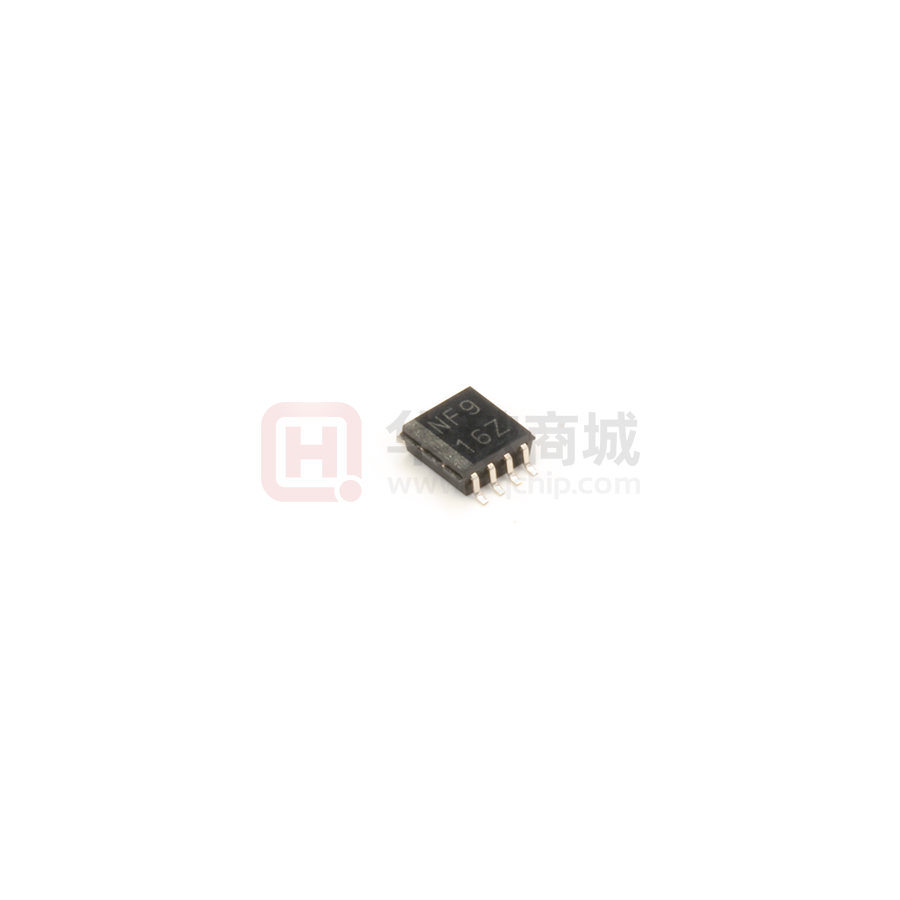
NF9
(R, Z)
TCA9406DCUR
ACTIVE
VSSOP
DCU
8
3000
Green (RoHS
& no Sb/Br)
CU NIPDAU | CU SN
Level-1-260C-UNLIM
-40 to 85
(F9, NF9R)
NZ
TCA9406YZPR
ACTIVE
DSBGA
YZP
8
3000
Green (RoHS
& no Sb/Br)
SNAGCU
Level-1-260C-UNLIM
-40 to 85
7W
(1)
The marketing status values are defined as follows:
ACTIVE: Product device recommended for new designs.
LIFEBUY: TI has announced that the device will be discontinued, and a lifetime-buy period is in effect.
NRND: Not recommended for new designs. Device is in production to support existing customers, but TI does not recommend using this part in a new design.
PREVIEW: Device has been announced but is not in production. Samples may or may not be available.
OBSOLETE: TI has discontinued the production of the device.
(2)
RoHS: TI defines "RoHS" to mean semiconductor products that are compliant with the current EU RoHS requirements for all 10 RoHS substances, including the requirement that RoHS substance
do not exceed 0.1% by weight in homogeneous materials. Where designed to be soldered at high temperatures, "RoHS" products are suitable for use in specified lead-free processes. TI may
reference these types of products as "Pb-Free".
RoHS Exempt: TI defines "RoHS Exempt" to mean products that contain lead but are compliant with EU RoHS pursuant to a specific EU RoHS exemption.
Green: TI defines "Green" to mean the content of Chlorine (Cl) and Bromine (Br) based flame retardants meet JS709B low halogen requirements of


 工商网监
湘ICP备2023018690号
工商网监
湘ICP备2023018690号

