www.ti.com
TCAN1051-Q1, TCAN1051V-Q1, TCAN1051H-Q1, TCAN1051HV-Q1
TCAN1051-Q1,
TCAN1051V-Q1,
TCAN1051H-Q1,TCAN1051HGV-Q1
TCAN1051HV-Q1
TCAN1051G-Q1,
TCAN1051GV-Q1,
TCAN1051HG-Q1,
TCAN1051G-Q1, TCAN1051GV-Q1,SLLSET0D
TCAN1051HG-Q1,
– MARCH 2016TCAN1051HGV-Q1
– REVISED APRIL 2021
SLLSET0D – MARCH 2016 – REVISED APRIL 2021
TCAN1051-Q1 Automotive Fault Protected CAN Transceiver with CAN FD
1 Features
3 Description
•
This CAN transceiver family meets the ISO11898-2
(2016) High Speed CAN (Controller Area Network)
physical layer standard. All devices are designed for
use in CAN FD networks up to 2 Mbps (megabits
per second). Devices with part numbers that include
the "G" suffix are designed for data rates up
to 5 Mbps, and versions with the "V" have a
secondary power supply input for I/O level shifting
the input pin thresholds and RXD output level. This
family of devices comes with silent mode which
is also commonly referred to as listen-only mode.
Additionally, all devices include many protection
features to enhance device and network robustness.
•
•
•
•
•
•
•
•
•
•
•
AEC Q100: Qualified for automotive applications
– Temperature grade 1: -40°C to 125°C, TA
– HBM classification level: ±16 kV
– CDM classification level ±1500 V
Meets the ISO 11898-2:2016 and
ISO 11898-5:2007 physical layer standards
Functional Safety-Capable
– Documentation available to aid functional safety
system design
'Turbo' CAN:
– All devices support classic CAN and 2 Mbps
CAN FD (flexible data rate) and "G" options
support 5 Mbps
– Short and symmetrical propagation delay times
and fast loop times for enhanced timing margin
– Higher data rates in loaded CAN networks
EMC performance: supports SAE J2962-2 and IEC
62228-3 (up to 500 kbps) without common mode
choke
I/O Voltage range supports 3.3 V and 5 V MCUs
Ideal passive behavior when unpowered
– Bus and logic terminals are high impedance (no
load)
– Power up/down with glitch free operation on
bus and RXD output
Protection features
– IEC ESD protection up to ±15 kV
– Bus Fault protection: ±58 V (non-H variants)
and ±70 V (H variants)
– Undervoltage protection on VCC and VIO (V
variants only) supply terminals
– Driver dominant time out (TXD DTO) - Data
rates down to 10 kbps
– Thermal shutdown protection (TSD)
Receiver common mode input voltage: ±30 V
Typical loop delay: 110 ns
Junction temperatures from –55°C to 150°C
Available in SOIC(8) package and leadless
VSON(8) Package (3.0 mm x 3.0 mm) with
improved automated optical inspection (AOI)
capability
Device Information
PART NUMBER
TCAN1051x-Q1
(1)
Automotive and Transportation
All devices support highly loaded CAN networks
Heavy machinery ISOBUS applications –
ISO 11783
BODY SIZE
SOIC (8)
4.90 mm × 3.91 mm
VSON (8)
3.00 mm x 3.00 mm
For all available packages, see the orderable addendum at
the end of the data sheet.
NC or VIO
VCC
5
3
VCC or VIO
TXD
1
S
8
TSD
7
CANH
Dominant
time-out
6
CANL
Mode
Select
UVP
VCC or VIO
RXD
4
Logic
Output
2
GND
A.
2 Applications
•
•
•
PACKAGE(1)
B.
Copyright © 2016, Texas Instruments Incorporated
Terminal 5 function is device dependent; NC on devices
without the "V" suffix, and VIO for I/O level shifting for devices
with the "V" suffix.
RXD logic output is driven to VCC on devices without the "V"
suffix, and VIO for devices with the "V" suffix.
Functional Block Diagram
An©IMPORTANT
NOTICEIncorporated
at the end of this data sheet addresses availability, warranty, changes, use in
safety-critical
applications,
Copyright
2021 Texas Instruments
Submit
Document
Feedback
intellectual property matters and other important disclaimers. PRODUCTION DATA.
Product Folder Links: TCAN1051-Q1 TCAN1051V-Q1 TCAN1051H-Q1 TCAN1051HV-Q1 TCAN1051G-Q1
TCAN1051GV-Q1 TCAN1051HG-Q1 TCAN1051HGV-Q1
1
�TCAN1051-Q1, TCAN1051V-Q1, TCAN1051H-Q1, TCAN1051HV-Q1
TCAN1051G-Q1, TCAN1051GV-Q1, TCAN1051HG-Q1, TCAN1051HGV-Q1
www.ti.com
SLLSET0D – MARCH 2016 – REVISED APRIL 2021
Table of Contents
1 Features............................................................................1
2 Applications..................................................................... 1
3 Description.......................................................................1
4 Revision History.............................................................. 2
5 Pin Configuration and Functions...................................5
6 Specifications.................................................................. 6
6.1 Absolute Maximum Ratings ....................................... 6
6.2 ESD Ratings............................................................... 6
6.3 ESD Ratings, Specifications....................................... 7
6.4 Recommended Operating Conditions.........................8
6.5 Thermal Information....................................................8
6.6 Power Rating.............................................................. 8
6.7 Electrical Characteristics.............................................9
6.8 Switching Characteristics..........................................12
6.9 Typical Characteristics.............................................. 13
7 Parameter Measurement Information.......................... 14
8 Detailed Description......................................................18
8.1 Overview................................................................... 18
8.2 Functional Block Diagram......................................... 18
8.3 Feature Description...................................................19
8.4 Device Functional Modes..........................................22
9 Application Information Disclaimer............................. 24
9.1 Application Information............................................. 24
9.2 Typical Applications.................................................. 24
10 Power Supply Recommendations..............................28
11 Device and Documentation Support..........................31
11.1 Documentation Support.......................................... 31
11.2 Receiving Notification of Documentation Updates.. 31
11.3 Support Resources................................................. 31
11.4 Trademarks............................................................. 31
11.5 Electrostatic Discharge Caution.............................. 31
11.6 Glossary.................................................................. 31
12 Mechanical, Packaging, and Orderable
Information.................................................................... 31
4 Revision History
Changes from Revision C (May 2017) to Revision D (April 2021)
Page
• Added Feature: EMC performance:.. .................................................................................................................1
• Updated the numbering format for tables, figures and cross-references throughout the document...................1
• Added Feature "Functional Safety-Capable"...................................................................................................... 1
• Deleted "Base" from the D and DRB pin images in the Pin Configurations and Functions ............................... 5
• Deleted "Product Preview" from the DRB pin images in the Pin Configurations and Functions ........................5
• Added footnote to the GND pin in the Pin Functions table ................................................................................ 5
• Changed ICC Normal Mode Max value From: 180 To 110 in the Electrical Characteristics table....................... 9
• Added SR, Differential output slew rate to the Switching Characteristics table ...............................................12
Changes from Revision B (May 2016) to Revision C (May 2017)
Page
• Added items to the Automotive Applications Feature ........................................................................................ 1
• Deleted Feature "Meets the December 17th, 2015 Draft of ISO 11898-2 Physical Layer Update".................... 1
• Changed Feature From: "Meets the Released ISO 11898-2:2007 and ISO 11898-2:2003 Physical Layer
Standards" To: "Meets the ISO 11898-2:2016 and ISO 11898-5:2007 Physical Layer Standards".................... 1
• Changed Feature From: "All devices support 2 Mbps CAN FD.." To: "All Devices Support Classic CAN and 2
Mbps CAN FD.."................................................................................................................................................. 1
• Added Feature "Available in SOIC(8) package and leadless VSON(8) package..."........................................... 1
• Changed Applications From: Heavy Machinery ISO11783 To: Heavy Machinery ISOBUS Applications – ISO
11783.................................................................................................................................................................. 1
• Changed the Functional Block Diagram, removed the Dominant time-out box.................................................. 1
• Changed "D Package for (HV) and (HGV)" To: "DRB Package for (HV) and (HGV)" ........................................5
• Added Storage temperature range to the Absolute Maximum Ratings table......................................................6
• Changed the ESD Ratings table to show the D(SOIC) and DRB (VSON) values ............................................. 6
• Changed Human Body Model (HBM) From: ±10000 To: ±16000 in the ESD Ratings table...............................6
• Changed Charged Device Model (CDM) From: ±750 To: ±1500 in the ESD Ratings table................................6
• Changed TBD to values for the DRB (VSON) Package in the ESD Ratings table............................................. 6
• Added the Power Rating table ........................................................................................................................... 8
• Changed VSYM in the DRIVER ELECTRICAL CHARACTERISTICS table.........................................................9
• Changed VSYM_DC in the DRIVER ELECTRICAL CHARACTERISTICS table................................................... 9
• Deleted "VI = 0.4 sin (4E6 π t) + 2.5 V" from the Test Condition of CI in the RECEIVER ELECTRICAL
CHARACTERISTICS table................................................................................................................................. 9
2
Submit Document Feedback
Copyright © 2021 Texas Instruments Incorporated
Product Folder Links: TCAN1051-Q1 TCAN1051V-Q1 TCAN1051H-Q1 TCAN1051HV-Q1 TCAN1051G-Q1
TCAN1051GV-Q1 TCAN1051HG-Q1 TCAN1051HGV-Q1
�TCAN1051-Q1, TCAN1051V-Q1, TCAN1051H-Q1, TCAN1051HV-Q1
TCAN1051G-Q1, TCAN1051GV-Q1, TCAN1051HG-Q1, TCAN1051HGV-Q1
www.ti.com
•
•
•
•
SLLSET0D – MARCH 2016 – REVISED APRIL 2021
Deleted "VI = 0.4 sin (4E6 π t)" from the Test Condition of CID in the RECEIVER ELECTRICAL
CHARACTERISTICS table................................................................................................................................. 9
Added "-30 V ≤ VCM ≤ +30" to the Test Condition of RID and RIN in the RECEIVER ELECTRICAL
CHARACTERISTICS table table........................................................................................................................ 9
Changed the Functional Block Diagram, removed the Dominant time-out box................................................ 18
Changed Table 8-2, BUS OUTPUT colum........................................................................................................20
Changes from Revision A (April 2016) to Revision B (May 2016)
Page
• Added Feature "Meets the Released ISO 11898-2:2007 and ISO 11898-2:2003 Physical Layer Standards" .. 1
• Changed Feature From: Meets the Requirements of ISO11898-2 (2016) To: Meets the December 17th, 2015
Draft of ISO 11898-2 Physical Layer Update .....................................................................................................1
• Changed the Applications list............................................................................................................................. 1
• Added the VSON (8) pin package to the Device Information table.....................................................................1
• Added the VSON (8) pin package to the Pin Configuration and Functions ....................................................... 5
• Added V(Diff) to the Section 6.1 table ................................................................................................................. 6
• Added the DRB package to the Thermal Information table ............................................................................... 8
Changes from Revision * (March 2016) to Revision A (April 2016)
Page
• Changed the device status From: Product Preview To: Production ...................................................................1
• Added the VSON (8) pin package to the Pin Configuration and Functions ....................................................... 5
Copyright © 2021 Texas Instruments Incorporated
Submit Document Feedback
Product Folder Links: TCAN1051-Q1 TCAN1051V-Q1 TCAN1051H-Q1 TCAN1051HV-Q1 TCAN1051G-Q1
TCAN1051GV-Q1 TCAN1051HG-Q1 TCAN1051HGV-Q1
3
�TCAN1051-Q1, TCAN1051V-Q1, TCAN1051H-Q1, TCAN1051HV-Q1
TCAN1051G-Q1, TCAN1051GV-Q1, TCAN1051HG-Q1, TCAN1051HGV-Q1
www.ti.com
SLLSET0D – MARCH 2016 – REVISED APRIL 2021
Device Comparison Table
4
DEVICE
NUMBER
BUS FAULT PROTECTION
TCAN1051-Q1 (Base)
±58 V
5-Mbps FLEXIBLE DATA
RATE
TCAN1051G-Q1
±58 V
X
TCAN1051GV-Q1
±58 V
X
TCAN1051V-Q1
±58 V
TCAN1051H-Q1
±70 V
TCAN1051HG-Q1
±70 V
X
±70 V
X
TCAN1051HV-Q1
±70 V
PIN 8 MODE SELECTION
X
X
TCAN1051HGV-Q1
Submit Document Feedback
3-V LEVEL SHIFTER
INTEGRATED
Silent Mode
X
X
Copyright © 2021 Texas Instruments Incorporated
Product Folder Links: TCAN1051-Q1 TCAN1051V-Q1 TCAN1051H-Q1 TCAN1051HV-Q1 TCAN1051G-Q1
TCAN1051GV-Q1 TCAN1051HG-Q1 TCAN1051HGV-Q1
�TCAN1051-Q1, TCAN1051V-Q1, TCAN1051H-Q1, TCAN1051HV-Q1
TCAN1051G-Q1, TCAN1051GV-Q1, TCAN1051HG-Q1, TCAN1051HGV-Q1
www.ti.com
SLLSET0D – MARCH 2016 – REVISED APRIL 2021
5 Pin Configuration and Functions
TXD
1
8
S
GND
2
7
CANH
VCC
3
6
CANL
RXD
4
5
NC
Figure 5-1. D Package for (H), (G) and (HG) Devices
8 PIN (SOIC) Top View
TXD
1
8
S
GND
2
7
CANH
VCC
3
6
CANL
RXD
4
5
VIO
Figure 5-3. D Package for (V), (GV), (HV), and
(HGV) Devices 8 PIN (SOIC) Top View
TXD
1
8 S
GND
2
7 CANH
VCC
3
6 CANL
RXD
4
5
NC
Figure 5-2. DRB Package for (H), (G), and (HG)
Devices 8 PIN (VSON) Top View
TXD
1
8 S
GND
2
7 CANH
VCC
3
6 CANL
RXD
4
5
VIO
Figure 5-4. DRB Package for (V), (GV), (HV) and
(HGV) Devices 8 PIN (VSON) Top View
Table 5-1. Pin Functions
PINS
(H), (G), (HG)
(V), (GV), (HV),
(HGV)
TYPE
TXD
1
1
DIGITAL INPUT
GND(1)
2
2
GND
VCC
3
3
POWER
RXD
4
4
DIGITAL OUTPUT
NC
5
—
—
VIO
—
5
POWER
Transceiver I/O level shifting supply voltage (Devices with "V" suffix only)
CANL
6
6
BUS I/O
Low level CAN bus input/output line
CANH
7
7
BUS I/O
High level CAN bus lnput/output line
S
8
8
DIGITAL INPUT
NAME
(1)
DESCRIPTION
CAN transmit data input (LOW for dominant and HIGH for recessive bus states)
Ground connection
Transceiver 5-V supply voltage
CAN receive data output (LOW for dominant and HIGH for recessive bus states)
No Connect
Silent Mode control input (active high)
For DRB (VSON) package options, the thermal pad may be connected to GND in order to optimize the thermal characteristics of the
package.
Copyright © 2021 Texas Instruments Incorporated
Submit Document Feedback
Product Folder Links: TCAN1051-Q1 TCAN1051V-Q1 TCAN1051H-Q1 TCAN1051HV-Q1 TCAN1051G-Q1
TCAN1051GV-Q1 TCAN1051HG-Q1 TCAN1051HGV-Q1
5
�TCAN1051-Q1, TCAN1051V-Q1, TCAN1051H-Q1, TCAN1051HV-Q1
TCAN1051G-Q1, TCAN1051GV-Q1, TCAN1051HG-Q1, TCAN1051HGV-Q1
www.ti.com
SLLSET0D – MARCH 2016 – REVISED APRIL 2021
6 Specifications
6.1 Absolute Maximum Ratings
over operating free-air temperature range (unless otherwise noted) (1) (2)
MIN
MAX
UNIT
VCC
5-V Bus Supply Voltage Range
All Devices
–0.3
7
V
VIO
I/O Level-Shifting Voltage Range
Devices with the "V" Suffix
–0.3
7
V
VBUS
CAN Bus I/O voltage range (CANH,
CANL)
Devices without the "H" Suffix
–58
58
V
V(Diff)
Max differential voltage between
CANH and CANL
Devices without the “H” suffix
–58
58
V
VBUS
CAN Bus I/O voltage range (CANH,
CANL)
Devices with the "H" Suffix
-70
70
V
V(Diff)
Max differential voltage between
CANH and CANL
Devices with the “H” suffix
–70
70
V
V(Logic_Input)
Logic input terminal voltage range (TXD,
S)
–0.3
+7 and VI ≤ VIO + 0.3
V
–0.3
+7 and VI ≤ VIO + 0.3
V
All Devices
V(Logic_Output)
Logic output terminal voltage range (RXD)
IO(RXD)
RXD (Receiver) output current
–8
8
mA
TJ
Virtual junction temperature range (see Section 6.5)
–55
150
°C
TSTG
Storage temperature range (see Section 6.5)
–65
150
°C
(1)
(2)
Stresses beyond those listed under "absolute maximum ratings" may cause permanent damage to the device. These are stress ratings
only and functional operation of the device at these or any other conditions beyond those indicated under "recommended operating
conditions" is not implied. Exposure to absolute-maximum-rated condition for extended periods may affect device reliability.
All voltage values, except differential I/O bus voltages, are with respect to ground terminal.
6.2 ESD Ratings
VALUE
TEST CONDITIONS
UNIT
D (SOIC) Package
Human Body Model (HBM) ESD stress voltage
Charged Device Model (CDM) ESD stress voltage
Machine Model
All terminals(1)
±6000
CAN bus terminals (CANH, CANL) to GND(2)
±16000
All terminals(3)
±1500
V
terminals(4)
±200
V
All
V
DRB (VSON) Package
Human Body Model (HBM) ESD stress voltage
Charged Device Model (CDM) ESD stress voltage
Machine Model
(1)
(2)
(3)
(4)
6
All terminals(1)
±6000
CAN bus terminals (CANH, CANL) to GND(2)
±16000
All terminals(3)
±1500
V
terminals(4)
±200
V
All
V
Tested in accordance to JEDEC Standard 22, Test Method A114.
Test method based upon JEDEC Standard 22 Test Method A114, CAN bus is stressed with respect to GND.
Tested in accordance to JEDEC Standard 22, Test Method C101.
Tested in accordance to JEDEC Standard 22, Test Method A115.
Submit Document Feedback
Copyright © 2021 Texas Instruments Incorporated
Product Folder Links: TCAN1051-Q1 TCAN1051V-Q1 TCAN1051H-Q1 TCAN1051HV-Q1 TCAN1051G-Q1
TCAN1051GV-Q1 TCAN1051HG-Q1 TCAN1051HGV-Q1
�TCAN1051-Q1, TCAN1051V-Q1, TCAN1051H-Q1, TCAN1051HV-Q1
TCAN1051G-Q1, TCAN1051GV-Q1, TCAN1051HG-Q1, TCAN1051HGV-Q1
www.ti.com
SLLSET0D – MARCH 2016 – REVISED APRIL 2021
6.3 ESD Ratings, Specifications
TEST CONDITIONS
VALUE
UNIT
D (SOIC) Package
System Level Electro-Static Discharge (ESD)
System Level Electro-Static Discharge (ESD)
System Level Electrical fast transient (EFT)
ISO7637 Transients according to GIFT - ICT
CAN EMC test spec(1)
ISO7637-3 Transients
CAN bus terminals (CANH,
CANL) to GND
CAN bus terminals (CANH,
CANL) to GND
CAN bus terminals (CANH,
CANL) to GND
CAN bus terminals (CANH,
CANL) to GND
CAN bus terminals (CANH,
CANL) to GND
SAE J2962-2 per ISO 10605:
Powered Air Discharge
±15000
SAE J2962-2 per ISO 10605:
Powered Contact Discharge
±8000
IEC 61000-4-2: Unpowered
Contact Discharge
±15000
IEC 61000-4-2: Powered
Contact Discharge
±8000
IEC 61000-4-4: Criteria A
±4000
Pulse 1
–100
V
V
Pulse 2
+75
Pulse 3a
–150
Pulse 3b
+100
Direct Coupling Capacitor "Slow
Transient Pulse" with100 nF
coupling capacitor - Powered
±85
V
V
V
DRB (VSON) Package
System Level Electro-Static Discharge (ESD)
System Level Electro-Static Discharge (ESD)
CAN bus terminals (CANH,
CANL) to GND
CAN bus terminals (CANH,
CANL) to GND
System Level Electrical fast transient (EFT)
CAN bus terminals (CANH,
CANL) to GND
ISO7637 Transients according to GIFT - ICT
CAN EMC test spec(1)
CAN bus terminals (CANH,
CANL) to GND
ISO7637-3 Transients
(1)
CAN bus terminals (CANH,
CANL) to GND
SAE J2962-2 per ISO 10605:
Powered Air Discharge
±15000
SAE J2962-2 per ISO 10605:
Powered Contact Discharge
±8000
IEC 61000-4-2: Unpowered
Contact Discharge
±14000
IEC 61000-4-2: Powered
Contact Discharge
±8000
IEC 61000-4 Criteria A
±4000
Pulse 1
–100
V
V
Pulse 2
+75
Pulse 3a
–150
Pulse 3b
+100
Direct Coupling Capacitor "Slow
Transient Pulse" with100 nF
coupling capacitor - Powered
±85
V
V
V
ISO7637 is a system level transient test. Results given here are specific to the GIFT-ICT CAN EMC Test specification conditions.
Different system level configurations may lead to different results.
Copyright © 2021 Texas Instruments Incorporated
Submit Document Feedback
Product Folder Links: TCAN1051-Q1 TCAN1051V-Q1 TCAN1051H-Q1 TCAN1051HV-Q1 TCAN1051G-Q1
TCAN1051GV-Q1 TCAN1051HG-Q1 TCAN1051HGV-Q1
7
�TCAN1051-Q1, TCAN1051V-Q1, TCAN1051H-Q1, TCAN1051HV-Q1
TCAN1051G-Q1, TCAN1051GV-Q1, TCAN1051HG-Q1, TCAN1051HGV-Q1
www.ti.com
SLLSET0D – MARCH 2016 – REVISED APRIL 2021
6.4 Recommended Operating Conditions
MIN
MAX
VCC
5-V Bus Supply Voltage Range
4.5
5.5
VIO
I/O Level-Shifting Voltage Range
2.8
5.5
IOH(RXD)
RXD terminal HIGH level output current
–2
IOL(RXD)
RXD terminal LOW level output current
UNIT
V
mA
2
6.5 Thermal Information
TCAN1051-Q1
Thermal
Metric(1)
TEST CONDITIONS
DRB (VSON)
8 Pins
8 Pins
Unit
RθJA
Junction-to-air thermal resistance
105.8
40.2
RθJB
Junction-to-board thermal resistance
46.8
49.7
°C/W
RθJC(TOP)
Junction-to-case (top) thermal resistance
48.3
15.7
°C/W
ΨJT
Junction-to-top characterization parameter
8.7
0.6
°C/W
ΨJB
Junction-to-board characterization
parameter
46.2
15.9
°C/W
TTSD
Thermal shutdown temperature
170
170
°C
TTSD_HYS
Thermal shutdown hysteresis
5
5
°C
(1)
High-K thermal resistance
D (SOIC)
°C/W
For more information about traditional and new thermal metrics, see the Semiconductor and IC Package Thermal Metrics application
report.
6.6 Power Rating
PARAMETER
PD
8
Average power dissipation
Submit Document Feedback
POWER DISSIPATION
UNIT
VCC = 5 V, VIO = 5 V (if applicable), TJ = 27°C, RL = 60 Ω,
S at 0 V, Input to TXD at 250 kHz, CL_RXD = 15 pF. Typical
CAN operating conditions at 500 kbps with 25% transmission
(dominant) rate.
TEST CONDITIONS
52
mW
VCC = 5.5 V, VIO = 5.5 V (if applicable), TJ = 150°C, RL = 50 Ω,
S at 0 V, Input to TXD at 500 kHz, CL_RXD = 15 pF. Typical high
load CAN operating conditions at 1 Mbps with 50% transmission
(dominant) rate and loaded network.
124
mW
Copyright © 2021 Texas Instruments Incorporated
Product Folder Links: TCAN1051-Q1 TCAN1051V-Q1 TCAN1051H-Q1 TCAN1051HV-Q1 TCAN1051G-Q1
TCAN1051GV-Q1 TCAN1051HG-Q1 TCAN1051HGV-Q1
�TCAN1051-Q1, TCAN1051V-Q1, TCAN1051H-Q1, TCAN1051HV-Q1
TCAN1051G-Q1, TCAN1051GV-Q1, TCAN1051HG-Q1, TCAN1051HGV-Q1
www.ti.com
SLLSET0D – MARCH 2016 – REVISED APRIL 2021
6.7 Electrical Characteristics
Over recommended operating conditions, TA = –55°C to 125°C (unless otherwise noted).
PARAMETER
TYP(1)
MAX
See Figure 7-1, TXD = 0 V, RL = 60 Ω, CL =
open, RCM = open, S = 0V
40
70
See Figure 7-1, TXD = 0 V, RL = 50 Ω, CL =
open, RCM = open, S = 0V
45
80
TEST CONDITIONS
MIN
UNIT
Supply Characteristics
Normal mode
(dominant)
ICC
IIO
UVVCC
5-V Supply current
I/O supply current
Normal mode (dominant See Figure 7-1, TXD = 0 V, S = 0V, CANH =
– bus fault)
-12V, RL = open, CL = open, RCM = open
110
mA
Normal mode
(recessive)
See Figure 7-1, TXD = VCC, RL = 50 Ω, CL =
open, RCM = open,
S = 0V
1.5
2.5
Silent mode
See Figure 7-1, TXD = VCC, RL = 50 Ω,CL =
open, RCM = open,
S = VCC
1.5
2.5
Normal and Silent
modes
RXD Floating, TXD = S = 0 or 5.5 V
90
300
4.2
4.4
4.0
4.25
Rising undervoltage detection on VCC for
protected mode
Falling undervoltage detection on VCC for
protected mode
VHYS(UVVCC)
Hysteresis voltage on UVVCC
UVVIO
Undervoltage detection on VIO for protected
mode
VHYS(UVVIO)
Hysteresis voltage on UVVIO for protected mode
All devices
V
3.8
200
Devices with the "V" Suffix (I/O level-shifting)
µA
1.3
mV
2.75
80
V
mV
S Terminal (Mode Select Input)
VIH
High-level input voltage
Devices with the "V" suffix (I/O level-shifting)
Devices without the "V" suffix (5-V only)
0.7 x VIO
2
Devices with the "V" suffix (I/O level-shifting)
0.3 x VIO
VIL
Low-level input voltage
Devices without the "V" suffix (5-V only)
0.8
IIH
High-level input leakage current
S = VCC or VIO = 5.5 V
30
IIL
Low-level input leakage current
S = 0 V, VCC = VIO = 5.5 V
–2
Ilkg(OFF)
Unpowered leakage current
S = 5.5 V, VCC = VIO = 0 V
-1
0
2
V
µA
1
TXD Terminal (CAN Transmit Data Input)
VIH
High-level input voltage
Devices with the "V" suffix (I/O level-shifting)
Devices without the "V" suffix (5-V only)
0.7 x VIO
2
Devices with the "V" suffix (I/O level-shifting)
0.3 x VIO
VIL
Low-level input voltage
IIH
High-level input leakage current
TXD = VCC = VIO = 5.5 V
–2.5
0
1
IIL
Low-level input leakage current
TXD = 0 V, VCC = VIO = 5.5 V
–100
-25
–7
Ilkg(OFF)
Unpowered leakage current
TXD = 5.5 V, VCC = VIO = 0 V
–1
0
1
CI
Input capacitance
VIN = 0.4 * sin(4E6 * π * t) + 2.5 V
Copyright © 2021 Texas Instruments Incorporated
Devices without the "V" suffix (5-V only)
V
0.8
5
µA
pF
Submit Document Feedback
Product Folder Links: TCAN1051-Q1 TCAN1051V-Q1 TCAN1051H-Q1 TCAN1051HV-Q1 TCAN1051G-Q1
TCAN1051GV-Q1 TCAN1051HG-Q1 TCAN1051HGV-Q1
9
�TCAN1051-Q1, TCAN1051V-Q1, TCAN1051H-Q1, TCAN1051HV-Q1
TCAN1051G-Q1, TCAN1051GV-Q1, TCAN1051HG-Q1, TCAN1051HGV-Q1
www.ti.com
SLLSET0D – MARCH 2016 – REVISED APRIL 2021
6.7 Electrical Characteristics (continued)
Over recommended operating conditions, TA = –55°C to 125°C (unless otherwise noted).
PARAMETER
TEST CONDITIONS
MIN
TYP(1)
MAX
UNIT
RXD Terminal (CAN Receive Data Output)
VOH
Devices with the "V" suffix (I/O levelshifting), See Figure 7-2, IO = –2 mA
High-level output voltage
VOL
Devices without the "V" suffix (5-V only),
See Figure 7-2, IO = –2 mA
4
4.6
V
Devices with the "V" suffix (I/O levelshifting), See Figure 7-2, IO = +2 mA
Low-level output voltage
Ilkg(OFF)
0.8 × VIO
0.2 x VIO
Devices without the "V" suffix (5-V only),
See Figure 7-2, IO = +2 mA
Unpowered leakage current
RXD = 5.5 V, VCC = 0 V, VIO = 0 V
–1
0.2
0.4
0
1
µA
Driver Electrical Characteristics
VO(DOM)
Bus output voltage
(dominant
VO(REC)
Bus output voltage
(recessive)
VOD(DOM)
VOD(REC)
Differential output
voltage (dominant)
Differential output
voltage (recessive)
CANH
CANL
CANH and CANL
CANH - CANL
CANH - CANL
See Figure 8-2 and Figure 7-1, TXD = 0 V, S
= 0 V, 50 Ω ≤ RL ≤ 65 Ω, CL = open, RCM =
open
See Figure 8-2 and Figure 7-1, TXD = VCC,
VIO = VCC, S = VCC or 0 V (2), RL = open (no
load), RCM = open
2.75
4.5
0.5
2.25
2
0.5 × VCC
3
See Figure 8-2 and Figure 7-1, TXD = 0 V, S
= 0 V, 45 Ω ≤ RL < 50 Ω, CL = open, RCM =
open
1.4
3
See Figure 8-2 and Figure 7-1, TXD = 0 V, S
= 0 V, 50 Ω ≤ RL ≤ 65 Ω, CL = open, RCM =
open
1.5
3
See Figure 8-2 and Figure 7-1, TXD = 0 V, S
= 0 V, RL = 2240 Ω, CL = open, RCM = open
1.5
5
See Figure 8-2 and Figure 7-1, TXD = VCC,
S = 0 V, RL = 60 Ω, CL = open, RCM = open
–120
12
See Figure 8-2 and Figure 7-1, TXD = VCC,
S = 0 V, RL = open (no load), CL = open,
RCM = open
–50
50
V
mV
VSYM
Transient symmetry (dominant or recessive)
( VO(CANH) + VO(CANL)) / VCC
See Figure 7-1 and Figure 9-2, S at 0 V,
Rterm = 60 Ω, Csplit = 4.7 nF, CL = open,
RCM = open, TXD = 250 kHz, 1 MHz
0.9
1.1
V/V
VSYM_DC
DC Output symmetry (dominant or recessive)
(VCC – VO(CANH) – VO(CANL))
See Figure 7-1 and Figure 8-2, S = 0 V,
RL = 60 Ω, CL = open, RCM = open
–0.4
0.4
V
See Figure 8-2 and Figure 7-7, Figure 7-7, S
at 0 V, VCANH = -5 V to 40 V, CANH = open,
TXD = 0 V
–100
IOS(SS_DOM)
IOS(SS_REC)
10
Short-circuit steady-state output current,
dominant
Short-circuit steady-state output current,
recessive
Submit Document Feedback
mA
See Figure 8-2 and Figure 7-7, S at 0 V,
VCANL = -5 V to 40 V, CANH = open,
TXD = 0 V
See Figure 8-2 and Figure 7-7, –27 V ≤
VBUS ≤ 32 V, Where VBUS = CANH = CANL,
TXD = VCC, all modes
100
–5
5
mA
Copyright © 2021 Texas Instruments Incorporated
Product Folder Links: TCAN1051-Q1 TCAN1051V-Q1 TCAN1051H-Q1 TCAN1051HV-Q1 TCAN1051G-Q1
TCAN1051GV-Q1 TCAN1051HG-Q1 TCAN1051HGV-Q1
�TCAN1051-Q1, TCAN1051V-Q1, TCAN1051H-Q1, TCAN1051HV-Q1
TCAN1051G-Q1, TCAN1051GV-Q1, TCAN1051HG-Q1, TCAN1051HGV-Q1
www.ti.com
SLLSET0D – MARCH 2016 – REVISED APRIL 2021
6.7 Electrical Characteristics (continued)
Over recommended operating conditions, TA = –55°C to 125°C (unless otherwise noted).
PARAMETER
TEST CONDITIONS
MIN
TYP(1)
MAX
UNIT
+30
V
Receiver Electrical Characteristics
VCM
Common mode range, normal mode
VIT+
Positive-going input threshold voltage, all modes
VIT–
Negative-going input threshold voltage, all
modes
VIT+
Positive-going input threshold voltage, all modes
VIT–
Negative-going input threshold voltage, all
modes
VHYS
Hysteresis voltage (VIT+ - VIT–)
See Figure 7-2, Table 8-5 and Table 7-1, S =
0 or VCC or VIO
See Figure 7-2, Table 8-5 and Table 7-1, S =
0 or VCC or VIO, -20 V ≤ VCM ≤ +20 V
See Figure 7-2, Table 8-5 and Table 7-1, S =
0 or VCC or VIO, -30 V ≤ VCM ≤ +30 V
-30
900
500
1000
mV
400
See Figure 7-2, Table 8-5 and Table 7-1, S =
0 or VCC or VIO
120
mV
Ilkg(IOFF)
Power-off (unpowered) bus input leakage current CANH = CANL = 5 V, VCC = VIO = 0 V
4.8
µA
CI
Input capacitance to ground (CANH or CANL)
TXD = VCC, VIO = VCC
24
30
pF
CID
Differential input capacitance
TXD = VCC, VIO = VCC
12
15
pF
RID
Differential input resistance
30
80
kΩ
RIN
Input resistance (CANH or CANL)
15
40
kΩ
RIN(M)
Input resistance matching:
[1 – RIN(CANH) / RIN(CANL)] × 100%
–2%
+2%
(1)
(2)
TXD = VCC = VIO = 5 V, S = 0 V,
-30 V ≤ VCM ≤ +30 V
VCANH = VCANL = 5 V
All typical values are at 25°C and supply voltages of VCC = 5 V and VIO = 5 V, RL = 60 Ω.
For the bus output voltage (recessive) will be the same if the device is in Normal mode with S terminal LOW or if the device is in Silent
mode with the S terminal is HIGH.
Copyright © 2021 Texas Instruments Incorporated
Submit Document Feedback
Product Folder Links: TCAN1051-Q1 TCAN1051V-Q1 TCAN1051H-Q1 TCAN1051HV-Q1 TCAN1051G-Q1
TCAN1051GV-Q1 TCAN1051HG-Q1 TCAN1051HGV-Q1
11
�TCAN1051-Q1, TCAN1051V-Q1, TCAN1051H-Q1, TCAN1051HV-Q1
TCAN1051G-Q1, TCAN1051GV-Q1, TCAN1051HG-Q1, TCAN1051HGV-Q1
www.ti.com
SLLSET0D – MARCH 2016 – REVISED APRIL 2021
6.8 Switching Characteristics
Over recommended operating conditions with TA = -55°C to 125°C (unless otherwise noted)
PARAMETER
TEST CONDITIONS
MIN
TYP(1)
MAX UNIT
Device Switching Characteristics
tPROP(LOOP1)
Total loop delay, driver input (TXD) to receiver
output (RXD), recessive to dominant
tPROP(LOOP2)
Total loop delay, driver input (TXD) to receiver
output (RXD), dominant to recessive
tMODE
Mode change time, from Normal to Silent or
from Silent to Normal
See Figure 7-4, S = 0 V,
RL = 60 Ω,
CL = 100 pF, CL(RXD) = 15 pF
100
160
110
175
1
10
ns
See Figure 7-3
µs
Driver Switching Characteristics
tpHR
Propagation delay time, high TXD to driver
recessive (dominant to recessive)
tpLD
Propagation delay time, low TXD to driver
dominant (recessive to dominant)
tsk(p)
Pulse skew (|tpHR - tpLD|)
75
See Figure 7-1, S = 0 V,
RL = 60 Ω,
CL = 100 pF, RCM = open
55
ns
20
tR
Differential output signal rise time
45
tF
Differential output signal fall time
45
SR
Differential output slew rate, dominant-torecessive transition
tTXD_DTO
Dominant timeout
70 V/µs
See Figure 7-6, S = 0 V,
RL = 60 Ω, CL = open
1.2
3.8
ms
Receiver Switching Characteristics
tpRH
Propagation delay time, bus recessive input to
high output (Dominant to Recessive)
tpDL
Propagation delay time, bus dominant input to
low output (Recessive to Dominant)
See Figure 7-2, S = 0 V,
CL(RXD) = 15 pF
65
ns
50
ns
tR
RXD Output signal rise time
10
ns
tF
RXD Output signal fall time
10
ns
FD Timing Parameters
tBIT(BUS)
tBIT(RXD)
ΔtREC
(1)
12
Bit time on CAN bus output pins with tBIT(TXD) =
500 ns, all devices
435
530
Bit time on CAN bus output pins with tBIT(TXD) =
200 ns, G device variants only
155
210
400
550
120
220
Receiver timing symmetry with tBIT(TXD) = 500
ns, all devices
-65
40
Receiver timing symmetry with tBIT(TXD) = 200
ns, G device variants only
-45
15
Bit time on RXD output pins with tBIT(TXD) =
500 ns, all devices
Bit time on RXD output pins with tBIT(TXD) =
200 ns, G device variants only
See Figure 7-5 , S = 0 V,
RL = 60 Ω, CL = 100 pF,
CL(RXD) = 15 pF,
ΔtREC = tBIT(RXD) - tBIT(BUS)
ns
All typical values are at 25°C and supply voltages of VCC = 5 V and VIO = 5 V (if applicable), RL = 60 Ω
Submit Document Feedback
Copyright © 2021 Texas Instruments Incorporated
Product Folder Links: TCAN1051-Q1 TCAN1051V-Q1 TCAN1051H-Q1 TCAN1051HV-Q1 TCAN1051G-Q1
TCAN1051GV-Q1 TCAN1051HG-Q1 TCAN1051HGV-Q1
�TCAN1051-Q1, TCAN1051V-Q1, TCAN1051H-Q1, TCAN1051HV-Q1
TCAN1051G-Q1, TCAN1051GV-Q1, TCAN1051HG-Q1, TCAN1051HGV-Q1
www.ti.com
SLLSET0D – MARCH 2016 – REVISED APRIL 2021
3
3
2.5
2.5
2
2
VOD(D) (V)
VOD(D) (V)
6.9 Typical Characteristics
1.5
1.5
1
1
0.5
0.5
0
-55
-35
-15
5
25
45
65
Temperature (°C)
85
105
0
4.5
125
4.6
4.8
4.9
5
5.1
VCC (V)
5.2
5.3
5.4
5.5
D002
VCC = 5 V
VIO = 3.3 V
RL = 60 Ω
VIO = 5 V
S=0V
RL = 60 Ω
CL = Open
RCM = Open
S=0V
CL = Open
RCM = Open
Temp = 25°C
Figure 6-2. VOD(D) over VCC
Figure 6-1. VOD(D) over Temperature
1.48
150
1.47
125
Total Loop Delay (ns)
ICC Recessive (mA)
4.7
D001
1.46
1.45
1.44
1.43
100
75
50
25
1.42
1.41
-55
-35
-15
5
25
45
65
Temperature (°C)
85
105
125
0
-55
-35
-15
D003
5
25
45
65
Temperature (°C)
85
105
125
D004
VCC = 5 V
VIO = 3.3 V
RL = 60 Ω
VCC = 5 V
VIO = 3.3 V
RL = 60 Ω
CL = Open
RCM = Open
S=0V
CL = 100 pF
CL_RXD = 15 pF
S=0V
Figure 6-3. ICC Recessive over Temperature
Copyright © 2021 Texas Instruments Incorporated
Figure 6-4. Total Loop Delay over Temperature
Submit Document Feedback
Product Folder Links: TCAN1051-Q1 TCAN1051V-Q1 TCAN1051H-Q1 TCAN1051HV-Q1 TCAN1051G-Q1
TCAN1051GV-Q1 TCAN1051HG-Q1 TCAN1051HGV-Q1
13
�TCAN1051-Q1, TCAN1051V-Q1, TCAN1051H-Q1, TCAN1051HV-Q1
TCAN1051G-Q1, TCAN1051GV-Q1, TCAN1051HG-Q1, TCAN1051HGV-Q1
www.ti.com
SLLSET0D – MARCH 2016 – REVISED APRIL 2021
7 Parameter Measurement Information
RCM
CANH
VCC
50%
TXD
TXD
CL
RL
VOD
0V
VCM
VO(CANH)
CANL
50%
tpHR
tpLD
90%
RCM
VO(CANL)
0.9V
VOD
0.5V
10%
tR
tF
Copyright © 2016, Texas Instruments Incorporated
Figure 7-1. Driver Test Circuit and Measurement
CANH
RXD
VID
IO
1.5V
0.9V
0.5V
0V
VID
CL_RXD
CANL
tpDL
tpRH
VO
VOH
90%
VO(RXD)
50%
10%
VOL
tF
tR
Copyright © 2016, Texas Instruments Incorporated
Figure 7-2. Receiver Test Circuit and Measurement
Table 7-1. Receiver Differential Input Voltage Threshold Test
INPUT (See Receiver Test Circuit and Measurement
14
OUTPUT
VCANH
VCANL
|VID|
RXD
-29.5 V
-30.5 V
1000 mV
L
30.5 V
29.5 V
1000 mV
L
-19.55 V
-20.45 V
900 mV
L
20.45 V
19.55 V
900 mV
L
-19.75 V
-20.25 V
500 mV
H
20.25 V
19.75 V
500 mV
H
-29.8 V
-30.2 V
400 mV
H
30.2 V
29.8 V
400 mV
H
Open
Open
X
H
Submit Document Feedback
VOL
VOH
Copyright © 2021 Texas Instruments Incorporated
Product Folder Links: TCAN1051-Q1 TCAN1051V-Q1 TCAN1051H-Q1 TCAN1051HV-Q1 TCAN1051G-Q1
TCAN1051GV-Q1 TCAN1051HG-Q1 TCAN1051HGV-Q1
�TCAN1051-Q1, TCAN1051V-Q1, TCAN1051H-Q1, TCAN1051HV-Q1
TCAN1051G-Q1, TCAN1051GV-Q1, TCAN1051HG-Q1, TCAN1051HGV-Q1
www.ti.com
SLLSET0D – MARCH 2016 – REVISED APRIL 2021
CANH
0V
VIH
TXD
CL
RL
S
50%
CANL
VI
S
0V
tMODE
RXD
VO
VOH
CL_RXD
RXD
50%
VOL
Copyright © 2016, Texas Instruments Incorporated
Figure 7-3. tMODE Test Circuit and Measurement
CANH
0V
VIH
TXD
CL
RL
S
50%
CANL
VI
S
0V
tMODE
RXD
VO
VOH
CL_RXD
RXD
50%
VOL
Copyright © 2016, Texas Instruments Incorporated
Figure 7-4. TPROP(LOOP) Test Circuit and Measurement
Copyright © 2021 Texas Instruments Incorporated
Submit Document Feedback
Product Folder Links: TCAN1051-Q1 TCAN1051V-Q1 TCAN1051H-Q1 TCAN1051HV-Q1 TCAN1051G-Q1
TCAN1051GV-Q1 TCAN1051HG-Q1 TCAN1051HGV-Q1
15
�TCAN1051-Q1, TCAN1051V-Q1, TCAN1051H-Q1, TCAN1051HV-Q1
TCAN1051G-Q1, TCAN1051GV-Q1, TCAN1051HG-Q1, TCAN1051HGV-Q1
www.ti.com
SLLSET0D – MARCH 2016 – REVISED APRIL 2021
VI
70%
TXD
CANH
30%
30%
0V
TXD
VI
RL
5 x tBIT
CL
tBIT(TXD)
CANL
0V
tBIT(BUS)
S
900mV
VDIFF
RXD
VO
500mV
CL_RXD
VOH
70%
RXD
30%
tBIT(RXD)
VOL
Figure 7-5. CAN FD Timing Parameter Measurement
CANH
VIH
TXD
TXD
RL
CL
0V
VOD
VOD(D)
CANL
VOD
0.9V
0.5V
tTXD_DTO
0V
Copyright © 2016, Texas Instruments Incorporated
Figure 7-6. TXD Dominant Timeout Test Circuit and Measurement
16
Submit Document Feedback
Copyright © 2021 Texas Instruments Incorporated
Product Folder Links: TCAN1051-Q1 TCAN1051V-Q1 TCAN1051H-Q1 TCAN1051HV-Q1 TCAN1051G-Q1
TCAN1051GV-Q1 TCAN1051HG-Q1 TCAN1051HGV-Q1
�TCAN1051-Q1, TCAN1051V-Q1, TCAN1051H-Q1, TCAN1051HV-Q1
TCAN1051G-Q1, TCAN1051GV-Q1, TCAN1051HG-Q1, TCAN1051HGV-Q1
www.ti.com
SLLSET0D – MARCH 2016 – REVISED APRIL 2021
CANH
200 s
IOS
TXD
VBUS
IOS
CANL
VBUS
VBUS
0V
or
0V
VBUS
VBUS
Copyright © 2016, Texas Instruments Incorporated
Figure 7-7. Driver Short Circuit Current Test and Measurement
Copyright © 2021 Texas Instruments Incorporated
Submit Document Feedback
Product Folder Links: TCAN1051-Q1 TCAN1051V-Q1 TCAN1051H-Q1 TCAN1051HV-Q1 TCAN1051G-Q1
TCAN1051GV-Q1 TCAN1051HG-Q1 TCAN1051HGV-Q1
17
�TCAN1051-Q1, TCAN1051V-Q1, TCAN1051H-Q1, TCAN1051HV-Q1
TCAN1051G-Q1, TCAN1051GV-Q1, TCAN1051HG-Q1, TCAN1051HGV-Q1
www.ti.com
SLLSET0D – MARCH 2016 – REVISED APRIL 2021
8 Detailed Description
8.1 Overview
These CAN transceivers meet the ISO11898-2 (2016) High Speed CAN (Controller Area Network) physical
layer standard. They are designed for data rates in excess of 1 Mbps for CAN FD and enhanced timing
margin / higher data rates in long and highly-loaded networks. These devices provide many protection features
to enhance device and CAN robustness.
8.2 Functional Block Diagram
NC or VIO
VCC
5
3
VCC or VIO
TXD
1
S
8
TSD
7
CANH
Dominant
time-out
6
CANL
Mode
Select
UVP
VCC or VIO
RXD
4
Logic
Output
2
GND
18
Submit Document Feedback
Copyright © 2016, Texas Instruments Incorporated
Copyright © 2021 Texas Instruments Incorporated
Product Folder Links: TCAN1051-Q1 TCAN1051V-Q1 TCAN1051H-Q1 TCAN1051HV-Q1 TCAN1051G-Q1
TCAN1051GV-Q1 TCAN1051HG-Q1 TCAN1051HGV-Q1
�TCAN1051-Q1, TCAN1051V-Q1, TCAN1051H-Q1, TCAN1051HV-Q1
TCAN1051G-Q1, TCAN1051GV-Q1, TCAN1051HG-Q1, TCAN1051HGV-Q1
www.ti.com
SLLSET0D – MARCH 2016 – REVISED APRIL 2021
8.3 Feature Description
8.3.1 TXD Dominant Timeout (DTO)
During normal mode (the only mode where the CAN driver is active), the TXD DTO circuit prevents the
transceiver from blocking network communication in the event of a hardware or software failure where TXD
is held dominant longer than the timeout period tTXD_DTO. The DTO circuit timer starts on a falling edge on TXD.
The DTO circuit disables the CAN bus driver if no rising edge is seen before the timeout period expires. This
frees the bus for communication between other nodes on the network. The CAN driver is re-activated when
a recessive signal is seen on the TXD terminal, thus clearing the TXD DTO condition. The receiver and RXD
terminal still reflect activity on the CAN bus, and the bus terminals are biased to the recessive level during a TXD
dominant timeout.
TXD fault stuck dominant: example PCB
failure or bad software
TXD
(driver)
tTXD_DTO
Fault is repaired & transmission
capability restored
Driver disabled freeing bus for other nodes
%XV ZRXOG EH ³VWXFN GRPLQDQW´ EORFNLQJ FRPPXQLFDWLRQ IRU WKH
whole network but TXD DTO prevents this and frees the bus for
communication after the time tTXD_DTO.
Normal CAN
communication
CAN
Bus
Signal
tTXD_DTO
Communication from
other bus node(s)
Communication from
repaired node
Communication from
other bus node(s)
Communication from
repaired local node
RXD
(receiver)
Communication from
local node
Figure 8-1. Example Timing Diagram for TXD DTO
Note
The minimum dominant TXD time allowed by the TXD DTO circuit limits the minimum possible
transmitted data rate of the device. The CAN protocol allows a maximum of eleven successive
dominant bits (on TXD) for the worst case, where five successive dominant bits are followed
immediately by an error frame. This, along with the tTXD_DTO minimum, limits the minimum data rate.
Calculate the minimum transmitted data rate by: Minimum Data Rate = 11 / tTXD_DTO.
8.3.2 Thermal Shutdown (TSD)
If the junction temperature of the device exceeds the thermal shutdown threshold (TTSD), the device turns off
the CAN driver circuits thus blocking the TXD-to-bus transmission path. The CAN bus terminals are biased to
the recessive level during a thermal shutdown, and the receiver-to-RXD path remains operational. The shutdown
condition is cleared when the junction temperature drops at least the thermal shutdown hysteresis temperature
(TTSD_HYS) below the thermal shutdown temperature (TTSD) of the device.
Copyright © 2021 Texas Instruments Incorporated
Submit Document Feedback
Product Folder Links: TCAN1051-Q1 TCAN1051V-Q1 TCAN1051H-Q1 TCAN1051HV-Q1 TCAN1051G-Q1
TCAN1051GV-Q1 TCAN1051HG-Q1 TCAN1051HGV-Q1
19
�TCAN1051-Q1, TCAN1051V-Q1, TCAN1051H-Q1, TCAN1051HV-Q1
TCAN1051G-Q1, TCAN1051GV-Q1, TCAN1051HG-Q1, TCAN1051HGV-Q1
www.ti.com
SLLSET0D – MARCH 2016 – REVISED APRIL 2021
8.3.3 Undervoltage Lockout
The supply terminals have undervoltage detection that places the device in protected mode. This protects the
bus during an undervoltage event on either the VCC or VIO supply terminals.
Table 8-1. Undervoltage Lockout 5 V Only Devices (Devices without the "V" Suffix)
(1)
(2)
VCC
DEVICE STATE(1)
BUS OUTPUT
RXD
> UVVCC
Normal
Per TXD
Mirrors Bus(2)
< UVVCC
Protected
High Impedance
High Impedance
See the VIT section of the Electrical Characteristics.
Mirrors bus state: low if CAN bus is dominant, high if CAN bus is recessive.
Table 8-2. Undervoltage Lockout I/O Level Shifting Devices (Devices with the "V" Suffix)
(1)
VCC
VIO
DEVICE STATE
BUS OUTPUT
RXD
> UVVCC
> UVVIO
Normal
Per TXD
Mirrors Bus(1)
< UVVCC
> UVVIO
Protected
High Impedance
High (Recessive)
> UVVCC
< UVVIO
Protected
High Impedance
High Impedance
< UVVCC
< UVVIO
Protected
High Impedance
High Impedance
Mirrors bus state: low if CAN bus is dominant, high if CAN bus is recessive.
Note
After an undervoltage condition is cleared and the supplies have returned to valid levels, the device
typically resumes normal operation within 50 µs.
8.3.4 Unpowered Device
The device is designed to be 'ideal passive' or 'no load' to the CAN bus if it is unpowered. The bus terminals
(CANH, CANL) have extremely low leakage currents when the device is unpowered to avoid loading down the
bus. This is critical if some nodes of the network are unpowered while the rest of the of network remains in
operation. The logic terminals also have extremely low leakage currents when the device is unpowered to avoid
loading down other circuits that may remain powered.
8.3.5 Floating Terminals
These devices have internal pull ups on critical terminals to place the device into known states if the terminals
float. The TXD terminal is pulled up to VCC or VIO to force a recessive input level if the terminal floats. The S
terminal is also pulled down to force the device into Normal mode if the terminal floats.
8.3.6 CAN Bus Short Circuit Current Limiting
The device has two protection features that limit the short circuit current when a CAN bus line is short-circuit
fault condition: driver current limiting (both dominant and recessive states) and TXD dominant state time out
to prevent permanent higher short circuit current of the dominant state during a system fault. During CAN
communication the bus switches between dominant and recessive states, thus the short circuit current may be
viewed either as the instantaneous current during each bus state or as an average current of the two states. For
system current (power supply) and power considerations in the termination resistors and common-mode choke
ratings, use the average short circuit current. Determine the ratio of dominant and recessive bits by the data
in the CAN frame plus the following factors of the protocol and PHY that force either recessive or dominant at
certain times:
•
•
•
•
20
Control fields with set bits
Bit stuffing
Interframe space
TXD dominant time out (fault case limiting)
Submit Document Feedback
Copyright © 2021 Texas Instruments Incorporated
Product Folder Links: TCAN1051-Q1 TCAN1051V-Q1 TCAN1051H-Q1 TCAN1051HV-Q1 TCAN1051G-Q1
TCAN1051GV-Q1 TCAN1051HG-Q1 TCAN1051HGV-Q1
�TCAN1051-Q1, TCAN1051V-Q1, TCAN1051H-Q1, TCAN1051HV-Q1
TCAN1051G-Q1, TCAN1051GV-Q1, TCAN1051HG-Q1, TCAN1051HGV-Q1
www.ti.com
SLLSET0D – MARCH 2016 – REVISED APRIL 2021
These ensure a minimum recessive amount of time on the bus even if the data field contains a high percentage
of dominant bits. The short circuit current of the bus depends on the ratio of recessive to dominant bits and their
respective short circuit currents. The average short circuit current may be calculated with the following formula:
IOS(AVG) = %Transmit × [(%REC_Bits × IOS(SS)_REC) + (%DOM_Bits × IOS(SS)_DOM)] + [%Receive × IOS(SS)_REC]
(1)
Where:
• IOS(AVG) is the average short circuit current
• %Transmit is the percentage the node is transmitting CAN messages
• %Receive is the percentage the node is receiving CAN messages
• %REC_Bits is the percentage of recessive bits in the transmitted CAN messages
• %DOM_Bits is the percentage of dominant bits in the transmitted CAN messages
• IOS(SS)_REC is the recessive steady state short circuit current
• IOS(SS)_DOM is the dominant steady state short circuit current
Note
Consider the short circuit current and possible fault cases of the network when sizing the power
ratings of the termination resistance and other network components.
8.3.7 Digital Inputs and Outputs
8.3.7.1 5-V VCC Only Devices (Devices without the "V" Suffix):
The 5-V VCC only devices are supplied by a single 5-V rail. The digital inputs have TTL input thresholds and
are therefore 5 V and 3.3 V compatible. The RXD outputs on these devices are driven to the VCC rail for logic
high output. Additionally, the TXD pin is internally pulled up to VCC, and the S pin is pulled low to GND. The
internal bias of the mode pins may only place the device into a known state if the terminals float, they may not be
adequate for system-level biasing during transients or noisy enviroments.
Note
TXD pull up strength and CAN bit timing require special consideration when these devices are used
with CAN controllers with an open-drain TXD output. An adequate external pull up resistor must be
used to ensure that the CAN controller output of the micrcontroller maintains adequate bit timing to the
TXD input.
8.3.7.2 5 V VCC with VIO I/O Level Shifting (Devices with the "V" Suffix):
These devices use a 5 V VCC power supply for the CAN driver and high speed receiver blocks. These
transceivers have a second power supply for I/O level-shifting (VIO). This supply is used to set the CMOS input
thresholds of the TXD and S pins and the RXD high level output voltage. Additionally, the TXD pin is internally
pulled up to VIO, and the S pin is pulled low to GND.
Copyright © 2021 Texas Instruments Incorporated
Submit Document Feedback
Product Folder Links: TCAN1051-Q1 TCAN1051V-Q1 TCAN1051H-Q1 TCAN1051HV-Q1 TCAN1051G-Q1
TCAN1051GV-Q1 TCAN1051HG-Q1 TCAN1051HGV-Q1
21
�TCAN1051-Q1, TCAN1051V-Q1, TCAN1051H-Q1, TCAN1051HV-Q1
TCAN1051G-Q1, TCAN1051GV-Q1, TCAN1051HG-Q1, TCAN1051HGV-Q1
www.ti.com
SLLSET0D – MARCH 2016 – REVISED APRIL 2021
8.4 Device Functional Modes
The device has two main operating modes: Normal mode and Silent mode. Operating mode selection is made
via the S input terminal.
Table 8-3. Operating Modes
(1)
S Terminal
MODE
DRIVER
RECEIVER
RXD Terminal
LOW
Normal Mode
Enabled (ON)
Enabled (ON)
Mirrors Bus State(1)
HIGH
Silent Mode
Disabled (OFF)
Enabled (ON)
Mirrors Bus State(1)
Mirrors bus state: low if CAN bus is dominant, high if CAN bus is recessive.
8.4.1 CAN Bus States
The CAN bus has two states during powered operation of the device: dominant and recessive. A dominant bus
state is when the bus is driven differentially, corresponding to a logic low on the TXD and RXD terminal. A
recessive bus state is when the bus is biased to VCC / 2 via the high-resistance internal input resistors RIN of the
receiver, corresponding to a logic high on the TXD and RXD terminals.
Typical Bus Voltage (V)
Normal and Silent Mode
4
CANH
3
Vdiff(D)
2
Vdiff(R)
CANL
1
Recessive
Logic H
Dominant
Logic L
Time, t
Recessive
Logic H
Figure 8-2. Bus States (Physical Bit Representation)
8.4.2 Normal Mode
Select the Normal mode of device operation by setting S terminal low. The CAN driver and receiver are fully
operational and CAN communication is bi-directional. The driver translates a digital input on TXD to a differential
output on CANH and CANL. The receiver translates the differential signal from CANH and CANL to a digital
output on RXD.
8.4.3 Silent Mode
Activate Silent mode by setting S terminal high. The CAN driver is disabled, preventing communication from the
TXD pin to the CAN bus. The high speed receiver remains active so that CAN bus communication continues to
be relayed to the RXD output pin.
22
Submit Document Feedback
Copyright © 2021 Texas Instruments Incorporated
Product Folder Links: TCAN1051-Q1 TCAN1051V-Q1 TCAN1051H-Q1 TCAN1051HV-Q1 TCAN1051G-Q1
TCAN1051GV-Q1 TCAN1051HG-Q1 TCAN1051HGV-Q1
�TCAN1051-Q1, TCAN1051V-Q1, TCAN1051H-Q1, TCAN1051HV-Q1
TCAN1051G-Q1, TCAN1051GV-Q1, TCAN1051HG-Q1, TCAN1051HGV-Q1
www.ti.com
SLLSET0D – MARCH 2016 – REVISED APRIL 2021
8.4.4 Driver and Receiver Function Tables
Table 8-4. Driver Function Table
INPUTS
DEVICE
S
All Devices
(1)
L or open
H
(1)
(2)
OUTPUTS
DRIVEN BUS STATE
TXD(1) (2)
CANH(1)
CANL(1)
L
H
L
Dominant
H or Open
Z
Z
Recessive
X
Z
Z
Recessive
H = high level, L = low level, X = irrelevant, Z = common mode (recessive) bias to VCC / 2. See CAN Bus States for bus state and
common mode bias information.
Devices have an internal pull up to VCC or VIO on TXD terminal. If the TXD terminal is open, the terminal is pulled high and the
transmitter remain in recessive (non-driven) state.
Table 8-5. Receiver Function Table
DEVICE MODE
Normal or Silent
(1)
(2)
CAN DIFFERENTIAL INPUTS
VID = VCANH – VCANL
BUS STATE
RXD TERMINAL(1)
VID ≥ VIT+(MAX)
Dominant
L(2)
VIT-(MIN) < VID < VIT+(MAX)
?
?(2)
VID ≤ VIT-(MIN)
Recessive
H(2)
Open (VID ≈ 0 V)
Open
H
H = high level, L = low level, ? = indeterminate.
See Receiver Electrical Characteristics section for input thresholds.
Copyright © 2021 Texas Instruments Incorporated
Submit Document Feedback
Product Folder Links: TCAN1051-Q1 TCAN1051V-Q1 TCAN1051H-Q1 TCAN1051HV-Q1 TCAN1051G-Q1
TCAN1051GV-Q1 TCAN1051HG-Q1 TCAN1051HGV-Q1
23
�TCAN1051-Q1, TCAN1051V-Q1, TCAN1051H-Q1, TCAN1051HV-Q1
TCAN1051G-Q1, TCAN1051GV-Q1, TCAN1051HG-Q1, TCAN1051HGV-Q1
www.ti.com
SLLSET0D – MARCH 2016 – REVISED APRIL 2021
9 Application Information Disclaimer
Note
Information in the following applications sections is not part of the TI component specification,
and TI does not warrant its accuracy or completeness. TI’s customers are responsible for
determining suitability of components for their purposes, as well as validating and testing their design
implementation to confirm system functionality.
9.1 Application Information
These CAN transceivers are typically used in applications with a host microprocessor or FPGA that includes the
data link layer portion of the CAN protocol. Below are typical application configurations for both 5 V and 3.3 V
microprocessor applications. The bus termination is shown for illustrative purposes.
9.2 Typical Applications
Node n
Node 1
Node 2
Node 3
MCU or DSP
MCU or DSP
MCU or DSP
CAN
Controller
CAN
Controller
CAN
Controller
CAN
Transceiver
CAN
Transceiver
CAN
Transceiver
(with termination)
MCU or DSP
CAN
Controller
CAN
Transceiver
RTERM
RTERM
Figure 9-1. Typical CAN Bus Application
9.2.1 Design Requirements
9.2.1.1 Bus Loading, Length and Number of Nodes
The ISO 11898-2 Standard specifies a maximum bus length of 40 m and maximum stub length of 0.3 m.
However, with careful design, users can have longer cables, longer stub lengths, and many more nodes to a
bus. A large number of nodes requires transceivers with high input impedance such as the TCAN1051 family of
transceivers.
Many CAN organizations and standards have scaled the use of CAN for applications outside the original ISO
11898-2. They have made system-level trade-offs for data rate, cable length, and parasitic loading of the bus.
Examples of some of these specifications are ARINC825, CANopen, DeviceNet and NMEA2000.
The TCAN1051 family is specified to meet the 1.5 V requirement with a 50Ω load, incorporating the worst case
including parallel transceivers. The differential input resistance of the TCAN1051 family is a minimum of 30 kΩ.
If 100 TCAN1051 family transceivers are in parallel on a bus, this is equivalent to a 300Ω differential load worst
case. That transceiver load of 300 Ω in parallel with the 60Ω gives an equivalent loading of 50 Ω. Therefore,
the TCAN1051 family theoretically supports up to 100 transceivers on a single bus segment. However, for CAN
network design margin must be given for signal loss across the system and cabling, parasitic loadings, network
imbalances, ground offsets and signal integrity thus a practical maximum number of nodes is typically much
lower. Bus length may also be extended beyond the original ISO 11898 standard of 40 m by careful system
design and datarate tradeoffs. For example CANopen network design guidelines allow the network to be up to 1
km with changes in the termination resistance, cabling, less than 64 nodes and significantly lowered data rate.
24
Submit Document Feedback
Copyright © 2021 Texas Instruments Incorporated
Product Folder Links: TCAN1051-Q1 TCAN1051V-Q1 TCAN1051H-Q1 TCAN1051HV-Q1 TCAN1051G-Q1
TCAN1051GV-Q1 TCAN1051HG-Q1 TCAN1051HGV-Q1
�TCAN1051-Q1, TCAN1051V-Q1, TCAN1051H-Q1, TCAN1051HV-Q1
TCAN1051G-Q1, TCAN1051GV-Q1, TCAN1051HG-Q1, TCAN1051HGV-Q1
www.ti.com
SLLSET0D – MARCH 2016 – REVISED APRIL 2021
This flexibility in CAN network design is one of the key strengths of the various extensions and additional
standards that have been built on the original ISO 11898-2 CAN standard. In using this flexibility comes the
responsibility of good network design and balancing these tradeoffs.
9.2.2 Detailed Design Procedures
9.2.2.1 CAN Termination
The ISO 11898 standard specifies the interconnect to be a twisted pair cable (shielded or unshielded) with 120-Ω
characteristic impedance (ZO). Resistors equal to the characteristic impedance of the line should be used to
terminate both ends of the cable to prevent signal reflections. Unterminated drop lines (stubs) connecting nodes
to the bus should be kept as short as possible to minimize signal reflections. The termination may be on the
cable or in a node, but if nodes may be removed from the bus, the termination must be carefully placed so that
two terminations always exist on the network.
Termination may be a single 120-Ω resistor at the end of the bus, either on the cable or in a terminating node.
If filtering and stabilization of the common mode voltage of the bus is desired, then split termination may be
used. (See Figure 9-2). Split termination improves the electromagnetic emissions behavior of the network by
eliminating fluctuations in the bus common-mode voltages at the start and end of message transmissions.
Standard Termination
CANH
Split Termination
CANH
RTERM/2
CAN
Transceiver
CAN
Transceiver
RTERM
CSPLIT
RTERM/2
CANL
CANL
Copyright © 2016, Texas Instruments Incorporated
Figure 9-2. CAN Bus Termination Concepts
The TCAN1051 family of transceivers have variants for both 5-V only applications and applications where level
shifting is needed for a 3.3-V micrcontroller.
Copyright © 2021 Texas Instruments Incorporated
Submit Document Feedback
Product Folder Links: TCAN1051-Q1 TCAN1051V-Q1 TCAN1051H-Q1 TCAN1051HV-Q1 TCAN1051G-Q1
TCAN1051GV-Q1 TCAN1051HG-Q1 TCAN1051HGV-Q1
25
�TCAN1051-Q1, TCAN1051V-Q1, TCAN1051H-Q1, TCAN1051HV-Q1
TCAN1051G-Q1, TCAN1051GV-Q1, TCAN1051HG-Q1, TCAN1051HGV-Q1
www.ti.com
SLLSET0D – MARCH 2016 – REVISED APRIL 2021
Figure 9-3. Typical CAN Bus Application Using 5 V CAN Controller
Figure 9-4. Typical CAN Bus Application Using 3.3 V CAN Controller
26
Submit Document Feedback
Copyright © 2021 Texas Instruments Incorporated
Product Folder Links: TCAN1051-Q1 TCAN1051V-Q1 TCAN1051H-Q1 TCAN1051HV-Q1 TCAN1051G-Q1
TCAN1051GV-Q1 TCAN1051HG-Q1 TCAN1051HGV-Q1
�TCAN1051-Q1, TCAN1051V-Q1, TCAN1051H-Q1, TCAN1051HV-Q1
TCAN1051G-Q1, TCAN1051GV-Q1, TCAN1051HG-Q1, TCAN1051HGV-Q1
www.ti.com
SLLSET0D – MARCH 2016 – REVISED APRIL 2021
9.2.3 Application Curves
50
ICC Dominant (mA)
40
30
20
10
0
4.5
4.6
4.7
4.8
4.9
5
5.1
VCC (V)
5.2
5.3
5.4
5.5
D005
VCC = 4.5 V to 5.5 V
VIO = 3.3 V
RL = 60 Ω
CL = Open
Temp = 25°C
S=0V
Figure 9-5. ICC Dominant Current over VCC Supply Voltage
Copyright © 2021 Texas Instruments Incorporated
Submit Document Feedback
Product Folder Links: TCAN1051-Q1 TCAN1051V-Q1 TCAN1051H-Q1 TCAN1051HV-Q1 TCAN1051G-Q1
TCAN1051GV-Q1 TCAN1051HG-Q1 TCAN1051HGV-Q1
27
�TCAN1051-Q1, TCAN1051V-Q1, TCAN1051H-Q1, TCAN1051HV-Q1
TCAN1051G-Q1, TCAN1051GV-Q1, TCAN1051HG-Q1, TCAN1051HGV-Q1
www.ti.com
SLLSET0D – MARCH 2016 – REVISED APRIL 2021
10 Power Supply Recommendations
These devices are designed to operate from a VCC input supply voltage range between 4.5 V and 5.5 V. Some
devices have an output level shifting supply input, VIO, designed for a range between 3 V and 5.5 V. Both supply
inputs must be well regulated. A bulk capacitance, typically 4.7 μF, should be placed near the CAN transceiver's
main VCC supply output, and in addition a bypass capacitor, typically 0.1 μF, should be placed as close to the
device VCC and VIO supply terminals. This helps to reduce supply voltaeg ripple present on the outputs of the
switched-mode power supplies and also helps to compensate for the resistance and inductance of the PCB
power planes and traces.
28
Submit Document Feedback
Copyright © 2021 Texas Instruments Incorporated
Product Folder Links: TCAN1051-Q1 TCAN1051V-Q1 TCAN1051H-Q1 TCAN1051HV-Q1 TCAN1051G-Q1
TCAN1051GV-Q1 TCAN1051HG-Q1 TCAN1051HGV-Q1
�TCAN1051-Q1, TCAN1051V-Q1, TCAN1051H-Q1, TCAN1051HV-Q1
TCAN1051G-Q1, TCAN1051GV-Q1, TCAN1051HG-Q1, TCAN1051HGV-Q1
www.ti.com
SLLSET0D – MARCH 2016 – REVISED APRIL 2021
Layout
Robust and reliable bus node design often requires the use of external transient protection device in order to
protect against EFT and surge transients that may occur in industrial enviroments. Because ESD and transients
have a wide frequency bandwidth from approximately 3 MHz to 3 GHz, high-frequency layout techniques must
be applied during PCB design. The TCAN1051 family comes with high on-chip IEC ESD protection, but if higher
levels of system level immunity are desired external TVS diodes can be used. TVS diodes and bus filtering
capacitors should be placed as close to the on-board connectors as possible to prevent noisy transient events
from propagating further into the PCB and system.
11.1 Layout Guidelines
•
•
•
Place the protection and filtering circuitry as close to the bus connector, J1, to prevent transients, ESD and
noise from propagating onto the board. In this layout example a transient voltage suppression (TVS) device,
D1, has been used for added protection. The production solution can be either bi-directional TVS diode
or varistor with ratings matching the application requirements. This example also shows optional bus filter
capacitors C4 and C5. Additionally (not shown) a series common mode choke (CMC) can be placed on the
CANH and CANL lines between the transceiver U1 and connector J1.
Design the bus protection components in the direction of the signal path. Do not force the transient current to
divert from the signal path to reach the protection device.
Use supply (VCC) and ground planes to provide low inductance.
Note
High-frequency currents follows the path of least impedance and not the path of least resistance.
•
•
•
•
•
•
•
Use at least two vias for supply (VCC) and ground connections of bypass capacitors and protection devices to
minimize trace and via inductance.
Bypass and bulk capacitors should be placed as close as possible to the supply terminals of transceiver,
examples are C1, C2 on the VCC supply and C6 and C7 on the VIO supply.
Bus termination: this layout example shows split termination. This is where the termination is split into two
resistors, R6 and R7, with the center or split tap of the termination connected to ground via capacitor C3. Split
termination provides common mode filtering for the bus. When bus termination is placed on the board instead
of directly on the bus, additional care must be taken to ensure the terminating node is not removed from the
bus thus also removing the termination. See the application section for information on power ratings needed
for the termination resistor(s).
To limit current of digital lines, serial resistors may be used. Examples are R2, R3, and R4. These are not
required.
Terminal 1: R1 is shown optionally for the TXD input of the device. If an open drain host processor is used,
this is mandatory to ensure the bit timing into the device is met.
Terminal 5: For "V" variants of the TCAN1051 family, bypass capacitors should be placed as close to the pin
as possible (example C6 and C7). For device options without VIO I/O level shifting, this pin is not internally
connected and can be left floating or tied to any existing net, for example a split pin connection.
Terminal 8: is shown assuming the mode terminal, S, will be used. If the device will only be used in normal
mode, R4 is not needed and R5 could be used for the pull down resistor to GND.
Copyright © 2021 Texas Instruments Incorporated
Submit Document Feedback
Product Folder Links: TCAN1051-Q1 TCAN1051V-Q1 TCAN1051H-Q1 TCAN1051HV-Q1 TCAN1051G-Q1
TCAN1051GV-Q1 TCAN1051HG-Q1 TCAN1051HGV-Q1
29
�TCAN1051-Q1, TCAN1051V-Q1, TCAN1051H-Q1, TCAN1051HV-Q1
TCAN1051G-Q1, TCAN1051GV-Q1, TCAN1051HG-Q1, TCAN1051HGV-Q1
www.ti.com
SLLSET0D – MARCH 2016 – REVISED APRIL 2021
11.2 Layout Example
VCC or VIO
R5
R1
R2
TXD
R4
S
GND
8
1
GND
2
6
4
5
R7
J1
3
D1
R3
C3
C5
RXD
R6
7
U1
U1
C2
C1
VCC
C4
GND
GND
VIO
C7
C6
GND
Figure 11-1. Layout Example
30
Submit Document Feedback
Copyright © 2021 Texas Instruments Incorporated
Product Folder Links: TCAN1051-Q1 TCAN1051V-Q1 TCAN1051H-Q1 TCAN1051HV-Q1 TCAN1051G-Q1
TCAN1051GV-Q1 TCAN1051HG-Q1 TCAN1051HGV-Q1
�TCAN1051-Q1, TCAN1051V-Q1, TCAN1051H-Q1, TCAN1051HV-Q1
TCAN1051G-Q1, TCAN1051GV-Q1, TCAN1051HG-Q1, TCAN1051HGV-Q1
www.ti.com
SLLSET0D – MARCH 2016 – REVISED APRIL 2021
11 Device and Documentation Support
TI offers an extensive line of development tools. Tools and software to evaluate the performance of the device,
generate code, and develop solutions are listed below.
11.1 Documentation Support
11.1.1 Related Documentation
11.2 Receiving Notification of Documentation Updates
To receive notification of documentation updates, navigate to the device product folder on ti.com. Click on
Subscribe to updates to register and receive a weekly digest of any product information that has changed. For
change details, review the revision history included in any revised document.
11.3 Support Resources
TI E2E™ support forums are an engineer's go-to source for fast, verified answers and design help — straight
from the experts. Search existing answers or ask your own question to get the quick design help you need.
Linked content is provided "AS IS" by the respective contributors. They do not constitute TI specifications and do
not necessarily reflect TI's views; see TI's Terms of Use.
11.4 Trademarks
TI E2E™ is a trademark of Texas Instruments.
All trademarks are the property of their respective owners.
11.5 Electrostatic Discharge Caution
This integrated circuit can be damaged by ESD. Texas Instruments recommends that all integrated circuits be handled
with appropriate precautions. Failure to observe proper handling and installation procedures can cause damage.
ESD damage can range from subtle performance degradation to complete device failure. Precision integrated circuits may
be more susceptible to damage because very small parametric changes could cause the device not to meet its published
specifications.
11.6 Glossary
TI Glossary
This glossary lists and explains terms, acronyms, and definitions.
12 Mechanical, Packaging, and Orderable Information
The following pages include mechanical, packaging, and orderable information. This information is the most
current data available for the designated devices. This data is subject to change without notice and revision of
this document. For browser-based versions of this data sheet, refer to the left-hand navigation.
Copyright © 2021 Texas Instruments Incorporated
Submit Document Feedback
Product Folder Links: TCAN1051-Q1 TCAN1051V-Q1 TCAN1051H-Q1 TCAN1051HV-Q1 TCAN1051G-Q1
TCAN1051GV-Q1 TCAN1051HG-Q1 TCAN1051HGV-Q1
31
�PACKAGE OPTION ADDENDUM
www.ti.com
14-Feb-2021
PACKAGING INFORMATION
Orderable Device
Status
(1)
Package Type Package Pins Package
Drawing
Qty
Eco Plan
(2)
Lead finish/
Ball material
MSL Peak Temp
Op Temp (°C)
Device Marking
(3)
(4/5)
(6)
TCAN1051DQ1
ACTIVE
SOIC
D
8
75
RoHS & Green
NIPDAU
Level-1-260C-UNLIM
-55 to 125
1051
TCAN1051DRBRQ1
ACTIVE
SON
DRB
8
3000
RoHS & Green
SN
Level-1-260C-UNLIM
-55 to 125
1051
TCAN1051DRBTQ1
ACTIVE
SON
DRB
8
250
RoHS & Green
SN
Level-1-260C-UNLIM
-55 to 125
1051
TCAN1051DRQ1
ACTIVE
SOIC
D
8
2500
RoHS & Green
NIPDAU
Level-1-260C-UNLIM
-55 to 125
1051
TCAN1051GDQ1
ACTIVE
SOIC
D
8
75
RoHS & Green
NIPDAU
Level-1-260C-UNLIM
-55 to 125
1051
TCAN1051GDRBRQ1
ACTIVE
SON
DRB
8
3000
RoHS & Green
SN
Level-1-260C-UNLIM
-55 to 125
1051
TCAN1051GDRBTQ1
ACTIVE
SON
DRB
8
250
RoHS & Green
SN
Level-1-260C-UNLIM
-55 to 125
1051
TCAN1051GDRQ1
ACTIVE
SOIC
D
8
2500
RoHS & Green
NIPDAU
Level-1-260C-UNLIM
-55 to 125
1051
TCAN1051GVDQ1
ACTIVE
SOIC
D
8
75
RoHS & Green
NIPDAU
Level-1-260C-UNLIM
-55 to 125
1051V
TCAN1051GVDRBRQ1
ACTIVE
SON
DRB
8
3000
RoHS & Green
SN
Level-1-260C-UNLIM
-55 to 125
1051V
TCAN1051GVDRBTQ1
ACTIVE
SON
DRB
8
250
RoHS & Green
SN
Level-1-260C-UNLIM
-55 to 125
1051V
TCAN1051GVDRQ1
ACTIVE
SOIC
D
8
2500
RoHS & Green
NIPDAU
Level-1-260C-UNLIM
-55 to 125
1051V
TCAN1051HDQ1
ACTIVE
SOIC
D
8
75
RoHS & Green
NIPDAU
Level-1-260C-UNLIM
-55 to 125
1051
TCAN1051HDRBRQ1
ACTIVE
SON
DRB
8
3000
RoHS & Green
SN
Level-1-260C-UNLIM
-55 to 125
1051
TCAN1051HDRBTQ1
ACTIVE
SON
DRB
8
250
RoHS & Green
SN
Level-1-260C-UNLIM
-55 to 125
1051
TCAN1051HDRQ1
ACTIVE
SOIC
D
8
2500
RoHS & Green
NIPDAU
Level-1-260C-UNLIM
-55 to 125
1051
TCAN1051HGDQ1
ACTIVE
SOIC
D
8
75
RoHS & Green
NIPDAU
Level-1-260C-UNLIM
-55 to 125
1051
TCAN1051HGDRBRQ1
ACTIVE
SON
DRB
8
3000
RoHS & Green
SN
Level-1-260C-UNLIM
-55 to 125
1051
TCAN1051HGDRBTQ1
ACTIVE
SON
DRB
8
250
RoHS & Green
SN
Level-1-260C-UNLIM
-55 to 125
1051
TCAN1051HGDRQ1
ACTIVE
SOIC
D
8
2500
RoHS & Green
NIPDAU
Level-1-260C-UNLIM
-55 to 125
1051
Addendum-Page 1
Samples
�PACKAGE OPTION ADDENDUM
www.ti.com
Orderable Device
14-Feb-2021
Status
(1)
Package Type Package Pins Package
Drawing
Qty
Eco Plan
(2)
Lead finish/
Ball material
MSL Peak Temp
Op Temp (°C)
Device Marking
(3)
(4/5)
(6)
TCAN1051HGVDQ1
ACTIVE
SOIC
D
8
75
RoHS & Green
NIPDAU
Level-1-260C-UNLIM
-55 to 125
1051V
TCAN1051HGVDRBRQ1
ACTIVE
SON
DRB
8
3000
RoHS & Green
SN
Level-1-260C-UNLIM
-55 to 125
1051V
TCAN1051HGVDRBTQ1
ACTIVE
SON
DRB
8
250
RoHS & Green
SN
Level-1-260C-UNLIM
-55 to 125
1051V
TCAN1051HGVDRQ1
ACTIVE
SOIC
D
8
2500
RoHS & Green
NIPDAU
Level-1-260C-UNLIM
-55 to 125
1051V
TCAN1051HVDQ1
ACTIVE
SOIC
D
8
75
RoHS & Green
NIPDAU
Level-1-260C-UNLIM
-55 to 125
1051V
TCAN1051HVDRBRQ1
ACTIVE
SON
DRB
8
3000
RoHS & Green
SN
Level-1-260C-UNLIM
-55 to 125
1051V
TCAN1051HVDRBTQ1
ACTIVE
SON
DRB
8
250
RoHS & Green
SN
Level-1-260C-UNLIM
-55 to 125
1051V
TCAN1051HVDRQ1
ACTIVE
SOIC
D
8
2500
RoHS & Green
NIPDAU
Level-1-260C-UNLIM
-55 to 125
1051V
TCAN1051VDQ1
ACTIVE
SOIC
D
8
75
RoHS & Green
NIPDAU
Level-1-260C-UNLIM
-55 to 125
1051V
TCAN1051VDRBRQ1
ACTIVE
SON
DRB
8
3000
RoHS & Green
SN
Level-1-260C-UNLIM
-55 to 125
1051V
TCAN1051VDRBTQ1
ACTIVE
SON
DRB
8
250
RoHS & Green
SN
Level-1-260C-UNLIM
-55 to 125
1051V
TCAN1051VDRQ1
ACTIVE
SOIC
D
8
2500
RoHS & Green
NIPDAU
Level-1-260C-UNLIM
-55 to 125
1051V
(1)
The marketing status values are defined as follows:
ACTIVE: Product device recommended for new designs.
LIFEBUY: TI has announced that the device will be discontinued, and a lifetime-buy period is in effect.
NRND: Not recommended for new designs. Device is in production to support existing customers, but TI does not recommend using this part in a new design.
PREVIEW: Device has been announced but is not in production. Samples may or may not be available.
OBSOLETE: TI has discontinued the production of the device.
(2)
RoHS: TI defines "RoHS" to mean semiconductor products that are compliant with the current EU RoHS requirements for all 10 RoHS substances, including the requirement that RoHS substance
do not exceed 0.1% by weight in homogeneous materials. Where designed to be soldered at high temperatures, "RoHS" products are suitable for use in specified lead-free processes. TI may
reference these types of products as "Pb-Free".
RoHS Exempt: TI defines "RoHS Exempt" to mean products that contain lead but are compliant with EU RoHS pursuant to a specific EU RoHS exemption.
Green: TI defines "Green" to mean the content of Chlorine (Cl) and Bromine (Br) based flame retardants meet JS709B low halogen requirements of
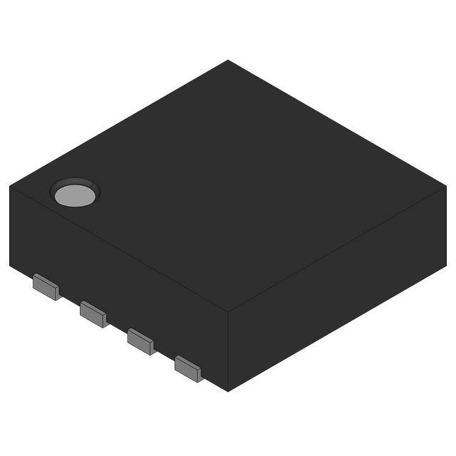


 工商网监
湘ICP备2023018690号
工商网监
湘ICP备2023018690号
