Product
Folder
Order
Now
Support &
Community
Tools &
Software
Technical
Documents
TLA2021, TLA2022, TLA2024
SBAS846 – NOVEMBER 2017
TLA202x Cost-Optimized, Ultra-Small, 12-Bit, System-Monitoring ADCs
1 Features
3 Description
•
•
•
The TLA2021, TLA2022, and TLA2024 devices
(TLA202x) are easy-to-use, low-power, 12-bit deltasigma (ΔΣ) analog-to-digital converters (ADCs)
targeted for any type of system-monitoring
applications (such as supply or battery voltage
supervision, current sensing, or temperature
measurements). Offered in an ultra-small, leadless,
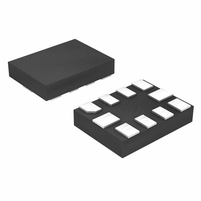
10-pin X2QFN package, the TLA2021 and TLA2022
are single-channel ADCs while the TLA2024 features
a flexible input multiplexer (MUX) with two differential
or four single-ended input measurement options.
1
•
•
•
•
•
Industry’s Lowest-Cost 12-Bit Delta-Sigma ADCs
Ultra-Small X2QFN Package: 2 mm × 1.5 mm
Highly Integrated:
– 4 Single-Ended or 2 Differential Inputs Make
the TLA2024 the Industry’s Highest Channel
Density ADC (0.75 mm² per Channel)
– PGA (TLA2022 and TLA2024 Only)
– Voltage Reference
– Oscillator
Low Current Consumption: 150 µA
Wide Supply Range: 2 V to 5.5 V
Programmable Data Rate: 128 SPS to 3.3 kSPS
I2C™ Compatible Interface:
– Supports Standard-Mode and Fast-Mode
– Three Pin-Selectable I2C Addresses
Operating Temperature Range: –40°C to +85°C
The TLA202x integrate a voltage reference and
oscillator. Additionally, the TLA2022 and TLA2024
include a programmable gain amplifier (PGA) with
selectable input ranges from ±256 mV to ±6.144 V,
enabling both large- and small-signal measurements.
The TLA202x communicate via an I2C-compatible
interface and operate in either continuous or singleshot conversion mode. The devices automatically
power down after one conversion in single-shot
conversion mode, significantly reducing power
consumption during idle periods.
2 Applications
•
•
•
•
•
•
Personal Electronics:
– TVs, Tablets, Cell Phones
– Wearables
– Drones, Toys
Home and Kitchen Appliances
Building Automation:
– HVACs, Smoke Detectors
Battery Voltage and Current Monitoring
Temperature Sensing
Battery-Powered, Portable Instrumentation
All of these features, along with a wide operating
supply voltage range, make the TLA202x suitable for
power- and space-constrained, system-monitoring
applications.
Device Information(1)
PART NUMBER
PACKAGE
BODY SIZE (NOM)
TLA2021
TLA2022
X2QFN (10)
1.50 mm × 2.00 mm
TLA2024
(1) For all available packages, see the orderable addendum at
the end of the data sheet.
System-Monitoring Application Example
3.3 V
3.3 V
Power Supply
Monitoring
3.3 V
RSHUNT
VDD
Current
Sense
Amplifier
Voltage
Reference
AIN0
SCL
AIN1
Analog Output
Temperature
Sensor IC
3.3 V
AIN2
Mux
12-Bit
û¯
ADC
PGA
I2C
Interface
SDA
I2C Bus
ADDR
AIN3
Oscillator
TLA2024
RBIAS
GND
Thermistor
Copyright © 2017, Texas Instruments Incorporated
1
An IMPORTANT NOTICE at the end of this data sheet addresses availability, warranty, changes, use in safety-critical applications,
intellectual property matters and other important disclaimers. PRODUCTION DATA.
�TLA2021, TLA2022, TLA2024
SBAS846 – NOVEMBER 2017
www.ti.com
Table of Contents
1
2
3
4
5
6
7
8
Features ..................................................................
Applications ...........................................................
Description .............................................................
Revision History.....................................................
Device Comparison Table.....................................
Pin Configuration and Functions .........................
Specifications.........................................................
1
1
1
2
3
3
4
7.1
7.2
7.3
7.4
7.5
7.6
7.7
4
4
4
4
5
6
7
Absolute Maximum Ratings ......................................
ESD Ratings..............................................................
Recommended Operating Conditions.......................
Thermal Information ..................................................
Electrical Characteristics...........................................
I2C Timing Requirements..........................................
Typical Characteristics ..............................................
8.6 Register Maps ......................................................... 17
9
9.1 Application Information............................................ 19
9.2 Typical Application .................................................. 23
10 Power Supply Recommendations ..................... 24
10.1 Power-Supply Sequencing.................................... 24
10.2 Power-Supply Decoupling..................................... 24
11 Layout................................................................... 25
11.1 Layout Guidelines ................................................. 25
11.2 Layout Example .................................................... 26
12 Device and Documentation Support ................. 27
12.1
12.2
12.3
12.4
12.5
12.6
12.7
Detailed Description .............................................. 8
8.1
8.2
8.3
8.4
8.5
Application and Implementation ........................ 19
Overview ................................................................... 8
Functional Block Diagrams ....................................... 8
Feature Description................................................... 9
Device Functional Modes........................................ 12
Programming........................................................... 13
Device Support......................................................
Related Links ........................................................
Receiving Notification of Documentation Updates
Community Resources..........................................
Trademarks ...........................................................
Electrostatic Discharge Caution ............................
Glossary ................................................................
27
27
27
27
27
27
27
13 Mechanical, Packaging, and Orderable
Information ........................................................... 28
4 Revision History
NOTE: Page numbers for previous revisions may differ from page numbers in the current version.
2
DATE
REVISION
NOTES
November 2017
*
Initial release.
Submit Documentation Feedback
Copyright © 2017, Texas Instruments Incorporated
Product Folder Links: TLA2021 TLA2022 TLA2024
�TLA2021, TLA2022, TLA2024
www.ti.com
SBAS846 – NOVEMBER 2017
5 Device Comparison Table
DEVICE
RESOLUTION
(Bits)
MAXIMUM SAMPLE
RATE
(SPS)
INPUT CHANNELS,
DIFFERENTIAL
(Single-Ended)
PGA
INTERFACE
TLA2021
12
3300
1 (1)
No
I2C
TLA2022
12
3300
1 (1)
Yes
I2C
TLA2024
12
3300
2 (4)
Yes
I2C
6 Pin Configuration and Functions
TLA2021 and TLA2022 RUG Package
10-Pin X2QFN
Top View
1
9
SDA
ADDR
1
NC
2
8
VDD
NC
GND
3
7
NC
AIN0
4
6
NC
9
SDA
2
8
VDD
GND
3
7
AIN3
AIN0
4
6
AIN2
5
5
10
10
ADDR
SCL
SCL
TLA2024 RUG Package
10-Pin X2QFN
Top View
Not to scale
AIN1
AIN1
Not to scale
Pin Functions
PIN
TYPE
DESCRIPTION
NAME
TLA2021,
TLA2022
TLA2024
ADDR
1
1
Digital input
I2C slave address select pin. See the I2C Address Selection section for details.
AIN0
4
4
Analog input
Analog input 0 (1)
AIN1
5
5
Analog input
Analog input 1 (1)
AIN2
—
6
Analog input
Analog input 2 (1)
AIN3
—
7
Analog input
Analog input 3 (1)
GND
3
3
Supply
NC
2, 6, 7
2
—
SCL
10
10
Digital input
SDA
9
9
Digital I/O
VDD
8
8
Supply
(1)
Ground
No connect; always leave floating
Serial clock input. Connect to VDD using a pullup resistor.
Serial data input and output. Connect to VDD using a pullup resistor.
Power supply. Connect a 0.1-µF, power-supply decoupling capacitor to GND.
Float unused analog inputs, or tie unused analog inputs to GND.
Submit Documentation Feedback
Copyright © 2017, Texas Instruments Incorporated
Product Folder Links: TLA2021 TLA2022 TLA2024
3
�TLA2021, TLA2022, TLA2024
SBAS846 – NOVEMBER 2017
www.ti.com
7 Specifications
7.1 Absolute Maximum Ratings (1)
MIN
MAX
UNIT
Power-supply voltage
VDD to GND
–0.3
7
Analog input voltage
AIN0, AIN1, AIN2, AIN3
GND – 0.3
VDD + 0.3
Digital input voltage
SDA, SCL, ADDR
GND – 0.3
7
Input current
Continuous, any pin except power-supply pins
–10
10
Junction, TJ
–40
125
Storage, Tstg
–60
125
Temperature
(1)
V
mA
°C
Stresses beyond those listed under Absolute Maximum Ratings may cause permanent damage to the device. These are stress ratings
only, which do not imply functional operation of the device at these or any other conditions beyond those indicated under Recommended
Operating Conditions. Exposure to absolute-maximum-rated conditions for extended periods may affect device reliability.
7.2 ESD Ratings
VALUE
V(ESD)
(1)
(2)
Electrostatic discharge
Human-body model (HBM), per ANSI/ESDA/JEDEC JS-001 (1)
±2000
Charged-device model (CDM), per JEDEC specification JESD22-C101 (2)
±500
UNIT
V
JEDEC document JEP155 states that 500-V HBM allows safe manufacturing with a standard ESD control process.
JEDEC document JEP157 states that 250-V CDM allows safe manufacturing with a standard ESD control process.
7.3 Recommended Operating Conditions
over operating ambient temperature range (unless otherwise noted)
MIN
NOM
MAX
UNIT
POWER SUPPLY
VDD to GND
2
5.5
V
±0.256
±6.144
V
GND
VDD
V
GND
5.5
V
–40
85
°C
ANALOG INPUTS (1)
FSR
Full-scale input voltage range (2)
(VIN = VAINP – VAINN)
V(AINx)
Absolute input voltage
DIGITAL INPUTS
Digital input voltage
TEMPERATURE
TA
(1)
(2)
Operating ambient temperature
AINP and AINN denote the selected positive and negative inputs. On the TLA2024, AINx denotes one of the four available analog inputs.
This parameter expresses the full-scale range of the ADC scaling. No more than VDD + 0.3 V or 5.5 V (whichever is smaller) must be
applied to this device. See the Full-Scale Range (FSR) and LSB Size section more information.
7.4 Thermal Information
TLA202x
THERMAL METRIC (1)
RUG (X2QFN)
UNIT
10 PINS
RθJA
Junction-to-ambient thermal resistance
245.2
°C/W
RθJC(top)
Junction-to-case (top) thermal resistance
69.3
°C/W
RθJB
Junction-to-board thermal resistance
172.0
°C/W
ψJT
Junction-to-top characterization parameter
8.2
°C/W
ψJB
Junction-to-board characterization parameter
170.8
°C/W
RθJC(bot)
Junction-to-case (bottom) thermal resistance
N/A
°C/W
(1)
4
For more information about traditional and new thermal metrics, see the Semiconductor and IC Package Thermal Metrics application
report.
Submit Documentation Feedback
Copyright © 2017, Texas Instruments Incorporated
Product Folder Links: TLA2021 TLA2022 TLA2024
�TLA2021, TLA2022, TLA2024
www.ti.com
SBAS846 – NOVEMBER 2017
7.5 Electrical Characteristics
minimum and maximum specifications apply from TA = –40°C to +85°C; typical specifications are at TA = 25°C; all
specifications are at VDD = 3.3 V, data rate = 128 SPS, and FSR = ±2.048 V (unless otherwise noted)
PARAMETER
TEST CONDITIONS
MIN
TYP
MAX
UNIT
ANALOG INPUT
FSR = ±6.144 V (1)
Common-mode input impedance
10
FSR = ±4.096 V (1), FSR = ±2.048 V
6
FSR = ±1.024 V
3
FSR = ±0.512 V, FSR = ±0.256 V
FSR = ±6.144 V
Differential input impedance
MΩ
100
(1)
22
FSR = ±4.096 V (1)
15
FSR = ±2.048 V
4.9
FSR = ±1.024 V
2.4
FSR = ±0.512 V, ±0.256 V
710
MΩ
kΩ
SYSTEM PERFORMANCE
Resolution (no missing codes)
DR
12
Data rate
Data rate variation
All data rates
–10%
Integral nonlinearity (2)
INL
LSB
±1
Offset drift
LSB
0.01
Gain error (3)
SPS
10%
1
Offset error
Gain drift
Bits
128, 250, 490, 920, 1600, 2400, 3300
LSB/°C
0.05%
(3)
10
ppm/°C
PSRR
Power-supply rejection ratio
85
dB
CMRR
Common-mode rejection ratio
90
dB
DIGITAL INPUT/OUTPUT
VIL
Logic input level, low
VIH
Logic input level, high
VOL
Logic output level, low
IOL = 3 mA
Input leakage current
GND < VDigital Input < VDD
GND
0.3 VDD
V
0.7 VDD
5.5
V
0.4
V
10
µA
GND
0.15
–10
POWER SUPPLY
IVDD
Supply current
PD
Power dissipation
(1)
(2)
(3)
Power-down
0.5
Operating
150
VDD = 5 V
0.9
VDD = 3.3 V
0.5
VDD = 2 V
0.3
µA
mW
This parameter expresses the full-scale range of the ADC scaling. No more than VDD + 0.3 V or 5.5 V (whichever is smaller) must be
applied to this device. See the Full-Scale Range (FSR) and LSB Size section for more information.
Best-fit INL; covers 99% of full-scale.
Includes all errors from onboard PGA and voltage reference.
Submit Documentation Feedback
Copyright © 2017, Texas Instruments Incorporated
Product Folder Links: TLA2021 TLA2022 TLA2024
5
�TLA2021, TLA2022, TLA2024
SBAS846 – NOVEMBER 2017
www.ti.com
7.6 I2C Timing Requirements
over operating ambient temperature range and VDD = 2 V to 5.5 V (unless otherwise noted)
MIN
MAX
UNIT
100
kHz
STANDARD-MODE
fSCL
SCL clock frequency
10
tLOW
Pulse duration, SCL low
4.7
µs
tHIGH
Pulse duration, SCL high
4.0
µs
tHD;STA
Hold time, (repeated) START condition.
After this period, the first clock pulse is generated.
4
µs
tSU;STA
Setup time, repeated START condition
4.7
µs
tHD;DAT
Hold time, data
0
µs
tSU;DAT
Setup time, data
tr
Rise time, SCL, SDA
1000
ns
tf
Fall time, SCL, SDA
250
ns
tSU;STO
Setup time, STOP condition
4.0
tBUF
Bus free time, between STOP and START condition
4.7
tVD;DAT
Valid time, data
3.45
µs
tVD;ACK
Valid time, acknowledge
3.45
µs
400
kHz
250
ns
µs
µs
FAST-MODE
fSCL
SCL clock frequency
10
tLOW
Pulse duration, SCL low
1.3
µs
tHIGH
Pulse duration, SCL high
0.6
µs
tHD;STA
Hold time, (repeated) START condition.
After this period, the first clock pulse is generated.
0.6
µs
tSU;STA
Setup time, repeated START condition
0.6
µs
tHD;DAT
Hold time, data
0
µs
tSU;DAT
Setup time, data
tr
Rise time, SCL, SDA
tf
Fall time, SCL, SDA
tSU;STO
Setup time, STOP condition
0.6
tBUF
Bus free time, between STOP and START condition
1.3
tVD;DAT
Valid time, data
0.9
µs
tVD;ACK
Valid time, acknowledge
0.9
µs
100
tf
SDA
ns
20
ns
300
ns
µs
µs
tSU;DAT
tr
70%
30%
...
cont.
tHD;DAT
tf
tVD;DAT
tHIGH
tr
70%
30%
70%
30%
SCL
...
cont.
tLOW
tHD;STA
S
300
9th clock
1 / fSCL
1st clock cycle
tBUF
SDA
tSU;STA
tVD;ACK
tHD;STA
tSU;STO
70%
30%
SCL
Sr
9th clock
P
S
Figure 1. I2C Timing Requirements
6
Submit Documentation Feedback
Copyright © 2017, Texas Instruments Incorporated
Product Folder Links: TLA2021 TLA2022 TLA2024
�TLA2021, TLA2022, TLA2024
www.ti.com
SBAS846 – NOVEMBER 2017
7.7 Typical Characteristics
at FSR = ±2.048 V and DR = 128 SPS (unless otherwise noted)
3
250
Power-Down Current (PA)
Operating Current (PA)
200
150
100
50
0
-40
VDD = 5 V
VDD = 3 V
VDD = 2 V
2.5
VDD = 5 V
VDD = 3 V
VDD = 2 V
-20
0
20
40
Temperature (qC)
60
80
2
1.5
1
0.5
100
0
-40
Figure 2. Operating Current vs Temperature
-20
0
20
40
Temperature (qC)
60
80
100
Figure 3. Power-Down Current vs Temperature
6
VDD = 5 V
VDD = 3 V
VDD = 2 V
Data Rate Error (%)
4
2
0
-2
-4
-6
-40
-20
0
20
40
Temperature (qC)
60
80
100
Figure 4. Data Rate vs Temperature
Submit Documentation Feedback
Copyright © 2017, Texas Instruments Incorporated
Product Folder Links: TLA2021 TLA2022 TLA2024
7
�TLA2021, TLA2022, TLA2024
SBAS846 – NOVEMBER 2017
www.ti.com
8 Detailed Description
8.1 Overview
The TLA202x are a family of very small, low-power, 12-bit, delta-sigma (ΔΣ) analog-to-digital converters (ADCs).
The TLA202x consist of a ΔΣ ADC core with an internal voltage reference, a clock oscillator, and an I2C
interface. The TLA2022 and TLA2024 also integrate a programmable gain amplifier (PGA). Figure 5, Figure 6,
and Figure 7 show the functional block diagrams of the TLA2024, TLA2022, and TLA2021, respectively.
The TLA202x ADC core measures a differential signal, VIN, that is the difference of VAINP and VAINN. The
converter core consists of a differential, switched-capacitor ΔΣ modulator followed by a digital filter. This
architecture results in a very strong attenuation of any common-mode signals. Input signals are compared to the
internal voltage reference. The digital filter receives a high-speed bitstream from the modulator and outputs a
code proportional to the input voltage.
The TLA202x have two available conversion modes: single-shot and continuous-conversion. In single-shot
conversion mode, the ADC performs one conversion of the input signal upon request, stores the conversion
value to an internal conversion register, and then enters a power-down state. This mode is intended to provide
significant power savings in systems that only require periodic conversions or when there are long idle periods
between conversions. In continuous-conversion mode, the ADC automatically begins a conversion of the input
signal as soon as the previous conversion is complete. The rate of continuous conversion is equal to the
programmed data rate. Data can be read at any time and always reflect the most recently completed conversion.
8.2 Functional Block Diagrams
VDD
TLA2024
Voltage
Reference
Mux
AIN0
ADDR
PGA
AIN1
I 2C
Interface
12-Bit
û¯ ADC
SCL
SDA
AIN2
Oscillator
AIN3
GND
Copyright © 2017, Texas Instruments Incorporated
Figure 5. TLA2024 Block Diagram
VDD
VDD
TLA2022
TLA2021
Voltage
Reference
ADDR
AIN0
PGA
AIN1
Voltage
Reference
12-Bit
û¯ ADC
I2C
Interface
SCL
AIN0
SDA
AIN1
ADDR
I 2C
Interface
12-Bit
û¯ ADC
SCL
SDA
Oscillator
Oscillator
GND
GND
Copyright © 2017, Texas Instruments Incorporated
Copyright © 2017, Texas Instruments Incorporated
Figure 6. TLA2022 Block Diagram
8
Figure 7. TLA2021 Block Diagram
Submit Documentation Feedback
Copyright © 2017, Texas Instruments Incorporated
Product Folder Links: TLA2021 TLA2022 TLA2024
�TLA2021, TLA2022, TLA2024
www.ti.com
SBAS846 – NOVEMBER 2017
8.3 Feature Description
8.3.1 Multiplexer
Figure 8 shows that the TLA2024 contains an analog input multiplexer (MUX). Four single-ended or two
differential signals can be measured. Additionally, AIN0 and AIN1 can be measured differentially to AIN3. The
multiplexer is configured by bits MUX[2:0] in the configuration register. When single-ended signals are measured,
the negative input of the ADC is internally connected to GND by a switch within the multiplexer.
TLA2024
VDD
AIN0
VDD
GND
AINP
AIN1
AINN
VDD
GND
AIN2
VDD
GND
AIN3
GND
GND
Copyright © 2017, Texas Instruments Incorporated
Figure 8. Input Multiplexer
The TLA2021 and TLA2022 do not have an input multiplexer and can either measure one differential signal or
one single-ended signal. For single-ended measurements, connect the AIN1 pin to GND externally. In
subsequent sections of this data sheet, AINP refers to AIN0 and AINN refers to AIN1 for the TLA2021 and
TLA2022.
Electrostatic discharge (ESD) diodes connected to VDD and GND protect the TLA202x analog inputs. Keep the
absolute voltage on any input within the range shown in Equation 1 to prevent the ESD diodes from turning on.
GND – 0.3 V < V(AINX) < VDD + 0.3 V
(1)
If the voltages on the analog input pins can potentially violate these conditions, use external Schottky diodes and
series resistors to limit the input current to safe values (see the Absolute Maximum Ratings table).
Submit Documentation Feedback
Copyright © 2017, Texas Instruments Incorporated
Product Folder Links: TLA2021 TLA2022 TLA2024
9
�TLA2021, TLA2022, TLA2024
SBAS846 – NOVEMBER 2017
www.ti.com
Feature Description (continued)
8.3.2 Analog Inputs
The TLA202x use a switched-capacitor input stage where capacitors are continuously charged and then
discharged to measure the voltage between AINP and AINN. The frequency at which the input signal is sampled
is referred to as the sampling frequency or the modulator frequency (fMOD). The TLA202x have a 1-MHz internal
oscillator that is further divided by a factor of 4 to generate fMOD at 250 kHz. The capacitors used in this input
stage are small, and to external circuitry, the average loading appears resistive. Figure 9 shows this structure.
The capacitor values set the resistance and switching rate. Figure 10 shows the timing for the switches in
Figure 9. During the sampling phase, switches S1 are closed. This event charges CA1 to VAINP, CA2 to VAINN, and
CB to (VAINP – VAINN). During the discharge phase, S1 is first opened and then S2 is closed. CA1 and CA2 then
discharge to approximately 0.7 V and CB discharges to 0 V. This charging draws a very small transient current
from the source driving the TLA202x analog inputs. The average value of this current can be used to calculate
the effective impedance (Zeff), where Zeff = VIN / IAVERAGE.
0.7 V
CA1
AINP
S1
S2
CB
Equivalent
Circuit
0.7 V
ZCM
AINP
ZDIFF
S2
S1
AINN
0.7 V
AINN
CA2
ZCM
fMOD = 250 kHz
0.7 V
Figure 9. Simplified Analog Input Circuit
tSAMPLE
ON
S1
OFF
ON
S2
OFF
Figure 10. S1 and S2 Switch Timing
The common-mode input impedance is measured by applying a common-mode signal to the shorted AINP and
AINN inputs and measuring the average current consumed by each pin. The common-mode input impedance
changes depending on the full-scale range, but is approximately 6 MΩ for the default full-scale range. In
Figure 9, the common-mode input impedance is ZCM.
The differential input impedance is measured by applying a differential signal to the AINP and AINN inputs where
one input is held at 0.7 V. The current that flows through the pin connected to 0.7 V is the differential current and
scales with the full-scale range. In Figure 9, the differential input impedance is ZDIFF.
Consider the typical value of the input impedance. Unless the input source has a low impedance, the TLA202x
input impedance may affect the measurement accuracy. For sources with high-output impedance, buffering may
be necessary. Active buffers introduce noise, offset, and gain errors. Consider all of these factors in highaccuracy applications.
The clock oscillator frequency drifts slightly with temperature; therefore, the input impedances also drift. For most
applications, this input impedance drift is negligible and can be ignored.
10
Submit Documentation Feedback
Copyright © 2017, Texas Instruments Incorporated
Product Folder Links: TLA2021 TLA2022 TLA2024
�TLA2021, TLA2022, TLA2024
www.ti.com
SBAS846 – NOVEMBER 2017
Feature Description (continued)
8.3.3 Full-Scale Range (FSR) and LSB Size
A programmable gain amplifier (PGA) is implemented before the ΔΣ ADC of the TLA2022 and TLA2024. The fullscale range is configured by bits PGA[2:0] in the configuration register and can be set to ±6.144 V, ±4.096 V,
±2.048 V, ±1.024 V, ±0.512 V, or ±0.256 V. Table 1 shows the FSR together with the corresponding LSB size.
Equation 2 shows how to calculate the LSB size from the selected full-scale range.
LSB = FSR / 212
(2)
Table 1. Full-Scale Range and Corresponding LSB Size
(1)
FSR
LSB SIZE
±6.144 V (1)
3 mV
±4.096 V (1)
2 mV
±2.048 V
1 mV
±1.024 V
0.5 mV
±0.512 V
0.25 mV
±0.256 V
0.125 mV
This parameter expresses the full-scale range of the ADC scaling. Do not apply more than VDD + 0.3 V to this device.
The FSR of the TLA2021 is fixed at ±2.048 V.
Analog input voltages must never exceed the analog input voltage limits given in the Absolute Maximum Ratings
table. If a VDD supply voltage greater than 4 V is used, the ±6.144-V full-scale range allows input voltages to
extend up to the supply. Although in this case (or whenever the supply voltage is less than the full-scale range) a
full-scale ADC output code cannot be obtained. For example, with VDD = 3.3 V and FSR = ±4.096 V, only
signals up to VIN = ±3.3 V can be measured. The code range that represents voltages |VIN| > 3.3 V is not used in
this case.
8.3.4 Voltage Reference
The TLA202x have an integrated voltage reference. An external reference cannot be used with these devices.
Errors associated with the initial voltage reference accuracy and the reference drift with temperature are included
in the gain error and gain drift specifications in the Electrical Characteristics table.
8.3.5 Oscillator
The TLA202x have an integrated oscillator running at 1 MHz. No external clock can be applied to operate these
devices. The internal oscillator drifts over temperature and time. The output data rate scales proportionally with
the oscillator frequency.
8.3.6 Output Data Rate and Conversion Time
The TLA202x offer programmable output data rates. Use the DR[2:0] bits in the configuration register to select
output data rates of 128 SPS, 250 SPS, 490 SPS, 920 SPS, 1600 SPS, 2400 SPS, or 3300 SPS.
Conversions in the TLA202x settle within a single cycle, which means the conversion time equals 1 / DR.
Submit Documentation Feedback
Copyright © 2017, Texas Instruments Incorporated
Product Folder Links: TLA2021 TLA2022 TLA2024
11
�TLA2021, TLA2022, TLA2024
SBAS846 – NOVEMBER 2017
www.ti.com
8.4 Device Functional Modes
8.4.1 Reset and Power-Up
The TLA202x reset on power-up and set all bits in the configuration register to the respective default settings.
The TLA202x enter a power-down state after completion of the reset process. The device interface and digital
blocks are active, but no data conversions are performed. The initial power-down state of the TLA202x relieves
systems with tight power-supply requirements from encountering a surge during power-up.
The TLA202x respond to the I2C general-call reset command. When the TLA202x receive a general-call reset
command (06h), an internal reset is performed as if the device is powered up.
8.4.2 Operating Modes
The TLA202x operate in one of two modes: continuous-conversion or single-shot. The MODE bit in the
configuration register selects the respective operating mode.
8.4.2.1 Single-Shot Conversion Mode
When the MODE bit in the configuration register is set to 1, the TLA202x enter a power-down state, and operate
in single-shot conversion mode. This power-down state is the default state for the TLA202x when power is first
applied. Although powered down, the devices respond to commands. The TLA202x remain in this power-down
state until a 1 is written to the operational status (OS) bit in the configuration register. When the OS bit is
asserted, the device powers up in approximately 25 µs, resets the OS bit to 0, and starts a single conversion.
When conversion data are ready for retrieval, the OS bit is set to 1 and the device powers down again. Writing a
1 to the OS bit while a conversion is ongoing has no effect. To switch to continuous-conversion mode, write a 0
to the MODE bit in the configuration register.
8.4.2.2 Continuous-Conversion Mode
In continuous-conversion mode (MODE bit set to 0), the TLA202x perform conversions continuously. When a
conversion is complete, the TLA202x place the result in the conversion data register and immediately begin
another conversion. When writing new configuration settings, the currently ongoing conversion completes with
the previous configuration settings. Thereafter, continuous conversions with the new configuration settings start.
To switch to single-shot conversion mode, write a 1 to the MODE bit in the configuration register or reset the
device.
12
Submit Documentation Feedback
Copyright © 2017, Texas Instruments Incorporated
Product Folder Links: TLA2021 TLA2022 TLA2024
�TLA2021, TLA2022, TLA2024
www.ti.com
SBAS846 – NOVEMBER 2017
8.5 Programming
8.5.1 I2C Interface
The TLA202x use an I2C-compatible (inter-integrated circuit) interface for serial communication. I2C is a 2-wire,
open-drain communication interface that allows communication of a master device with multiple slave devices on
the same bus through the use of device addressing. Each slave device on an I2C bus must have a unique
address. Communication on the I2C bus always takes place between two devices: one acting as the master and
the other as the slave. Both the master and slave can receive and transmit data, but the slave can only read or
write under the direction of the master. The TLA202x always act as I2C slave devices.
An I2C bus consists of two lines: SDA and SCL. SDA carries data and SCL provides the clock. Devices on the
I2C bus drive the bus lines low by connecting the lines to ground; the devices never drive the bus lines high.
Instead, the bus wires are pulled high by pullup resistors; thus, the bus wires are always high when a device is
not driving the lines low. As a result of this configuration, two devices do not conflict. If two devices drive the bus
simultaneously, there is no driver contention.
See the I2C-Bus Specification and User Manual from NXP Semiconductors™ for more details.
8.5.1.1 I2C Address Selection
The TLA202x have one address pin (ADDR) that configures the I2C address of the device. The ADDR pin can
connect to GND, VDD, or SCL (as shown in Table 2), which allows three different addresses to be selected with
one pin. At the start of every transaction, that is between the START condition (first falling edge of SDA) and the
first falling SCL edge of the address byte, the TLA202x decode its address configuration again.
Table 2. ADDR Pin Connection and Corresponding Slave Address
ADDR PIN CONNECTION
SLAVE ADDRESS
GND
1001 000
VDD
1001 001
SCL
1001 011
8.5.1.2 I2C Interface Speed
The TLA202x support I2C interface speeds up to 400 kbit/s. Standard-mode (Sm) with bit rates up to 100 kbit/s,
and fast-mode (Fm) with bit rates up to 400 kbit/s are supported. Fast-mode plus (Fm+) and high-speed mode
(Hs-mode) are not supported.
8.5.1.3 Serial Clock (SCL) and Serial Data (SDA)
The serial clock (SCL) line is used to clock data in and out of the device. The master always drives the clock line.
The TLA202x cannot act as a master and as a result can never drive SCL.
The serial data (SDA) line allows for bidirectional communication between the host (the master) and the TLA202x
(the slave). When the master reads from a TLA202x, the TLA202x drives the data line; when the master writes to
a TLA202x, the master drives the data line.
Data on the SDA line must be stable during the high period of the clock. The high or low state of the data line
can only change when the SCL line is low. One clock pulse is generated for each data bit transferred. When in
an idle state, the master should hold SCL high.
Submit Documentation Feedback
Copyright © 2017, Texas Instruments Incorporated
Product Folder Links: TLA2021 TLA2022 TLA2024
13
�TLA2021, TLA2022, TLA2024
SBAS846 – NOVEMBER 2017
www.ti.com
8.5.1.4 I2C Data Transfer Protocol
Figure 11 shows the format of the data transfer. The master initiates all transactions with the TLA202x by
generating a START (S) condition. A high-to-low transition on the SDA line while SCL is high defines a START
condition. The bus is considered to be busy after the START condition.
Following the START condition, the master sends the 7-bit slave address corresponding to the address of the
TLA202x that the master wants to communicate with. The master then sends an eighth bit that is a data direction
bit (R/W). An R/W bit of 0 indicates a write operation, and an R/W bit of 1 indicates a read operation. After the
R/W bit, the master generates a ninth SCLK pulse and releases the SDA line to allow the TLA202x to
acknowledge (ACK) the reception of the slave address by pulling SDA low. In case the device does not
recognize the slave address, the TLA202x holds SDA high to indicate a not acknowledge (NACK) signal.
Next follows the data transmission. If the transaction is a read (R/W = 1), the TLA202x outputs data on SDA. If
the transaction is a write (R/W = 0), the host outputs data on SDA. Data are transferred byte-wise, most
significant bit (MSB) first. The number of bytes that can be transmitted per transfer is unrestricted. Each byte
must be acknowledged (via the ACK bit) by the receiver. If the transaction is a read, the master issues the ACK.
If the transaction is a write, the TLA202x issues the ACK.
The master terminates all transactions by generating a STOP (P) condition. A low-to-high transition on the SDA
line while SCL is high defines a STOP condition. The bus is considered free again tBUF (bus-free time) after the
STOP condition.
SDA
A6 ± A0
D7 ± D0
D7 ± D0
SCL
1-7
8
9
1-8
9
1-8
9
ADDRESS
R/W
ACK
from slave
DATA
ACK
from receiver
DATA
ACK
from receiver
S
START
Condition
P
STOP
Condition
Figure 11. I2C Data Transfer Format
8.5.1.5 Timeout
The TLA202x offer a I2C timeout feature that can be used to recover communication when a serial interface
transmission is interrupted. If the host initiates contact with the TLA202x but subsequently remains idle for 25 ms
before completing a command, the TLA202x interface is reset. If the TLA202x interface resets because of a
timeout condition, the host must abort the transaction and restart the communication again by issuing a new
START condition.
8.5.1.6 I2C General-Call (Software Reset)
The TLA202x respond to the I2C general-call address (0000 000) if the R/W bit is 0. The devices acknowledge
the general-call address and, if the next byte is 06h, the TLA202x reset the internal registers and enter a powerdown state.
14
Submit Documentation Feedback
Copyright © 2017, Texas Instruments Incorporated
Product Folder Links: TLA2021 TLA2022 TLA2024
�TLA2021, TLA2022, TLA2024
www.ti.com
SBAS846 – NOVEMBER 2017
8.5.2 Reading and Writing Register Data
The host can read the conversion data register from the TLA202x, or read and write the configuration register
from and to the TLA202x, respectively. The value of the register pointer (RP), which is the first data byte after the
slave address of a write transaction (R/W = 0), determines the register that is addressed. Table 3 shows the
mapping between the register pointer value and the register that is addressed.
Register data are sent with the most significant byte first, followed by the least significant byte. Within each byte,
data are transmitted most significant bit first.
Table 3. Register Pointer (RP)
REGISTER POINTER
(Hex)
REGISTER
00h
Conversion data register
01h
Configuration register
8.5.2.1 Reading Conversion Data or the Configuration Register
Read the conversion data register or configuration register as shown in Figure 12 by using two I2C
communication frames. The first frame is an I2C write operation where the R/W bit at the end of the slave
address is 0 to indicate a write. In this frame, the host sends the register pointer that points to the register to read
from. The second frame is an I2C read operation where the R/W bit at the end of the slave address is 1 to
indicate a read. The TLA202x transmits the contents of the register in this second I2C frame. The master can
terminate the transmission after any byte by not acknowledging or issuing a START or STOP condition.
When repeatedly reading the same register, the register pointer does not need to be written every time again
because the TLA202x store the value of the register pointer until a write operation modifies the value.
S
SLAVE ADDRESS
W
A
REGISTER POINTER
A
S
SLAVE ADDRESS
R
A
REGISTER DATA (MSB)
A
P
(1)
REGISTER DATA (LSB)
A
P
(1) The master can terminate the transmission after the first byte by not acknowledging.
Figure 12. Reading Register Data
8.5.2.2 Writing the Configuration Register
Write the configuration register as shown in Figure 13 using a single I2C communication frame. The R/W bit at
the end of the salve address is 0 to indicate a write. The host first sends the register pointer that points to the
configuration register, followed by two bytes that represent the register content to write. The TLA202x
acknowledge each received byte.
S
‡‡‡
SLAVE ADDRESS
W
REGISTER DATA (MSB)
A
A
REGISTER POINTER
REGISTER DATA (LSB)
A
A
‡‡‡
P
Figure 13. Writing Register Data
Figure 14 provides a legend for Figure 12 and Figure 13.
From master to slave
S = START condition
P = STOP condition
A = acknowledge (SDA low)
From slave to master
A = not acknowledge (SDA high)
Figure 14. Legend for the I2C Sequence Diagrams
Submit Documentation Feedback
Copyright © 2017, Texas Instruments Incorporated
Product Folder Links: TLA2021 TLA2022 TLA2024
15
�TLA2021, TLA2022, TLA2024
SBAS846 – NOVEMBER 2017
www.ti.com
8.5.3 Data Format
The TLA202x provide 12 bits of data in binary two's-complement format that is left-justified within the 16-bit data
word. A positive full-scale (+FS) input produces an output code of 7FF0h and a negative full-scale (–FS) input
produces an output code of 8000h. The output clips at these codes for signals that exceed full-scale. Table 4
summarizes the ideal output codes for different input signals. Figure 15 shows code transitions versus input
voltage.
Table 4. Input Signal Versus Ideal Output Code
INPUT SIGNAL
VIN = (VAINP – VAINN)
≥ +FS (2
11
IDEAL OUTPUT CODE (1)
11
– 1) / 2
7FF0h
+FS / 211
(1)
0010h
0
0000h
–FS / 211
FFF0h
≤ –FS
8000h
Excludes the effects of noise, INL, offset, and gain errors.
7FF0h
0010h
0000h
FFF0h
...
Output Code
...
7FE0h
8010h
8000h
...
-FS
2
11
-FS
2
0
...
+FS
Input Voltage VIN
2
-1
11
11
+FS
2
-1
11
Figure 15. Code Transition Diagram
NOTE
Single-ended signal measurements, where VAINN = 0 V and VAINP = 0 V to +FS, only use
the positive code range from 0000h to 7FF0h. However, because of device offset, the
TLA202x can still output negative codes in case VAINP is close to 0 V.
16
Submit Documentation Feedback
Copyright © 2017, Texas Instruments Incorporated
Product Folder Links: TLA2021 TLA2022 TLA2024
�TLA2021, TLA2022, TLA2024
www.ti.com
SBAS846 – NOVEMBER 2017
8.6 Register Maps
The TLA202x have two registers that are accessible through the I2C interface using the register pointer (RP). The
conversion data register contains the result of the last conversion and the configuration register changes the
TLA202x operating modes and queries the status of the device. Table 5 lists the access codes for the TLA202x.
Table 5. TLA202x Access Type Codes
Access Type
Code
Description
R
R
Read
R-W
R/W
Read or write
W
W
Write
-n
Value after reset or the default value
8.6.1 Conversion Data Register (RP = 00h) [reset = 0000h]
The 16-bit conversion data register contains the result of the last conversion in binary two's-complement format.
Following power-up, the conversion data register clears to 0, and remains at 0 until the first conversion is
complete.
Figure 16. Conversion Data Register
15
D11
R-0h
7
D3
R-0h
14
D10
R-0h
6
D2
R-0h
13
D9
R-0h
5
D1
R-0h
12
D8
R-0h
4
D0
R-0h
11
D7
R-0h
3
10
D6
R-0h
2
9
D5
R-0h
1
8
D4
R-0h
0
RESERVED
R-0h
Table 6. Conversion Data Register Field Descriptions
Field
Type
Reset
Description
15:4
Bit
D[11:0]
R
000h
12-bit conversion result
3:0
Reserved
R
0h
Always reads back 0h
8.6.2 Configuration Register (RP = 01h) [reset = 8583h]
The 16-bit configuration register controls the operating mode, input selection, data rate, and full-scale range.
Figure 17. Configuration Register
15
OS
R/W-1h
7
14
6
DR[2:0]
R/W-4h
13
MUX[2:0]
R/W-0h
5
12
11
4
3
10
PGA[2:0]
R/W-2h
2
RESERVED
R/W-03h
9
1
8
MODE
R/W-1h
0
Submit Documentation Feedback
Copyright © 2017, Texas Instruments Incorporated
Product Folder Links: TLA2021 TLA2022 TLA2024
17
�TLA2021, TLA2022, TLA2024
SBAS846 – NOVEMBER 2017
www.ti.com
Table 7. Configuration Register Field Descriptions
Bit
Field
Type
Reset
Description
15
OS
R/W
1h
Operational Status or Single-Shot Conversion Start
This bit determines the operational status of the device. OS can only be written
when in a power-down state and has no effect when a conversion is ongoing.
When writing:
0 : No effect
1 : Start a single conversion (when in a power-down state)
When reading:
0 : The device is currently performing a conversion
1 : The device is not currently performing a conversion (default)
14:12
MUX[2:0]
R/W
0h
Input Multiplexer Configuration (TLA2024 only)
These bits configure the input multiplexer.
These bits serve no function on the TLA2021 and TLA2022 and are always set to
000.
000 : AINP = AIN0 and AINN = AIN1 (default)
001 : AINP = AIN0 and AINN = AIN3
010 : AINP = AIN1 and AINN = AIN3
011 : AINP = AIN2 and AINN = AIN3
100 : AINP = AIN0 and AINN = GND
101 : AINP = AIN1 and AINN = GND
110 : AINP = AIN2 and AINN = GND
111 : AINP = AIN3 and AINN = GND
11:9
PGA[2:0]
R/W
2h
Programmable Gain Amplifier Configuration (TLA2022 and TLA2024 Only)
These bits set the FSR of the programmable gain amplifier.
These bits serve no function on the TLA2021 and are always set to 010.
000 : FSR = ±6.144 V (1)
001 : FSR = ±4.096 V (1)
010 : FSR = ±2.048 V (default)
011 : FSR = ±1.024 V
100 : FSR = ±0.512 V
101 : FSR = ±0.256 V
110 : FSR = ±0.256 V
111 : FSR = ±0.256 V
8
MODE
R/W
1h
Operating Mode
This bit controls the operating mode.
0 : Continuous-conversion mode
1 : Single-shot conversion mode or power-down state (default)
7:5
DR[2:0]
R/W
4h
Data Rate
These bits control the data rate setting.
000 : DR = 128 SPS
001 : DR = 250 SPS
010 : DR = 490 SPS
011 : DR = 920 SPS
100 : DR = 1600 SPS (default)
101 : DR = 2400 SPS
110 : DR = 3300 SPS
111 : DR = 3300 SPS
4:0
(1)
18
Reserved
R/W
03h
Always write 03h
This parameter expresses the full-scale range of the ADC scaling. Do not apply more than VDD + 0.3 V to this device.
Submit Documentation Feedback
Copyright © 2017, Texas Instruments Incorporated
Product Folder Links: TLA2021 TLA2022 TLA2024
�TLA2021, TLA2022, TLA2024
www.ti.com
SBAS846 – NOVEMBER 2017
9 Application and Implementation
NOTE
Information in the following applications sections is not part of the TI component
specification, and TI does not warrant its accuracy or completeness. TI’s customers are
responsible for determining suitability of components for their purposes. Customers should
validate and test their design implementation to confirm system functionality.
9.1 Application Information
The following sections give example circuits and suggestions for using the TLA202x in various applications.
9.1.1 Basic Interface Connections
Figure 18 shows the principle I2C connections for the TLA202x.
VDD
1-k to 10-k
Pullup Resistors
10
Device
1
SCL
ADDR
SCL
SDA
SDA
9
VDD
2
NC
VDD
8
3
GND
AIN3
7
4
AIN0
AIN2
6
Microcontroller or
Microprocessor
With I2C Port
0.1 F
AIN1
5
Copyright © 2017, Texas Instruments Incorporated
Figure 18. Typical Interface Connections of the TLA202x
The TLA202x interface directly to standard-mode or fast-mode I2C controllers. Any microcontroller I2C peripheral,
including master-only and single-master I2C peripherals, operates with the TLA202x. The TLA202x do not
perform clock-stretching (that is, the devices never pull the clock line low), so this function does not need to be
provided for unless other clock-stretching devices are present on the same I2C bus.
Pullup resistors are required on both the SDA and SCL lines because I2C bus drivers are open-drain. The size of
these resistors depends on the bus operating speed and capacitance of the bus lines. Higher-value resistors
yield lower power consumption when the bus lines are pulled low, but increase the transition times on the bus,
which limits the bus speed. Lower-value resistors allow higher interface speeds, but at the expense of higher
power consumption when the bus lines are pulled low. Long bus lines have higher capacitance and require
smaller pullup resistors to compensate. Do not use resistors that are too small because the bus drivers may be
unable to pull the bus lines low.
See the I2C-Bus Specification and User Manual from NXP Semiconductors for more details on pullup resistor
sizing.
Submit Documentation Feedback
Copyright © 2017, Texas Instruments Incorporated
Product Folder Links: TLA2021 TLA2022 TLA2024
19
�TLA2021, TLA2022, TLA2024
SBAS846 – NOVEMBER 2017
www.ti.com
Application Information (continued)
9.1.2 Connecting Multiple Devices
Up to three TLA202x devices can be connected to a single I2C bus by using different address pin configurations
for each device. Use the address pin to set the TLA202x to one of three different I2C addresses. Figure 19
shows an example with three TLA202x devices on the same I2C bus. One set of pullup resistors is required per
bus line. The pullup resistor values may need to decrease to compensate for the additional bus capacitance
presented by multiple devices and increased line length.
10
Device
SCL
1
ADDR
SDA
9
2
NC
VDD
8
3
GND
AIN3
7
4
AIN0
AIN2
6
VDD
AIN1
5
1-k to 10-k
Pullup Resistors
SCL
10
VDD
Device
Microcontroller or
Microprocessor
With I2C Port
SCL
SDA
1
ADDR
SDA
9
2
NC
VDD
8
3
GND
AIN3
7
4
AIN0
AIN2
6
AIN1
5
10
Device
SCL
1
ADDR
SDA
9
2
NC
VDD
8
3
GND
AIN3
7
4
AIN0
AIN2
6
AIN1
5
Copyright © 2017, Texas Instruments Incorporated
NOTE: The TLA202x power and input connections are omitted for clarity. The ADDR pin selects the I2C address.
Figure 19. Connecting Multiple TLA202x Devices
20
Submit Documentation Feedback
Copyright © 2017, Texas Instruments Incorporated
Product Folder Links: TLA2021 TLA2022 TLA2024
�TLA2021, TLA2022, TLA2024
www.ti.com
SBAS846 – NOVEMBER 2017
Application Information (continued)
9.1.3 Single-Ended Signal Measurements
The TLA2021 and TLA2022 can measure one single-ended signal, and the TLA2024 up to four single-ended
signals. To measure single-ended signals with the TLA2021 and TLA2022, connect AIN1 to GND externally. The
TLA2024 measures single-ended signals by properly configuring the MUX[2:0] bits (settings 100 to 111) in the
configuration register. Figure 20 shows a single-ended connection scheme for the TLA2024 highlighted in red (a
differential connection scheme is shown in green). The single-ended signal range is from 0 V up to the positive
supply or +FS (whichever is lower). Negative voltages cannot be applied to these devices because the TLA202x
can only accept positive voltages with respect to ground. Only the code range from 0000h to 7FF0h (or a subset
thereof in case +FS > VDD) is used in this case.
VDD
TLA2024
CCM
RFLT
VDIF
VCM
+
±
Voltage
Reference
AIN0
CDIF
RFLT
+
ADDR
AIN1
12-Bit
û¯ ADC
PGA
AIN2
+
I 2C
Interface
SCL
SDA
CCM
±
RFLT
VSE
Mux
Oscillator
AIN3
CSE
±
GND
Copyright © 2017, Texas Instruments Incorporated
Figure 20. Filter Implementation for Single-Ended and Differential Signal Measurements
The TLA2024 also allows AIN3 to serve as a common point for measurements by appropriately setting the
MUX[2:0] bits. AIN0, AIN1, and AIN2 can all be measured with respect to AIN3. In this configuration, the usable
voltage and code range, respectively, is increased over the single-ended configuration because negative
differential voltages are allowed when GND < V(AIN3) < VDD. Assume the following settings for example: VDD =
5 V, FSR = ±2.048 V, AINP = AIN0, and AINN = AIN3 = 2.5 V. In this case, the voltage at AIN0 can swing from
V(AIN0) = 2.5 V – 2.048 V to 2.5 V + 2.048 V using the entire full-scale range.
9.1.4 Analog Input Filtering
Analog input filtering serves two purposes:
1. Limits the effect of aliasing during the ADC sampling process
2. Attenuates unwanted noise components outside the bandwidth of interest
In most cases, a first-order resistor capacitor (RC) filter is sufficient to completely eliminate aliasing or to reduce
the effect of aliasing to a level within the noise floor of the sensor. A good starting point for a system design with
the TLA202x is to use a differential RC filter with a cutoff frequency set somewhere between the selected output
data rate and 25 kHz. Make the series resistor values as small as possible to reduce voltage drops across the
resistors caused by the device input currents to a minimum. However, the resistors should be large enough to
limit the current into the analog inputs to less than 10 mA in the event of an overvoltage. Then choose the
differential capacitor value to achieve the target filter cutoff frequency. Common-mode filter capacitors to GND
can be added as well, but should always be at least ten times smaller than the differential filter capacitor.
Figure 20 shows an example of filtering a differential signal (AIN0, AIN1), and a single-ended signal (AIN3).
Equation 3 and Equation 4 show how to calculate the filter cutoff frequencies (fCO) in the differential and singleended cases, respectively.
fCO DIF = 1 / (2π · 2 · RFLT · CDIF)
fCO SE = 1 / (2π · RFLT · CSE)
(3)
(4)
Submit Documentation Feedback
Copyright © 2017, Texas Instruments Incorporated
Product Folder Links: TLA2021 TLA2022 TLA2024
21
�TLA2021, TLA2022, TLA2024
SBAS846 – NOVEMBER 2017
www.ti.com
Application Information (continued)
9.1.5 Duty Cycling To Reduce Power Consumption
For applications where power consumption is critical, the TLA202x support duty cycling that yield significant
power savings by periodically requesting high data rate readings at an effectively lower data rate. For example,
an TLA202x in power-down state with a data rate set to 3300 SPS can be operated by a microcontroller that
instructs a single-shot conversion every 7.81 ms (128 SPS). A conversion at 3300 SPS requires approximately
0.3 ms, so the TLA202x enters power-down state for the remaining 7.51 ms. In this configuration, the TLA202x
consume approximately 1/25th the power that is otherwise consumed in continuous-conversion mode. The duty
cycling rate is arbitrary and is defined by the master controller.
9.1.6 I2C Communication Sequence Example
This section provides an example of an I2C communication sequence between a microcontroller (the master) and
a TLA2024 (the slave) configured with a slave address of 1001 000 to start a single-shot conversion and
subsequently read the conversion result.
1. Write the configuration register as shown in Figure 21 to configure the device (for example, write MUX[2:0] =
000, PGA[2:0] = 010, MODE = 1, and DR[2:0] = 110) and start a single-shot conversion (OS = 1):
S
‡‡‡
SLAVE ADDRESS (1001 000)
CONFIGURATION DATA (85h)
W
A
A
REGISTER POINTER (01h)
CONFIGURATION DATA (C0h)
A
A
‡‡‡
P
Figure 21. Write the Configuration Register
2. Wait at least t = 1 / DR ± 10% for the conversion to complete.
Alternatively, poll the OS bit for a 1 as shown in Figure 22 to determine when the conversion result is ready
for retrieval. This option does not work in continuous-conversion mode because the OS bit always reads 0.
S
‡‡‡
SLAVE ADDRESS (1001 000)
R
A
CONFIGURATION DATA (MSB)
A
CONFIGURATION DATA (LSB)
A
P
Figure 22. Read the Configuration Register to Check for OS = 1
3. Then, as shown in Figure 23, read the conversion data register:
S
SLAVE ADDRESS (1001 000)
W
A
REGISTER POINTER (00h)
A
S
SLAVE ADDRESS (1001 000)
R
A
CONVERSION DATA (MSB)
A
P
CONVERSION DATA (LSB)
A
P
Figure 23. Read the Conversion Data Register
4. Start a new single-shot conversion by writing a 1 to the OS bit in the configuration register.
To save time, a new conversion can also be started (step 4) before reading the conversion result (step 3).
Figure 24 lists a legend for Figure 21 to Figure 23.
From master to slave
S = START condition
P = STOP condition
A = acknowledge (SDA low)
From slave to master
A = not acknowledge (SDA high)
Figure 24. Legend for the I2C Sequence Diagrams
22
Submit Documentation Feedback
Copyright © 2017, Texas Instruments Incorporated
Product Folder Links: TLA2021 TLA2022 TLA2024
�TLA2021, TLA2022, TLA2024
www.ti.com
SBAS846 – NOVEMBER 2017
9.2 Typical Application
This application example describes how to use the TLA2024 to monitor two different supply voltage rails in a
system. Figure 25 shows a typical implementation for monitoring two supply voltage rails.
3.3 V
0.1 F
3.3 V
VDD
3.3 V
100
0.47 F
SCL
AIN1
Mux
1.8 V
1-k to 10-k
Pullup Resistors
Voltage
Reference
AIN0
12-Bit
û¯
ADC
PGA
AIN2
2
I2C Bus
SDA
IC
Interface
ADDR
100
Oscillator
AIN3
0.47 F
TLA2024
GND
Copyright © 2017, Texas Instruments Incorporated
Figure 25. Monitoring Two Supply Voltage Rails Using the TLA2024
9.2.1 Design Requirements
Table 8 lists the design requirements for this application.
Table 8. Design Requirements
DESIGN PARAMETER
VALUE
Device supply voltage
3.3 V
Voltage rails to monitor
1.8 V, 3.3 V
Measurement accuracy
±0.5%
Update rate
1 ms per rail
9.2.2 Detailed Design Procedure
The analog inputs, AIN0 and AIN3, connect directly to the supply voltage rails that are monitored through RC
filter resistors. Small filter resistor values of 100 Ω are chosen to reduce voltage drops, and therefore offset
errors, caused by the input currents of the TLA2024 to a minimum. Filter capacitors of 0.47 µF are chosen to set
the filter cutoff frequencies at 3.39 kHz. In order to get one reading from each of the two supplies within 2 ms, a
data rate of 2400 SPS is selected. The device is set up for single-ended measurements using MUX[2:0] settings
100 and 101. A FSR = ±4.096 V is selected to measure the 3.3-V rail. The same FSR can also be used to
measure the 1.8-V rail or the FSR can be set to FSR = ±2.048 V.
Submit Documentation Feedback
Copyright © 2017, Texas Instruments Incorporated
Product Folder Links: TLA2021 TLA2022 TLA2024
23
�TLA2021, TLA2022, TLA2024
SBAS846 – NOVEMBER 2017
www.ti.com
9.2.3 Application Curve
The measurement results in Figure 26 show that the two supplies can be measured with ±0.5% accuracy over
the complete operating ambient temperature range without any offset or gain calibration.
0.1
Measurement Error (%)
0.075
0.05
0.025
0
-0.025
-0.05
-0.075
3.3 V rail monitor
1.8 V rail monitor
-0.1
-40
-20
0
20
40
Temperature (qC)
60
80
100
Figure 26. Measurement Error vs Temperature
10 Power Supply Recommendations
The device requires a single unipolar supply (VDD) to power the analog and digital circuitry of the device.
10.1 Power-Supply Sequencing
Wait approximately 50 µs after VDD is stabilized before communicating with the device to allow the power-up
reset process to complete.
10.2 Power-Supply Decoupling
Good power-supply decoupling is important to achieve optimum performance. As shown in Figure 27, VDD must
be decoupled with at least a 0.1-µF capacitor to GND. The 0.1-µF bypass capacitor supplies the momentary
bursts of extra current required from the supply when the device is converting. Place the bypass capacitor as
close to the power-supply pin of the device as possible using low-impedance connections. Use multilayer
ceramic chip capacitors (MLCCs) that offer low equivalent series resistance (ESR) and inductance (ESL)
characteristics for power-supply decoupling purposes. For very sensitive systems, or for systems in harsh noise
environments, avoid using vias to connect the capacitors to the device pins for better noise immunity. The use of
multiple vias in parallel lowers the overall inductance and is beneficial for connections to ground planes.
10
Device
SCL
VDD
1
ADDR
SDA
9
2
NC
VDD
8
3
GND
AIN3
7
4
AIN0
AIN2
6
0.1 F
AIN1
5
Figure 27. TLA202x Power-Supply Decoupling
24
Submit Documentation Feedback
Copyright © 2017, Texas Instruments Incorporated
Product Folder Links: TLA2021 TLA2022 TLA2024
�TLA2021, TLA2022, TLA2024
www.ti.com
SBAS846 – NOVEMBER 2017
11 Layout
11.1 Layout Guidelines
Employ best design practices when laying out a printed-circuit board (PCB) for both analog and digital
components. For optimal performance, separate the analog components such as ADCs, amplifiers, references,
digital-to-analog converters (DACs), and analog MUXs from digital components such as microcontrollers,
complex programmable logic devices (CPLDs), field-programmable gate arrays (FPGAs), radio frequency (RF)
transceivers, universal serial bus (USB) transceivers, and switching regulators. Figure 28 shows an example of
good component placement. Although Figure 28 provides a good example of component placement, the best
placement for each application is unique to the geometries, components, and PCB fabrication capabilities. That
is, there is no single layout that is perfect for every design and careful consideration must always be used when
designing with any analog component.
Signal
Conditioning
(RC Filters
and
Amplifiers)
Supply
Generation
Microcontroller
Optional: Split
Ground Cut
Device
Ground Fill or
Ground Plane
Ground Fill or
Ground Plane
Optional: Split
Ground Cut
Ground Fill or
Ground Plane
Interface
Transceiver
Connector
or Antenna
Ground Fill or
Ground Plane
Figure 28. System Component Placement
The following points outline some basic recommendations for the layout of the TLA202x to get the best possible
performance of the ADC. A good design can be ruined with a bad circuit layout.
•
•
•
•
•
•
Separate the analog and digital signals. To start, partition the board into analog and digital sections where the
layout permits. Route digital lines away from analog lines to prevent digital noise from coupling back into
analog signals.
Fill void areas on signal layers with ground fill.
Provide good ground return paths. Signal return currents flow on the path of least impedance. If the ground
plane is cut or has other traces that block the current from flowing right next to the signal trace, the ground
plane must find another path to return to the source and complete the circuit. If the ground plane is forced into
a larger path, there is an increased chance of signal radiation. Sensitive signals are more susceptible to EMI
interference.
Use bypass capacitors on supplies to minimize high-frequency noise. Do not place vias between bypass
capacitors and the active device. For best results, place the bypass capacitors on the same layer as close as
possible to the active device.
Consider the resistance and inductance of the routing. Input traces often have resistances that react with the
input bias current and cause an added error voltage. Reduce the loop area enclosed by the source signal and
the return current to minimize the inductance in the path.
For best input combinations with differential measurements, use adjacent analog input lines such as AIN0,
AIN1 and AIN2, AIN3. The differential capacitors must be of high quality. The best ceramic chip capacitors
are C0G (NPO) capacitors, which have stable properties and low-noise characteristics.
Submit Documentation Feedback
Copyright © 2017, Texas Instruments Incorporated
Product Folder Links: TLA2021 TLA2022 TLA2024
25
�TLA2021, TLA2022, TLA2024
SBAS846 – NOVEMBER 2017
www.ti.com
SDA
SCL
ADDR
11.2 Layout Example
VDD
10
1
ADDR
2
NC
3
GND
4
AIN0
SCL
Device
AIN1
SDA
9
VDD
8
AIN3
7
AIN2
6
AIN3
5
AIN1
AIN0
AIN2
Vias connect to either bottom layer or
an internal plane. The bottom layer or
internal plane are dedicated GND planes
Figure 29. TLA2024 X2QFN Package
26
Submit Documentation Feedback
Copyright © 2017, Texas Instruments Incorporated
Product Folder Links: TLA2021 TLA2022 TLA2024
�TLA2021, TLA2022, TLA2024
www.ti.com
SBAS846 – NOVEMBER 2017
12 Device and Documentation Support
12.1 Device Support
12.1.1 Third-Party Products Disclaimer
TI'S PUBLICATION OF INFORMATION REGARDING THIRD-PARTY PRODUCTS OR SERVICES DOES NOT
CONSTITUTE AN ENDORSEMENT REGARDING THE SUITABILITY OF SUCH PRODUCTS OR SERVICES
OR A WARRANTY, REPRESENTATION OR ENDORSEMENT OF SUCH PRODUCTS OR SERVICES, EITHER
ALONE OR IN COMBINATION WITH ANY TI PRODUCT OR SERVICE.
12.2 Related Links
The table below lists quick access links. Categories include technical documents, support and community
resources, tools and software, and quick access to order now.
Table 9. Related Links
PARTS
PRODUCT FOLDER
ORDER NOW
TECHNICAL
DOCUMENTS
TOOLS &
SOFTWARE
SUPPORT &
COMMUNITY
TLA2021
Click here
Click here
Click here
Click here
Click here
TLA2022
Click here
Click here
Click here
Click here
Click here
TLA2024
Click here
Click here
Click here
Click here
Click here
12.3 Receiving Notification of Documentation Updates
To receive notification of documentation updates, navigate to the device product folder on ti.com. In the upper
right corner, click on Alert me to register and receive a weekly digest of any product information that has
changed. For change details, review the revision history included in any revised document.
12.4 Community Resources
The following links connect to TI community resources. Linked contents are provided "AS IS" by the respective
contributors. They do not constitute TI specifications and do not necessarily reflect TI's views; see TI's Terms of
Use.
TI E2E™ Online Community TI's Engineer-to-Engineer (E2E) Community. Created to foster collaboration
among engineers. At e2e.ti.com, you can ask questions, share knowledge, explore ideas and help
solve problems with fellow engineers.
Design Support TI's Design Support Quickly find helpful E2E forums along with design support tools and
contact information for technical support.
12.5 Trademarks
E2E is a trademark of Texas Instruments.
I2C, NXP Semiconductors are trademarks of NXP Semiconductors.
All other trademarks are the property of their respective owners.
12.6 Electrostatic Discharge Caution
This integrated circuit can be damaged by ESD. Texas Instruments recommends that all integrated circuits be handled with
appropriate precautions. Failure to observe proper handling and installation procedures can cause damage.
ESD damage can range from subtle performance degradation to complete device failure. Precision integrated circuits may be more
susceptible to damage because very small parametric changes could cause the device not to meet its published specifications.
12.7 Glossary
SLYZ022 — TI Glossary.
This glossary lists and explains terms, acronyms, and definitions.
Submit Documentation Feedback
Copyright © 2017, Texas Instruments Incorporated
Product Folder Links: TLA2021 TLA2022 TLA2024
27
�TLA2021, TLA2022, TLA2024
SBAS846 – NOVEMBER 2017
www.ti.com
13 Mechanical, Packaging, and Orderable Information
The following pages include mechanical, packaging, and orderable information. This information is the most
current data available for the designated devices. This data is subject to change without notice and revision of
this document. For browser-based versions of this data sheet, refer to the left-hand navigation.
28
Submit Documentation Feedback
Copyright © 2017, Texas Instruments Incorporated
Product Folder Links: TLA2021 TLA2022 TLA2024
�PACKAGE OPTION ADDENDUM
www.ti.com
10-Dec-2020
PACKAGING INFORMATION
Orderable Device
Status
(1)
Package Type Package Pins Package
Drawing
Qty
Eco Plan
(2)
Lead finish/
Ball material
MSL Peak Temp
Op Temp (°C)
Device Marking
(3)
(4/5)
(6)
TLA2021IRUGR
ACTIVE
X2QFN
RUG
10
3000
RoHS & Green
NIPDAU
Level-1-260C-UNLIM
-40 to 85
9AZ
TLA2021IRUGT
ACTIVE
X2QFN
RUG
10
250
RoHS & Green
NIPDAU
Level-1-260C-UNLIM
-40 to 85
9AZ
TLA2022IRUGR
ACTIVE
X2QFN
RUG
10
3000
RoHS & Green
NIPDAU
Level-1-260C-UNLIM
-40 to 85
19J
TLA2022IRUGT
ACTIVE
X2QFN
RUG
10
250
RoHS & Green
NIPDAU
Level-1-260C-UNLIM
-40 to 85
19J
TLA2024IRUGR
ACTIVE
X2QFN
RUG
10
3000
RoHS & Green
NIPDAU
Level-1-260C-UNLIM
-40 to 85
9IJ
TLA2024IRUGT
ACTIVE
X2QFN
RUG
10
250
RoHS & Green
NIPDAU
Level-1-260C-UNLIM
-40 to 85
9IJ
(1)
The marketing status values are defined as follows:
ACTIVE: Product device recommended for new designs.
LIFEBUY: TI has announced that the device will be discontinued, and a lifetime-buy period is in effect.
NRND: Not recommended for new designs. Device is in production to support existing customers, but TI does not recommend using this part in a new design.
PREVIEW: Device has been announced but is not in production. Samples may or may not be available.
OBSOLETE: TI has discontinued the production of the device.
(2)
RoHS: TI defines "RoHS" to mean semiconductor products that are compliant with the current EU RoHS requirements for all 10 RoHS substances, including the requirement that RoHS substance
do not exceed 0.1% by weight in homogeneous materials. Where designed to be soldered at high temperatures, "RoHS" products are suitable for use in specified lead-free processes. TI may
reference these types of products as "Pb-Free".
RoHS Exempt: TI defines "RoHS Exempt" to mean products that contain lead but are compliant with EU RoHS pursuant to a specific EU RoHS exemption.
Green: TI defines "Green" to mean the content of Chlorine (Cl) and Bromine (Br) based flame retardants meet JS709B low halogen requirements of


 工商网监
湘ICP备2023018690号
工商网监
湘ICP备2023018690号

