TLC0820AC, TLC0820AI
Advanced LinCMOS HIGH-SPEED 8-BIT ANALOG-TO-DIGITAL
CONVERTERS USING MODIFIED FLASH TECHNIQUES
SLAS064A – SEPTEMBER 1986 – REVISED JUNE 1994
D
D
D
D
D
D
D
D
Advanced LinCMOS Silicon-Gate
Technology
8-Bit Resolution
Differential Reference Inputs
Parallel Microprocessor Interface
Conversion and Access Time Over
Temperature Range
Read Mode . . . 2.5 µs Max
No External Clock or Oscillator
Components Required
On-Chip Track and Hold
Single 5-V Supply
TLC0820A Is Direct Replacement for
National Semiconductor ADC0820C/CC and
Analog Devices AD7820K/B/T
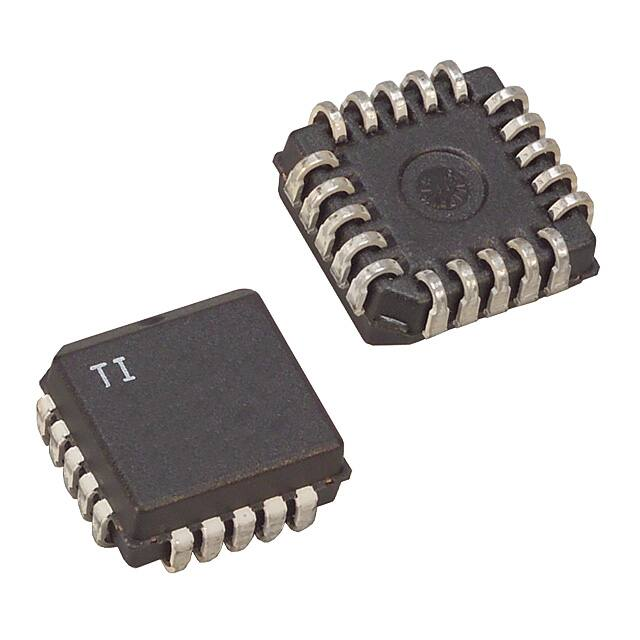
DB, DW, OR N PACKAGE
(TOP VIEW)
ANLG IN
(LSB) D0
D1
D2
D3
WR/RDY
MODE
RD
INT
GND
1
20
2
19
3
18
4
17
5
16
6
15
7
14
8
13
9
12
10
11
VCC
NC
OFLW
D7 (MSB)
D6
D5
D4
CS
REF +
REF –
FN PACKAGE
(TOP VIEW)
D1
D0 (LSB)
ANLG IN
VCC
NC
D
description
INT
GND
REF –
REF+
CS
The TLC0820AC and the TLC0820AI are
Advanced LinCMOS 8-bit analog-to-digital
converters each consisting of two 4-bit flash
3 2 1 20 19
D2
18 OFLW
4
converters, a 4-bit digital-to-analog converter, a
D3
17 D7 (MSB)
5
summing (error) amplifier, control logic, and a
WR/RDY
16 D6
6
result latch circuit. The modified flash technique
MODE
15 D5
7
allows low-power integrated circuitry to complete
RD
14 D4
8
an 8-bit conversion in 1.18 µs over temperature.
9 10 11 12 13
The on-chip track-and-hold circuit has a 100-ns
sample window and allows these devices to
convert continuous analog signals having slew
rates of up to 100 mV/µs without external
NC – No internal connection
sampling components. TTL-compatible 3-state
output drivers and two modes of operation allow
interfacing to a variety of microprocessors. Detailed information on interfacing to most popular microprocessors
is readily available from the factory.
AVAILABLE OPTIONS
PACKAGE
TA
TOTAL
UNADJUSTED
ERROR
SSOP
(DB)
0°C to 70°C
± 1 LSB
TLC0820ACDB
– 40°C to 85°C
± 1 LSB
—
PLASTIC
SMALL OUTLINE
(DW)
PLASTIC
CHIP CARRIER
(FN)
PLASTIC DIP
(N)
TLC0820ACDW
TLC0820ACFN
TLC0820ACN
TLC0820AIDW
TLC0820AIFN
TLC0820AIN
Advanced LinCMOS is a trademark of Texas Instruments Incorporated.
Copyright 1994, Texas Instruments Incorporated
PRODUCTION DATA information is current as of publication date.
Products conform to specifications per the terms of Texas Instruments
standard warranty. Production processing does not necessarily include
testing of all parameters.
POST OFFICE BOX 655303
• DALLAS, TEXAS 75265
2–1
�TLC0820AC, TLC0820AI
Advanced LinCMOS HIGH-SPEED 8-BIT ANALOG-TO-DIGITAL
CONVERTERS USING MODIFIED FLASH TECHNIQUES
SLAS064A – SEPTEMBER 1986 – REVISED JUNE 1994
functional block diagram
REF+
REF –
12
4-Bit Flash
Analog-to-Digital
Converter
(4 MSBs)
11
4
4
18
2
4
3
4
Output
Latch
and
3-State
Buffers
4-Bit
Digital-to-Analog
Converter
Summing
Amplifier
–1
ANLG IN
MODE
WR/RDY
CS
RD
2–2
1
4-Bit Flash
Analog-to-Digital
Converter
(4 LSBs)
5
14
15
16
4
17
OFLW
D0 (LSB)
D1
D2
D3
D4
D5
D6
D7 (MSB)
+1
7
6
Timing
and
Control
13
8
POST OFFICE BOX 655303
• DALLAS, TEXAS 75265
9
INT
Digital
Outputs
�TLC0820AC, TLC0820AI
Advanced LinCMOS HIGH-SPEED 8-BIT ANALOG-TO-DIGITAL
CONVERTERS USING MODIFIED FLASH TECHNIQUES
SLAS064A – SEPTEMBER 1986 – REVISED JUNE 1994
Terminal Functions
TERMINAL
NAME
ANLG IN
NO.
I/O
DESCRIPTION
1
I
Analog input
CS
13
I
Chip select. CS must be low in order for RD or WR to be recognized by the ADC.
D0
2
O
Digital, 3-state output data, bit 1 (LSB)
D1
3
O
Digital, 3-state output data, bit 2
D2
4
O
Digital, 3-state output data, bit 3
D3
5
O
Digital, 3-state output data, bit 4
D4
14
O
Digital, 3-state output data, bit 5
D5
15
O
Digital, 3-state output data, bit 6
D6
16
O
Digital, 3-state output data, bit 7
D7
17
O
Digital, 3-state output data, bit 8 (MSB)
GND
10
Ground
INT
9
O
Interrupt. In the write-read mode, the interrupt output (INT) going low indicates that the internal count-down delay
time, td(int), is complete and the data result is in the output latch. The delay time td(int) is typically 800 ns starting
after the rising edge of WR (see operating characteristics and Figure 3). If RD goes low prior to the end of td(int),
INT goes low at the end of td(RIL) and the conversion results are available sooner (see Figure 2). INT is reset by
the rising edge of either RD or CS.
MODE
7
I
Mode select. MODE is internally tied to GND through a 50-µA current source, which acts like a pulldown resistor.
When MODE is low, the read mode is selected. When MODE is high, the write-read mode is selected.
NC
19
OFLW
18
O
Overflow. Normally OFLW is a logical high. However, if the analog input is higher than Vref+, OFLW will be low at
the end of conversion. It can be used to cascade two or more devices to improve resolution (9 or 10 bits).
8
I
Read. In the write-read mode with CS low, the 3-state data outputs D0 through D7 are activated when RD goes
low. RD can also be used to increase the conversion speed by reading data prior to the end of the internal
count-down delay time. As a result, the data transferred to the output latch is latched after the falling edge of RD.
In the read mode with CS low, the conversion starts with RD going low. RD also enables the 3-state data outputs
on completion of the conversion. RDY going into the high-impedance state and INT going low indicate completion
of the conversion.
REF –
11
I
Reference voltage. REF – is placed on the bottom of the resistor ladder.
REF +
12
I
Reference voltage. REF + is placed on the top of the resistor ladder.
VCC
WR/RDY
20
RD
6
No internal connection
Power supply voltage
I/O
Write ready. In the write-read mode with CS low, the conversion is started on the falling edge of the WR input signal.
The result of the conversion is strobed into the output latch after the internal count-down delay time, td(int), provided
that the RD input does not go low prior to this time. The delay time td(int) is approximately 800 ns. In the read mode,
RDY (an open-drain output) goes low after the falling edge of CS and goes into the high-impedance state when
the conversion is strobed into the output latch. It is used to simplify the interface to a microprocessor system.
POST OFFICE BOX 655303
• DALLAS, TEXAS 75265
2–3
�TLC0820AC, TLC0820AI
Advanced LinCMOS HIGH-SPEED 8-BIT ANALOG-TO-DIGITAL
CONVERTERS USING MODIFIED FLASH TECHNIQUES
SLAS064A – SEPTEMBER 1986 – REVISED JUNE 1994
absolute maximum ratings over operating free-air temperature range (unless otherwise noted)†
Supply voltage, VCC (see Note 1) . . . . . . . . . . . . . . . . . . . . . . . . . . . . . . . . . . . . . . . . . . . . . . . . . . . . . . . . . . . 10 V
Input voltage range, all inputs (see Note 1) . . . . . . . . . . . . . . . . . . . . . . . . . . . . . . . . . . . . . – 0.2 V to VCC + 0.2 V
Output voltage range, all outputs (see Note 1) . . . . . . . . . . . . . . . . . . . . . . . . . . . . . . . . . . – 0.2 V to VCC + 0.2 V
Operating free-air temperature range: TLC0820AC . . . . . . . . . . . . . . . . . . . . . . . . . . . . . . . . . . . . . 0°C to 70°C
TLC0820AI . . . . . . . . . . . . . . . . . . . . . . . . . . . . . . . . . . . . – 40°C to 85°C
Storage temperature range . . . . . . . . . . . . . . . . . . . . . . . . . . . . . . . . . . . . . . . . . . . . . . . . . . . . . . . . – 65°C to 150°C
Case temperature for 10 seconds: FN package . . . . . . . . . . . . . . . . . . . . . . . . . . . . . . . . . . . . . . . . . . . . . . 260°C
Lead temperature 1,6 mm (1/16 inch) from case for 10 seconds: DB, DW or N package . . . . . . . . . . . 260°C
† Stresses beyond those listed under “absolute maximum ratings” may cause permanent damage to the device. These are stress ratings only, and
functional operation of the device at these or any other conditions beyond those indicated under “recommended operating conditions” is not
implied. Exposure to absolute-maximum-rated conditions for extended periods may affect device reliability.
NOTE 1: All voltages are with respect to network GND.
recommended operating conditions
MIN
NOM
MAX
Supply voltage, VCC
4.5
5
8
Analog input voltage
– 0.1
Positive reference voltage, Vref +
Vref –
GND
Negative reference voltage, Vref –
High level input voltage,
High-level
voltage VIH
VCC = 4.75
4 75 V to 5.25
5 25 V
Low level input voltage,
Low-level
voltage VIL
VCC = 4.75
4 75 V to 5.25
5 25 V
CS, WR/RDY, RD
MODE
Operating free-air
free air temperature,
temperature TA
2–4
Vref+
V
2
1.5
• DALLAS, TEXAS 75265
V
V
3.5
MODE
TLC0820AI
POST OFFICE BOX 655303
V
0.8
TLC0820AC
V
VCC + 0.1
VCC
CS, WR/RDY, RD
Pulse duration, write in write-read mode, tw(W) (see Figures 2, 3, and 4)
UNIT
0.5
50
0
70
– 40
85
V
µs
°C
�TLC0820AC, TLC0820AI
Advanced LinCMOS HIGH-SPEED 8-BIT ANALOG-TO-DIGITAL
CONVERTERS USING MODIFIED FLASH TECHNIQUES
SLAS064A – SEPTEMBER 1986 – REVISED JUNE 1994
electrical characteristics at specified operating free-air temperature, VCC = 5 V (unless otherwise
noted)
PARAMETER
VOH
VOL
Hi h l
High-level
l output
t t voltage
lt
Low level output voltage
Low-level
TA†
MIN
Full range
2.4
VCC = 4.75 V,,
IOH = – 10 µA
Full range
4.5
25°C
4.6
VCC = 5.25 V,,
IOL = 1.6 mA
Full range
0.4
25°C
0.34
TEST CONDITIONS
D0 – D7, INT, or
OFLW
D0 – D7, OFLW, INT,
or WR/RDY
VCC = 4.75 V,
IOH = – 360 µA
CS or RD
IIH
High-level input current
WR/RDY
Full range
VIH = 5 V
IIL
IOZ
Low-level input current
Off-state ((high-impedance-state)
g
)
output current
Full range
IOS
VI = 5 V
CS at 5 V
V,
VI = 0
VO = 5 V
D0 – D7 or OFLW
INT
Reference resistance
ICC
Supply current
Ci
Input capacitance
CS, WR/RDY, and
RD at 0 V
D0 – D7
170
– 0.005
–1
Co
Output capacitance
D0 – D7
† Full range is as specified in recommended operating conditions.
– 0.1
Full range
–3
25°C
– 0.3
25°C
8.4
–6
– 7.2
Full range
– 4.5
25°C
– 5.3
Full range
1.25
25°C
1.4
14
mA
– 12
–9
6
2.3
Full range
25°C
µA
7
Full range
25°C
µA
3
0.3
Full range
µA
– 0.3
25°C
Full range
• DALLAS, TEXAS 75265
0.3
–3
Full range
Full range
ANLG IN
POST OFFICE BOX 655303
50
0.1
25°C
CS at 5 V
V,
µA
3
25°C
VO = 0
Rreff
0.3
Full range
Analog input current
Short circuit output current
Short-circuit
0.1
Full range
D0 – D7 or WR/RDY
D0 – D7, OFLW, INT,
or WR/RDY
1
V
200
25°C
VO = 0
II
0.005
Full range
VO = 5 V
UNIT
3
25°C
VIL = 0
MAX
V
Full range
MODE
CS, WR/RDY, RD,
or MODE
TYP
5.3
15
7.5
13
5
kΩ
mA
pF
45
5
pF
2–5
�TLC0820AC, TLC0820AI
Advanced LinCMOS HIGH-SPEED 8-BIT ANALOG-TO-DIGITAL
CONVERTERS USING MODIFIED FLASH TECHNIQUES
SLAS064A – SEPTEMBER 1986 – REVISED JUNE 1994
operating characteristics, VCC = 5 V, Vref+ = 5 V, Vref– = 0, tr = tf = 20 ns, TA = 25°C (unless otherwise
noted)
PARAMETER
TEST CONDITIONS†
TYP
MAX
UNIT
± 1/16
± 1/4
LSB
1
LSB
See Figure 1
1.6
2.5
µs
tconv(R)
+ 20
tconv(R)
+ 50
ns
kSVS
Supply-voltage sensitivity
Total unadjusted error‡
VCC = 5 V ± 5%,
MODE at 0 V,
TA = MIN to MAX
TA = MIN to MAX
tconv(R)
Conversion time, read mode
MODE at 0 V,
MIN
ta(R)
Access time, RD↓ to data valid
MODE at 0 V,
See Figure 1
CL = 15 pF
280
Access time
time, RD↓ to data valid
MODE at 5 V,
td(WR) < td(i
d(int)),
See Figure 2
190
ta(R1)
(R1)
CL = 100 pF
210
320
CL = 15 pF
120
Access time
time, RD↓ to data valid
MODE at 5 V,
td(WR) > td(i
d(int)),
See Figure 3
70
ta(R2)
(R2)
CL = 100 pF
90
150
ta(INT)
Access time, INT↓ to data valid
MODE at 5 V,
See Figure 4
20
50
ns
tdis
Disable time,
time RD↑ to data valid
RL = 1 kΩ,
CL = 10 pF,
See Figures 1, 2, 3, and 5
70
95
ns
td(int)
Delay time
time, WR/RDY↑ to INT↓
MODE at 5 V,
CL = 50 pF,
See Figures 2, 3, and 4
800
1300
ns
td(NC)
Delay time, to next conversion
See Figures 1, 2, 3, and 4
500
ns
td(WR)
Delay time, WR/RDY↑ to RD↓ in
write-read mode
See Figure 2
0.4
µs
td(RDY)
time CS↓ to WR/RDY↓
Delay time,
MODE at 0 V,
See Figure 1
CL = 50 pF,
td(RIH)
Delay time, RD↑ to INT↑
CL = 50 pF,
td(RIL)
Delay time,
time RD↓ to INT↓
MODE at 5 V,
See Figure 2
td(WIH)
Delay time
time, WR/RDY↑ to INT↑
MODE at 5 V,
See Figure 4
ns
ns
50
100
ns
See Figures 1, 2, and 3
125
225
ns
td(WR) < td(int),
200
290
ns
CL = 50 pF,
175
270
ns
Slew-rate tracking
0.1
† For conditions shown as MIN or MAX, use the appropriate value specified under recommended operating conditions.
‡ Total unadjusted error includes offset, full-scale, and linearity errors.
2–6
POST OFFICE BOX 655303
• DALLAS, TEXAS 75265
V/µs
�TLC0820AC, TLC0820AI
Advanced LinCMOS HIGH-SPEED 8-BIT ANALOG-TO-DIGITAL
CONVERTERS USING MODIFIED FLASH TECHNIQUES
SLAS064A – SEPTEMBER 1986 – REVISED JUNE 1994
PARAMETER MEASUREMENT INFORMATION
CS
50%
RD
50%
50%
50%
td(NC)
WR/RDY
50%
With External Pullup
td(RDY)
td(RIH)
INT
50%
50%
tconv(R)
90%
10%
D0–D7
90%
10%
ta(R)
tdis
Figure 1. Read-Mode Waveforms (MODE Low)
CS
CS
tw(W)
tw(W)
WR/RDY 50%
50%
WR/RDY 50%
50%
td(WR)
50%
td(NC)
td(NC)
50%
RD
50%
RD
50%
50%
50%
50%
INT
90%
10%
90%
50%
td(int)
td(RIH)
td(int)
D0 – D7
td(RIH
td(WR)
td(RIL)
INT
50%
90%
10%
D0 – D7
10%
ta(R2)
ta(R1)
tdis
Figure 2. Write-Read-Mode Waveforms
[MODE High and td(WR) < td(int)]
POST OFFICE BOX 655303
90%
10%
tdis
Figure 3. Write-Read-Mode Waveforms
[MODE High and td(WR) > td(int)]
• DALLAS, TEXAS 75265
2–7
�TLC0820AC, TLC0820AI
Advanced LinCMOS HIGH-SPEED 8-BIT ANALOG-TO-DIGITAL
CONVERTERS USING MODIFIED FLASH TECHNIQUES
SLAS064A – SEPTEMBER 1986 – REVISED JUNE 1994
PARAMETER MEASUREMENT INFORMATION
CS Low
RD Low
tw(W)
WR/RDY
50%
50%
50%
td(WIH)
50%
INT
td(NC)
50%
td(int)
ta(INT)
90%
D0 – D7
Data Valid
10%
Figure 4. Write-Read-Mode Waveforms
(Stand-Alone Operation, MODE High, and RD Low)
VCC
CL = 10 pF
TLC0820
Input
tr
RD
Data
Output
Dn
CS
RD
GND
CL
VCC
90%
50%
10%
GND
tdis
1 kΩ
90%
Data
Outputs
VOH
GND
tr = 20 ns
TEST CIRCUIT
VOLTAGE WAVEFORMS
VCC
CL = 10 pF
tr
TLC0820
90%
50%
10%
1 kΩ
Input
RD
RD
Data
Output
Dn
CS
GND
GND
tdis
VCC
CL
Data
Outputs
10%
tr = 20 ns
VOLTAGE WAVEFORMS
Dn = D0 . . . D7
TEST CIRCUIT
Figure 5. Test Circuit and Voltage Waveforms
2–8
VCC
POST OFFICE BOX 655303
• DALLAS, TEXAS 75265
VOL
�TLC0820AC, TLC0820AI
Advanced LinCMOS HIGH-SPEED 8-BIT ANALOG-TO-DIGITAL
CONVERTERS USING MODIFIED FLASH TECHNIQUES
SLAS064A – SEPTEMBER 1986 – REVISED JUNE 1994
PRINCIPLES OF OPERATION
The TLC0820AC and TLC0820AI each employ a combination of sampled-data comparator techniques and flash
techniques common to many high-speed converters. Two 4-bit flash analog-to-digital conversions are used to give
a full 8-bit output.
The recommended analog input voltage range for conversion is – 0.1 V to VCC + 0.1 V. Analog input signals that are
less than Vref – + 1/2 LSB or greater than Vref+ – 1/2 LSB convert to 00000000 or 11111111, respectively. The reference
inputs are fully differential with common-mode limits defined by the supply rails. The reference input values define
the full-scale range of the analog input. This allows the gain of the ADC to be varied for ratiometric conversion by
changing the Vref+ and Vref – voltages.
The device operates in two modes, read (only) and write-read, that are selected by MODE. The converter is set to
the read (only) mode when MODE is low. In the read mode, WR/RDY is used as an output and is referred to as the
ready terminal. In this mode, a low on WR/RDY while CS is low indicates that the device is busy. Conversion starts
on the falling edge of RD and is completed no more than 2.5 µs later when INT falls and WR/RDY returns to the
high-impedance state. Data outputs also change from high-impedance to active states at this time. After the data is
read, RD is taken high, INT returns high, and the data outputs return to their high-impedance states.
When MODE is high, the converter is set to the write-read mode and WR/RDY is referred to as the write terminal.
Taking CS and WR/RDY low selects the converter and initiates measurement of the input signal. Approximately
600 ns after WR/RDY returns high, the conversion is completed. Conversion starts on the rising edge of WR/RDY
in the write-read mode.
The high-order 4-bit flash ADC measures the input by means of 16 comparators operating simultaneously. A
high-precision 4-bit DAC then generates a discrete analog voltage from the result of that conversion. After a time
delay, a second bank of comparators does a low-order conversion on the analog difference between the input level
and the high-order DAC output. The results from each of these conversions enter an 8-bit latch and are output to the
3-state output buffers on the falling edge of RD.
POST OFFICE BOX 655303
• DALLAS, TEXAS 75265
2–9
�TLC0820AC, TLC0820AI
Advanced LinCMOS HIGH-SPEED 8-BIT ANALOG-TO-DIGITAL
CONVERTERS USING MODIFIED FLASH TECHNIQUES
SLAS064A – SEPTEMBER 1986 – REVISED JUNE 1994
APPLICATION INFORMATION
CS
13
WR
6
RD
8
VCC
WR/RDY ANLG
IN
CS
20
5V
1
ANLG
IN
RD
TLC0820
µP
Bus
D0
2
D1
3
D2
4
D3
5
D4
14
D5
15
D6
16
D7
17
MODE
D0
D1
REF+
7
5V
12
5V
D2
0.1 µF
D3
D4
D5
REF –
11
D6
0.1 µF
D7
D8
18
OFL
13
6
8
OFLW
GND
VCC
WR/RDY ANLG
IN
CS
10
20
5V
1
RD
TLC0820
2
3
4
5
14
15
16
17
18
D0
D1
MODE
REF+
POST OFFICE BOX 655303
5V
12
D2
0.1 µF
D3
D4
D5
REF –
11
D6
D7
OFLW
GND
Figure 6. Configuration for 9-Bit Resolution
2–10
7
• DALLAS, TEXAS 75265
10
0.1 µF
�PACKAGE OPTION ADDENDUM
www.ti.com
14-Oct-2022
PACKAGING INFORMATION
Orderable Device
Status
(1)
Package Type Package Pins Package
Drawing
Qty
Eco Plan
(2)
Lead finish/
Ball material
MSL Peak Temp
Op Temp (°C)
Device Marking
(3)
Samples
(4/5)
(6)
TLC0820ACDB
ACTIVE
SSOP
DB
20
70
RoHS & Green
NIPDAU
Level-1-260C-UNLIM
TLC0820ACDBR
ACTIVE
SSOP
DB
20
2000
RoHS & Green
NIPDAU
TLC0820ACDW
ACTIVE
SOIC
DW
20
25
RoHS & Green
TLC0820ACDWR
ACTIVE
SOIC
DW
20
2000
TLC0820ACFN
ACTIVE
PLCC
FN
20
TLC0820ACN
ACTIVE
PDIP
N
TLC0820AIDW
ACTIVE
SOIC
TLC0820AIDWR
ACTIVE
TLC0820AIFN
TLC0820AIN
0 to 70
P0820A
Samples
Level-1-260C-UNLIM
P0820A
Samples
NIPDAU
Level-1-260C-UNLIM
TLC0820A
Samples
RoHS & Green
NIPDAU
Level-1-260C-UNLIM
TLC0820A
Samples
46
RoHS & Green
SN
Level-1-260C-UNLIM
TLC0820AC
Samples
20
20
RoHS &
Non-Green
NIPDAU
N / A for Pkg Type
TLC0820ACN
Samples
DW
20
25
RoHS & Green
NIPDAU
Level-1-260C-UNLIM
TLC0820AI
Samples
SOIC
DW
20
2000
RoHS & Green
NIPDAU
Level-1-260C-UNLIM
TLC0820AI
Samples
ACTIVE
PLCC
FN
20
46
RoHS & Green
SN
Level-1-260C-UNLIM
TLC0820AI
Samples
ACTIVE
PDIP
N
20
20
RoHS &
Non-Green
NIPDAU
N / A for Pkg Type
TLC0820AIN
Samples
(1)
The marketing status values are defined as follows:
ACTIVE: Product device recommended for new designs.
LIFEBUY: TI has announced that the device will be discontinued, and a lifetime-buy period is in effect.
NRND: Not recommended for new designs. Device is in production to support existing customers, but TI does not recommend using this part in a new design.
PREVIEW: Device has been announced but is not in production. Samples may or may not be available.
OBSOLETE: TI has discontinued the production of the device.
(2)
RoHS: TI defines "RoHS" to mean semiconductor products that are compliant with the current EU RoHS requirements for all 10 RoHS substances, including the requirement that RoHS substance
do not exceed 0.1% by weight in homogeneous materials. Where designed to be soldered at high temperatures, "RoHS" products are suitable for use in specified lead-free processes. TI may
reference these types of products as "Pb-Free".
RoHS Exempt: TI defines "RoHS Exempt" to mean products that contain lead but are compliant with EU RoHS pursuant to a specific EU RoHS exemption.
Green: TI defines "Green" to mean the content of Chlorine (Cl) and Bromine (Br) based flame retardants meet JS709B low halogen requirements of


 工商网监
湘ICP备2023018690号
工商网监
湘ICP备2023018690号
