Sample &
Buy
Product
Folder
Support &
Community
Tools &
Software
Technical
Documents
TLC59213, TLC59213A
SLVS867B – MAY 2009 – REVISED AUGUST 2015
TLC59213x 8-Bit Parallel In and Out Darlington Source Driver With Latch
1 Features
3 Description
•
The TLC59213 and TLC59213A are 8-bit source
drivers with input latch with CLK input and CLR to set
the output OFF. The TLC59213 and TLC59213A
have large output source currents up to 500 mA with
Darlington transistor and collectors tied to VCC. These
feature make the device optimum level of driving the
matrix of ink jet printer head, LEDs, and the scan-side
of resistor's matrix. The TLC59213 and TLC59213A
differ only in the Data Hold Time Specification (th).
1
•
•
•
•
•
•
•
•
Output Current on Each Channel
(IOUT Max = –500 mA)
VCE(sus) = 13.2 V
Input Compatible With TTL/5-V CMOS
Clear (CLR) and Clock (CLK) TTL/CMOS Control
Inputs
CLR Control Input to Off the Output
Darlington Source Driver
Clock Input Up to 1 MHz
Enhanced Hold Time (th) on TLC59213A
Temperature Range: –40°C to 85°C
The clamp diode is between output and ground for
switching inductive load.
All inputs are TTL/CMOS, which enable to any logiclevel inputs such as MCU, CPU or SN74LV594 (serial
to parallel) and the output enable LED matrix display.
It can also be used with another device sink driver
such as TLC59210, TLC59211 and TLC59212.
2 Applications
•
•
•
Lamp and Display (LED)
Hammer
Relay
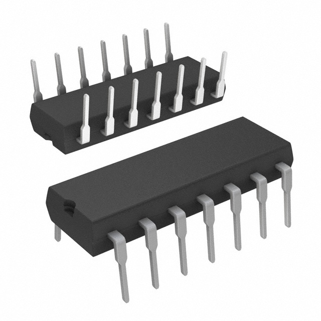
Device Information(1)
PART NUMBER
TLC59213
TLC59213A
PACKAGE
BODY SIZE (NOM)
PDIP (20)
24.33 mm × 6.35 mm
TSSOP (20)
6.50 mm × 4.40 mm
(1) For all available packages, see the orderable addendum at
the end of the data sheet.
Y7
Y8
D7
D8
Y6
Y5
Y4
Y3
Y2
Y1
VCC
Typical Application Diagram÷
CLK
D6
D5
D4
D3
D2
D1
CLR
TLC59213
MCU
1
An IMPORTANT NOTICE at the end of this data sheet addresses availability, warranty, changes, use in safety-critical applications,
intellectual property matters and other important disclaimers. PRODUCTION DATA.
�TLC59213, TLC59213A
SLVS867B – MAY 2009 – REVISED AUGUST 2015
www.ti.com
Table of Contents
1
2
3
4
5
6
7
8
Features ..................................................................
Applications ...........................................................
Description .............................................................
Revision History.....................................................
Pin Configuration and Functions .........................
Specifications.........................................................
1
1
1
2
3
4
6.1
6.2
6.3
6.4
6.5
6.6
6.7
4
4
4
4
5
5
5
Absolute Maximum Ratings .....................................
ESD Ratings ............................................................
Recommended Operating Conditions.......................
Electrical Characteristics...........................................
Timing Requirements ................................................
Switching Characteristics ..........................................
Typical Characteristics ..............................................
Parameter Measurement Information .................. 6
Detailed Description .............................................. 7
8.1 Overview ................................................................... 7
8.2 Functional Block Diagram ......................................... 7
8.3 Feature Description................................................... 7
8.4 Device Functional Modes.......................................... 7
9
Application and Implementation .......................... 8
9.1 Application Information.............................................. 8
9.2 Typical Application ................................................... 8
10 Power Supply Recommendations ....................... 9
11 Layout................................................................... 10
11.1 Layout Guidelines ................................................. 10
11.2 Layout Example .................................................... 10
12 Device and Documentation Support ................. 11
12.1
12.2
12.3
12.4
Community Resources..........................................
Trademarks ...........................................................
Electrostatic Discharge Caution ............................
Glossary ................................................................
11
11
11
11
13 Mechanical, Packaging, and Orderable
Information ........................................................... 11
4 Revision History
NOTE: Page numbers for previous revisions may differ from page numbers in the current version.
Changes from Revision A (March 2010) to Revision B
•
2
Page
Added Pin Configuration and Functions section, ESD Ratings table, Feature Description section, Device Functional
Modes, Application and Implementation section, Power Supply Recommendations section, Layout section, Device
and Documentation Support section, and Mechanical, Packaging, and Orderable Information section .............................. 1
Submit Documentation Feedback
Copyright © 2009–2015, Texas Instruments Incorporated
Product Folder Links: TLC59213 TLC59213A
�TLC59213, TLC59213A
www.ti.com
SLVS867B – MAY 2009 – REVISED AUGUST 2015
5 Pin Configuration and Functions
N or PW Package
20-Pin PDIP or TSSOP
Top View
CLR
D1
D2
D3
D4
D5
D6
D7
D8
CLK
1
20
VCC
2
19
3
18
Y1
Y2
Y3
Y4
Y5
Y6
Y7
Y8
GND
4
17
5
16
6
15
7
14
8
13
9
12
10
11
Pin Functions
PIN
NAME
NO.
I/O
DESCRIPTION
CLR
1
I
Direct clear of output
D1
2
I
Input control to the current source driver
D2
3
I
Input control to the current source driver
D3
4
I
Input control to the current source driver
D4
5
I
Input control to the current source driver
D5
6
I
Input control to the current source driver
D6
7
I
Input control to the current source driver
D7
8
I
Input control to the current source driver
D8
9
I
Input control to the current source driver
CLK
10
I
Clock to positive edge triggered D flipflops
GND
11
—
Ground
Y8
12
O
Output to load
Y7
13
O
Output to load
Y6
14
O
Output to load
Y5
15
O
Output to load
Y4
16
O
Output to load
Y3
17
O
Output to load
Y2
18
O
Output to load
Y1
19
O
Output to load
Vcc
20
I
Supply voltage
Copyright © 2009–2015, Texas Instruments Incorporated
Product Folder Links: TLC59213 TLC59213A
Submit Documentation Feedback
3
�TLC59213, TLC59213A
SLVS867B – MAY 2009 – REVISED AUGUST 2015
www.ti.com
6 Specifications
6.1 Absolute Maximum Ratings (1)
over operating free-air temperature range (unless otherwise noted)
MIN
MAX
UNIT
VDD
Supply voltage
–0.5
15
V
VI
Input voltage
–0.5
VCC + 0.5
V
Collector-emitter voltage
–0.5
15
V
–500
mA
IO
Peak output current
IIK
Input clamp current
VI < 0 V
–20
mA
IOK
Output clamp current
VO < 0 V
–500
mA
Tstg
Storage temperature
150
°C
(1)
–65
Stresses beyond those listed under Absolute Maximum Ratings may cause permanent damage to the device. These are stress ratings
only, which do not imply functional operation of the device at these or any other conditions beyond those indicated under Recommended
Operating Conditions. Exposure to absolute-maximum-rated conditions for extended periods may affect device reliability.
6.2 ESD Ratings
VALUE
V(ESD)
(1)
(2)
Electrostatic discharge
Human body model (HBM), per ANSI/ESDA/JEDEC JS-001 (1)
±2000
Charged-device model (CDM), per JEDEC specification JESD22C101 (2)
±1000
UNIT
V
JEDEC document JEP155 states that 500-V HBM allows safe manufacturing with a standard ESD control process.
JEDEC document JEP157 states that 250-V CDM allows safe manufacturing with a standard ESD control process.
6.3 Recommended Operating Conditions
VCC
Supply voltage
VIH
High-level input voltage
VIL
Low-level input voltage
UNIT
13.2
V
V
0.8
Output current (8 channel)
PW package
TA
MAX
4.5
2
N package
IO
MIN
Duty cycle < 10%
400
Duty cycle < 50%
200
Duty cycle < 10%
350
Duty cycle < 50%
V
mA
170
Operating free-air temperature
–40
85
°C
6.4 Electrical Characteristics
over recommended operating free-air temperature range (unless otherwise noted)
PARAMETER
ICEX
VCE(sus)
Output leakage current
Output saturation voltage
TEST CONDITIONS
MAX
IOUT = –350 mA
2.35
IOUT = –225 mA
2.15
IOUT = –100 mA
1.96
Input current
VCC = 13.2 V, VI = 0 or 13.2 V
Vf
Clamp forward voltage
If = –350 mA
ICC
Supply current
VCC = 13.2 V,
VI = 0 or 13.2 V
CI
Input capacitance
Submit Documentation Feedback
TYP
2
II
4
MIN
VCC = 13.2 V, Outputs off
1
–2
UNIT
µA
V
µA
V
All outputs OFF
4.6
13
All outputs ON
4.8
13
10
mA
pF
Copyright © 2009–2015, Texas Instruments Incorporated
Product Folder Links: TLC59213 TLC59213A
�TLC59213, TLC59213A
www.ti.com
SLVS867B – MAY 2009 – REVISED AUGUST 2015
6.5 Timing Requirements
over recommended operating free-air temperature range (unless otherwise noted), see Figure 3
MIN
tsu
th
Setup time
50
ns
CLR high before CLK ↑
50
ns
TLC59213,
TLC59213A
TA = -40°C to 85°C
50
TLC59213
TA = 0°C to 70°C
25
TA = 0°C to 70°C, VCC = 4.5 V to 5.5 V
15
TA = 0°C to 70°C, VCC = 10.8 V to 13.2 V
19
TLC59213A
tw
Pulse width
UNIT
D before CLK ↑
D after CLK ↑
Hold time
MAX
CLK, CLR
ns
100
ns
6.6 Switching Characteristics
over operating free-air temperature range (unless otherwise noted), see Figure 3
PARAMETER
FROM
(INPUT)
TO
(OUTPUT)
TEST
CONDITIONS
TA = 25°C
MIN
TA = –40°C to 85°C
TYP MAX
MIN
UNIT
MAX
tPLH
Propagation delay time,
low-to-high level output
CLK
Y
RL = 25 Ω,
CL = 15 pF
107
200
250
ns
tPHL
Propagation delay time,
high-to-low level output
CLK
Y
RL = 25 Ω,
CL = 15 pF
111
200
250
ns
tPHLR
Propagation delay time,
high-to-low level output
CLR
Y
RL = 25 Ω,
CL = 15 pF
104
200
250
ns
6.7 Typical Characteristics
550
550
TA = 85°C
450
400
350
N=1
N=2
300
N=3
250
200
150
N=8
N=7
100
N=6 N=5
50
TA = 85°C
500
N = Number of outputs
conducting
simultaneously
Maximum Output Current, IO (mA)
Maximum Output Current, IO (mA)
500
N = Number of outputs
conducting
simultaneously
450
400
350
N=2
N=3
250
200
150
N=8
N=7
100
N=6 N=5
50
N=4
0
N=1
300
N=4
0
0
10
20
30
40 50 60
Duty Cycle (%)
70
80
90
100
Figure 1. Maximum Output Current vs Duty Cycle (TSSOP
(PW) Package)
0
10
20
30
40 50 60
Duty Cycle (%)
70
80
90
100
Figure 2. Maximum Output Current vs Duty Cycle (DIP (N)
Package)
Copyright © 2009–2015, Texas Instruments Incorporated
Product Folder Links: TLC59213 TLC59213A
Submit Documentation Feedback
5
�TLC59213, TLC59213A
SLVS867B – MAY 2009 – REVISED AUGUST 2015
www.ti.com
7 Parameter Measurement Information
Test Point
From Output
Under Test
RL = 25 Ω
CL
(See Note A)
TEST CIRCUIT
3V
CLR
1.5 V
tsu
GND
3V
1.5 V
D
1.5 V
tsu
GND
th
tf
tr
90%
1.5 V
10%
90%
tw
3V
1.5 V
10%
tPLH
50%
CLK
GND
tPHL
VOH
50%
50%
Y
GND
VOLTAGE WAVEFORMS
A.
CL includes probe and jig capacitance.
B.
All input pulses are supplied by generators having the following characteristics: PRR ≤ 1 MHz, ZO = 50 Ω, tr ≤ 3 ns,
and tf ≤ 3 ns.
C.
The outputs are measured one at a time with one transition per measurement.
Figure 3. Test Circuit and Voltage Waveforms
6
Submit Documentation Feedback
Copyright © 2009–2015, Texas Instruments Incorporated
Product Folder Links: TLC59213 TLC59213A
�TLC59213, TLC59213A
www.ti.com
SLVS867B – MAY 2009 – REVISED AUGUST 2015
8 Detailed Description
8.1 Overview
The TLC59213 device is an 8-bit Darlington source driver with latch for large-output source currents up to
500 mA.
8.2 Functional Block Diagram
VCC
Y1
Y2
Y3
Y4
Y5
Y6
Y7
Y8
20
19
18
17
16
15
14
13
12
CLR 1
CLK 10
Q_
D
(1)
R
CK
Q_
D
Q_
R
CK
D
R
CK
Q_
D
Q_
R
CK
D
Q_
R
CK
D
R
CK
Q_
D
R
CK
Q_
D
R
CK
2
3
4
5
6
7
8
9
11
D1
D2
D3
D4
D5
D6
D7
D8
GND
This symbol is in accordance with ANSI/IEEE Standard 91-1984 and IEC Publication 617-12.
8.3 Feature Description
Each of the 8 channels is controlled by its input (Dn), a direct clear (CLR), and clock (CLK) through a positiveedge-triggered D-type flip-flops. Information at the data (D) input meeting the setup time requirements is
transferred to the output (Y) on the positive-going edge of the clock (CLK) pulse. When CLK is at either the high
or low level, the D-input has no effect at the output. When CLR is at low level, the D-input has no effect at the
output.
8.4 Device Functional Modes
Table 1 lists the functional modes of the TLC59213.
Table 1. Function Table (Each Latch) (1)
INPUTS
(1)
OUTPUT
Y
CLR
CLK
D
L
X
X
Z (OFF)
H
↑
L
Z (OFF)
H
↑
H
H (ON)
H
L
X
Y0
H
↓
X
Y0
L: Low-level
H: High-level
X: Irrelevant
↑: Rising edge
↓: Falling edge
Z : High-impedance (OFF)
Copyright © 2009–2015, Texas Instruments Incorporated
Product Folder Links: TLC59213 TLC59213A
Submit Documentation Feedback
7
�TLC59213, TLC59213A
SLVS867B – MAY 2009 – REVISED AUGUST 2015
www.ti.com
9 Application and Implementation
NOTE
Information in the following applications sections is not part of the TI component
specification, and TI does not warrant its accuracy or completeness. TI’s customers are
responsible for determining suitability of components for their purposes. Customers should
validate and test their design implementation to confirm system functionality.
9.1 Application Information
In LED display application, TLC59213 is used to drive the current source for 8 LEDs in parallel. LED display
pattern can be created by providing different bit pattern. At every positive clock edge, new bit pattern will be
transferred to LED display.
Y7
Y8
D7
D8
Y6
Y5
Y4
Y3
Y2
Y1
VCC
9.2 Typical Application
CLK
D6
D5
D4
D3
D2
D1
CLR
TLC59213
MCU
Figure 4. Typical Application Diagram
9.2.1 Design Requirements
For LED display application, LED is selected based on the application. The current level is determined by the
required brightness. Given the available supply, the resistor value could be determined. The maximum output
current is constrained by the duty cycle. See Figure 1 and Figure 2.
9.2.2 Detailed Design Procedure
The selection of supply voltage (VCC), LED, and resistor sets the current of the LED.
VR + VL + VCE = VCC
I = (VCC - VL - VCE) /R
(1)
(2)
VR is the voltage drop across the resistor, VL is the voltage drop across the LED when LED is on, VCE is the
collector-to-emitter voltage of the Darlington current source driver, when the driver is enabled. For example,
when VCC = 12 V, VL = 2.9 V, and VCE = 1.6 V, a 75-Ω resistor is used to obtain output current 100 mA.
8
Submit Documentation Feedback
Copyright © 2009–2015, Texas Instruments Incorporated
Product Folder Links: TLC59213 TLC59213A
�TLC59213, TLC59213A
www.ti.com
SLVS867B – MAY 2009 – REVISED AUGUST 2015
Typical Application (continued)
9.2.3 Application Curve
Figure 5. Output Voltage and Current Response
10 Power Supply Recommendations
The supply voltage to TLC59213 is from 4.5 V to 13.2 V.
Copyright © 2009–2015, Texas Instruments Incorporated
Product Folder Links: TLC59213 TLC59213A
Submit Documentation Feedback
9
�TLC59213, TLC59213A
SLVS867B – MAY 2009 – REVISED AUGUST 2015
www.ti.com
11 Layout
11.1 Layout Guidelines
The traces that carry current from the output pins must be wide enough to support the current.
11.2 Layout Example
To MCU
VCC
CLR
To MCU
D1
Y1
To MCU
D2
Y2
To MCU
D3
Y3
To MCU
D4
Y4
To MCU
D5
Y5
To MCU
D6
Y6
To MCU
D7
Y7
To MCU
D8
Y8
To MCU
CLK
VCC
GND
VIA to GND
Figure 6. Layout Recommendation
10
Submit Documentation Feedback
Copyright © 2009–2015, Texas Instruments Incorporated
Product Folder Links: TLC59213 TLC59213A
�TLC59213, TLC59213A
www.ti.com
SLVS867B – MAY 2009 – REVISED AUGUST 2015
12 Device and Documentation Support
12.1 Community Resources
The following links connect to TI community resources. Linked contents are provided "AS IS" by the respective
contributors. They do not constitute TI specifications and do not necessarily reflect TI's views; see TI's Terms of
Use.
TI E2E™ Online Community TI's Engineer-to-Engineer (E2E) Community. Created to foster collaboration
among engineers. At e2e.ti.com, you can ask questions, share knowledge, explore ideas and help
solve problems with fellow engineers.
Design Support TI's Design Support Quickly find helpful E2E forums along with design support tools and
contact information for technical support.
12.2 Trademarks
E2E is a trademark of Texas Instruments.
All other trademarks are the property of their respective owners.
12.3 Electrostatic Discharge Caution
These devices have limited built-in ESD protection. The leads should be shorted together or the device placed in conductive foam
during storage or handling to prevent electrostatic damage to the MOS gates.
12.4 Glossary
SLYZ022 — TI Glossary.
This glossary lists and explains terms, acronyms, and definitions.
13 Mechanical, Packaging, and Orderable Information
The following pages include mechanical, packaging, and orderable information. This information is the most
current data available for the designated devices. This data is subject to change without notice and revision of
this document. For browser-based versions of this data sheet, refer to the left-hand navigation.
Copyright © 2009–2015, Texas Instruments Incorporated
Product Folder Links: TLC59213 TLC59213A
Submit Documentation Feedback
11
�PACKAGE OPTION ADDENDUM
www.ti.com
10-Dec-2020
PACKAGING INFORMATION
Orderable Device
Status
(1)
Package Type Package Pins Package
Drawing
Qty
Eco Plan
(2)
Lead finish/
Ball material
MSL Peak Temp
Op Temp (°C)
Device Marking
(3)
(4/5)
(6)
TLC59213AIN
ACTIVE
PDIP
N
20
20
RoHS &
Non-Green
NIPDAU
N / A for Pkg Type
-40 to 85
TLC59213AIN
TLC59213AIPW
ACTIVE
TSSOP
PW
20
70
RoHS & Green
NIPDAU
Level-1-260C-UNLIM
TLC59213AIPWR
ACTIVE
TSSOP
PW
20
2000
RoHS & Green
NIPDAU
Level-1-260C-UNLIM
-40 to 85
Y59213A
TLC59213AIPWT
ACTIVE
TSSOP
PW
20
250
RoHS & Green
NIPDAU
Level-1-260C-UNLIM
-40 to 85
Y59213A
TLC59213IN
ACTIVE
PDIP
N
20
20
RoHS &
Non-Green
NIPDAU
N / A for Pkg Type
-40 to 85
TLC59213IN
TLC59213IPWR
ACTIVE
TSSOP
PW
20
2000
RoHS & Green
NIPDAU
Level-1-260C-UNLIM
-40 to 85
Y59213
Y59213A
(1)
The marketing status values are defined as follows:
ACTIVE: Product device recommended for new designs.
LIFEBUY: TI has announced that the device will be discontinued, and a lifetime-buy period is in effect.
NRND: Not recommended for new designs. Device is in production to support existing customers, but TI does not recommend using this part in a new design.
PREVIEW: Device has been announced but is not in production. Samples may or may not be available.
OBSOLETE: TI has discontinued the production of the device.
(2)
RoHS: TI defines "RoHS" to mean semiconductor products that are compliant with the current EU RoHS requirements for all 10 RoHS substances, including the requirement that RoHS substance
do not exceed 0.1% by weight in homogeneous materials. Where designed to be soldered at high temperatures, "RoHS" products are suitable for use in specified lead-free processes. TI may
reference these types of products as "Pb-Free".
RoHS Exempt: TI defines "RoHS Exempt" to mean products that contain lead but are compliant with EU RoHS pursuant to a specific EU RoHS exemption.
Green: TI defines "Green" to mean the content of Chlorine (Cl) and Bromine (Br) based flame retardants meet JS709B low halogen requirements of


 工商网监
湘ICP备2023018690号
工商网监
湘ICP备2023018690号
