TLC5923
DAP
RHB
www.ti.com
SLVS550B – DECEMBER 2004 – REVISED JANUARY 2013
16-CHANNEL LED DRIVER WITH DOT CORRECTION
Check for Samples: TLC5923
FEATURES
– TEF: Thermal Error Flag
1
•
•
2
•
•
•
•
•
•
•
•
•
•
•
•
16 Channels
Drive Capability
– 0 to 80 mA (Constant-Current Sink)
Constant Current Accuracy: ±1% (typical)
Serial Data Interface
Fast Switching Output: Tr / Tf = 10ns (typical)
CMOS Level Input/Output
30 MHz Data Transfer Rate
VCC = 3.0 V to 5.5 V
Operating Temperature = –40°C to 85°C
LED Supply Voltage up to 17 V
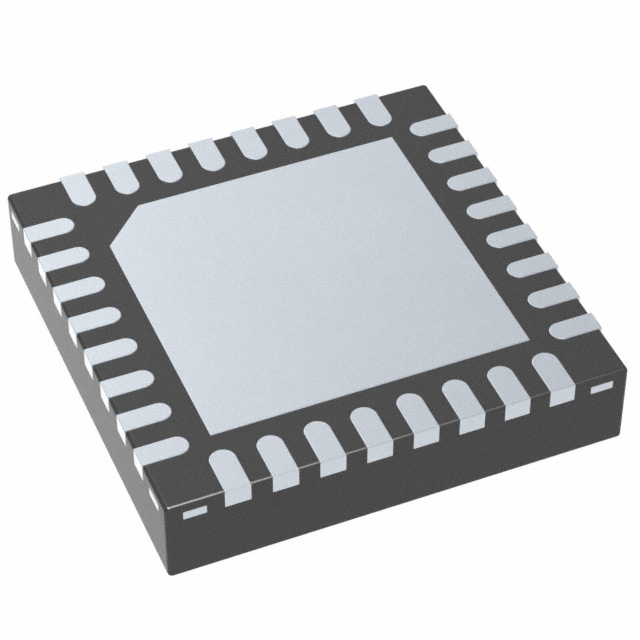
32-pin HTSSOP( PowerPAD™) and QFN
Packages
Dot Correction
– 7 bit (128 Steps)
– individual adjustable for each channel
Controlled In-Rush Current
Error Information
– LOD: LED Open Detection
APPLICATIONS
•
•
•
•
Monocolor, Multicolor, Fullcolor LED Display
Monocolor, Multicolor LED Signboard
Display Backlighting
Multicolor LED lighting applications
DESCRIPTION
The TLC5923 is a 16 channel constant-current sink
driver. Each channel has a On/Off state and a 128step adjustable constant current sink (dot correction).
The dot correction adjusts the brightness variations
between LED, LED channels and other LED drivers.
Both dot correction and On/Off state are accessible
via a serial data interface. A single external resistor
sets the maximum current of all 16 channels.
The TLC5923 features two error information circuits.
The LED open detection (LOD) indicates a broken or
disconnected LED at an output terminal. The thermal
error flag (TEF) indicates an overtemperature
condition.
FUNCTIONAL BLOCK DIAGRAM
VCC
GND PGND SCLK
SIN
MODE
XLAT
BLANK
MODE
0
1
1
LOD
0
0
On/Off Register
0
IREF
0
Max. OUTn
Current
Constant Current
Driver
Delay
x0
OUT0
0
7−bit DC Register
6
On/Off
Input
Shift
Register
BLANK
16
LOD
1
16
1
On/Off Register
15
0
LED Open
Detection
(LOD)
Constant Current
Driver
Delay
x1
OUT1
112
7
7−bit DC Register
13
DC Input
Shift
Register
BLANK
Temperature
Error Flag
(TEF)
BLANK
1 0
LOD
111
XERR
0
1
MODE
15
15
On/Off Register
Constant Current
Driver
Delay
x15
OUT15
105
7−bit DC Register
111
SOUT
1
2
Please be aware that an important notice concerning availability, standard warranty, and use in critical applications of
Texas Instruments semiconductor products and disclaimers thereto appears at the end of this data sheet.
PowerPAD is a trademark of Texas Instruments.
PRODUCTION DATA information is current as of publication date.
Products conform to specifications per the terms of the Texas
Instruments standard warranty. Production processing does not
necessarily include testing of all parameters.
Copyright © 2004–2013, Texas Instruments Incorporated
�TLC5923
SLVS550B – DECEMBER 2004 – REVISED JANUARY 2013
www.ti.com
This integrated circuit can be damaged by ESD. Texas Instruments recommends that all integrated circuits be handled with
appropriate precautions. Failure to observe proper handling and installation procedures can cause damage.
ESD damage can range from subtle performance degradation to complete device failure. Precision integrated circuits may be more
susceptible to damage because very small parametric changes could cause the device not to meet its published specifications.
ORDERING INFORMATION (1)
TA
–40°C to 85°C
(1)
Part Number (1)
Package
32-pin, HTSSOP, PowerPAD™
TLC5923DAP
32-pin, 5 mm x 5 mm QFN
TLC5923RHB
For the most current package and ordering information, see the Package Option Addendum at the end
of this document, or see the TI website at www.ti.com.
ABSOLUTE MAXIMUM RATINGS
(1) (2)
TLC5923
VCC
Supply voltage (2)
IO
Output current (dc)
I(OUT0) to I(OUT15)
VI
Input voltage range (2)
VO
Output voltage range (2)
Tstg
(2)
(3)
mA
V(BLANK), V(XLAT), V(SCLK), V(SIN), V(MODE), V(IREF)
–0.3 to VCC + 0.3
V
V(SOUT), V(XERR)
–0.3 to VCC + 0.3
V
-0.3 to 18
V
2
kV
HBM (JEDEC JESD22-A114, Human Body Model)
CDM (JEDEC JESD22-C101, Charged Device Model)
500
V
–40 to 150
°C
HTSSOP (DAP)
42.54
mW/°C
QFN (RHB)
27.86
mW/°C
Storage temperature range
Power dissipation rating at (or
above) TA = 25°C (3)
(1)
V
90
V(OUT0) to V(OUT15)
ESD rating
UNIT
–0.3 to 6
Stresses beyond those listed under absolute maximum ratings may cause permanent damage to the device. These are stress ratings
only, and functional operation of the device at these or any other conditions beyond those indicated under recommended operating
conditions is not implied. Exposure to absolute-maximum-rated conditions for extended periods may affect device reliability.
All voltage values are with respect to network ground terminal.
See SLMA002 for more information about PowerPAD™
RECOMMENDED OPERATING CONDITIONS—DC Characteristics
MIN
VCC
Supply voltage
VO
Voltage applied to output, (Out0 - Out15)
VIH
NOM
MAX
UNIT
3
5.5
V
17
V
High-level input voltage
0.8 VCC
VCC
V
VIL
Low-level input voltage
GND
0.2 VCC
V
IOH
High-level output current
VCC = 5 V at SOUT
IOL
Low-level output current
VCC = 5 V at SOUT, XERR
IOLC
Constant output current
OUT0 to OUT15
TA
Operating free-air temperature range
2
-40
Submit Documentation Feedback
–1
mA
1
mA
80
mA
85
°C
Copyright © 2004–2013, Texas Instruments Incorporated
Product Folder Links: TLC5923
�TLC5923
www.ti.com
SLVS550B – DECEMBER 2004 – REVISED JANUARY 2013
RECOMMENDED OPERATING CONDITIONS—AC Characteristics
VCC = 3 V to 5.5 V, TA = -40°C to 85°C (unless otherwise noted)
MIN
fSCLK
Clock frequency
TYP
SCLK
MAX
UNIT
30
MHz
twh0, twl0 CLK pulse duration
SCLK=H/L
16
ns
twh1
XLAT=H
20
ns
SIN to SCLK↑ (1)
10
SLCK↑ to XLAT↓(dot correction data)
10
SCLK↑to XLAT↑ (ON/OFF data)
10
tsu2
MODE↑↓ to SCLK↑
10
tsu3
MODE↑↓ to XLAT↑
10
th0
SCLK↑ to SIN
10
th1
XLAT ↓ to SCLK↑ (dot correction data)
10
XLAT pulse duration
tsu0
tsu1
tsu1a
th1a
Setup time
XLAT↑ to SCLK↑ (ON/OFF data)
10
th2
SCLK↑to MODE↑↓
10
th3
XLAT↓ to MODE↑↓
10
(1)
Hold time
ns
ns
"↑" and "↓" indicates a rising edge, and a falling edge respectively.
ELECTRICAL CHARACTERISTICS
VCC = 3 V to 5.5 V, TA = –40°C to 85°C (unless otherwise noted)
PARAMETER
TEST CONDITIONS
MIN
VOH
High-level output voltage
IOH = –1 mA, SOUT
VOL
Low-level output voltage
IOL = 1 mA, SOUT
II
Input current
VI = VCC or GND, BLANK, XLAT, SCLK, SIN, MODE
TYP
Supply current
–1
ILO0
0.5
V
1
μA
6
No data transfer, All output OFF, VO = 1 V, R(IREF) = 1.3
kΩ
15
Data transfer 30 MHz, All output ON, VO = 1 V,
R(IREF) = 1.3 kΩ
32
Data transfer 30 MHz, All output ON, VO = 1 V,
R(IREF) = 600 Ω
IOLC
Constant sink current
All output ON, VO = 1 V, R(IREF) = 600 Ω
Leakage output current
All output OFF, VO = 15 V, R(IREF) = 600 Ω, OUT0 to
OUT15
UNIT
V
No data transfer, All output OFF, VO = 1 V, R(IREF) = 10 kΩ
ICC
MAX
VCC –0.5
70
mA
36
65 (1)
80
90
mA
0.1
μA
10
μA
ILO1
VXERR = 5.5 V, No TEF and LOD
ΔIOLC0 Constant sink current error
All output ON, VO = 1 V, R(IREF) = 600 Ω, OUT0 to OUT15
±1%
±4%
ΔIOLC1 Constant sink current error
device to device, averaged current from OUT0 to OUT15,
R(IREF) = 600 Ω
±4%
±8.5%
ΔIOLC2 Line regulation
All output ON, VO = 1 V, R(IREF) = 600 Ω,
OUT0 to OUT15, VCC = 3 V to 5.5 V
±1
±4
%/V
ΔIOLC3 Load regulation
All output ON, VO = 1 V to 3 V, R(IREF) = 600 Ω,
OUT0 to OUT15
±2
±6
%/V
150
160
180
°C
0.3
0.4
V
1.20
1.24
1.28
V
T(TEF)
Thermal error flag threshold
V(LOD)
LED open detection threshold
V(IREF) Reference voltage output
(1)
(2)
Junction temperature, rising temperature
(2)
R(IREF) = 600 Ω
Measured at device start-up temperature. Once the IC is operating (self heating), lower ICC values will be seen. See Figure 18.
Not tested. Specified by design.
Submit Documentation Feedback
Copyright © 2004–2013, Texas Instruments Incorporated
Product Folder Links: TLC5923
3
�TLC5923
SLVS550B – DECEMBER 2004 – REVISED JANUARY 2013
www.ti.com
DISSIPATION RATINGS
PACKAGE
POWER RATING
TA < 25°C
DERATING FACTOR
ABOVE TA = 25°C
POWER RATING
TA = 70°C
POWER RATING
TA = 85°C
32-pin HTSSOP with PowerPAD (1)
soldered
5318 mW
42.54 mW/°C
3403 mW
2765 mW
32-pin HTSSOP with PowerPAD (1)
unsoldered
2820 mW
22.56 mW/°C
1805 mW
1466 mW
32-pin QFN
3482 mW
27.86 mW/°C
2228 mW
1811 mW
(1)
The PowerPAD is soldered to the PCB with a 2 oz. copper trace. See SLMA002 for further information.
SWITCHING CHARACTERISTICS
PARAMETER
tr0
tr1
tf0
tf1
TEST CONDITIONS
SOUT(see
Rise time
SOUT (see
(2)
)
10
30
30
(3)
30
)
)
(5)
BLANK ↑↓ to OUT0↑↓ (see
), Sink current On/Off
XLAT↑ to OUT0↑↓ (see
(5)
tpd4
OUTn↑↓ to XERR↑↓ (see
(6)
tpd5
XLAT↑ to IOUT(dot-correction) (see
60
)
60
)
UNIT
ns
ns
ns
1000
(7)
)
1000
OUTn↑ to OUT(n+1)↑, OUTn ↓ to OUT(n+1)↓ (see
Output delay time
30
(3) (4)
MODE↑↓ to SOUT↑↓ (see
(1)
(2)
(3)
(4)
(5)
(6)
(7)
10
16
tpd1
td
)
)
OUTn, VCC = 5 V, TA = 60°C, DCx = 7F (see
Propagation delay time
(2)
(1)
SCLK↑ to SOUT↑ ↓ (see
tpd3
MAX
16
tpd0
tpd2
TYP
)
OUTn, VCC = 5 V, TA = 60°C, DCx = 7F (see
Fall time
MIN
(1)
(5)
)
14
22
30
ns
See Figure 4. Defined as from 10% to 90%
See Figure 5. Defined as from 10% to 90%
See Figure 4, Figure 14
"↑" and "↓" indicates a rising edge, and a falling edge respectively.
See Figure 5 and Figure 14
See Figure 5, Figure 6, and Figure 14
See Figure 5
4
17 OUT11
18 OUT12
19 OUT13
20 PGND
21 OUT14
XERR
25
16
OUT10
MODE
26
15
PGND
IREF
27
14
OUT9
13
OUT8
12
OUT7
THERMAL
PAD
(QFN)
29
BLANK
30
11
OUT6
XLAT
31
10
PGND
SCLK
32
9
OUT5
Submit Documentation Feedback
OUT3 7
OUT4 8
28
PGND 5
OUT2 6
VCC
GND
OUT1 4
VCC
IREF
MODE
XERR
SOUT
PGND
OUT15
OUT14
PGND
OUT13
OUT12
OUT11
OUT10
PGND
OUT9
OUT8
22 OUT15
32
31
30
29
28
27
26
25
24
23
22
21
20
19
18
17
OUT0 3
1
2
3
4
5
6
7
8
9
10
11
12
13
14
15
16
SIN 1
PGND 2
GND
BLANK
XLAT
SCLK
SIN
PGND
OUT0
OUT1
PGND
OUT2
OUT3
OUT4
OUT5
PGND
OUT6
OUT7
24 SOUT
DAP PACKAGE
(TOP VIEW)
23 PGND
RHB PACKAGE
(TOP VIEW)
Copyright © 2004–2013, Texas Instruments Incorporated
Product Folder Links: TLC5923
�TLC5923
www.ti.com
SLVS550B – DECEMBER 2004 – REVISED JANUARY 2013
Terminal Functions
TERMINAL
NAME
NO.
I/O
DESCRIPTION
TSSOP
QFN
2
30
GND
1
29
IREF
31
27
I/O
MODE
30
26
I
Mode select. When MODE=L, SIN, SOUT, SCLK, XLAT are connected to ON/OFF control
logic. When MODE=H, SIN, SOUT, SCLK, XLAT are connected to dot-correction logic.
OUT0
7
3
O
Constant current output
OUT1
8
4
O
Constant current output
OUT2
10
6
O
Constant current output
OUT3
11
7
O
Constant current output
OUT4
12
8
O
Constant current output
OUT5
13
9
O
Constant current output
OUT6
15
11
O
Constant current output
OUT7
16
12
O
Constant current output
OUT8
17
13
O
Constant current output
OUT9
18
14
O
Constant current output
OUT10
20
16
O
Constant current output
OUT11
21
17
O
Constant current output
OUT12
22
18
O
Constant current output
OUT13
23
19
O
Constant current output
OUT14
25
21
O
Constant current output
OUT15
26
22
O
Constant current output
PGND
6, 9, 14,
19, 24, 27
2, 5, 10,
15, 20, 23
SCLK
4
32
BLANK
I
Blank (Light OFF). When BLANK=H, All OUTn outputs are forced OFF. When BLANK=L,
ON/OFF of OUTn outputs are controlled by input data.
Ground
Reference current terminal
Power ground
I
Data shift clock. Note that the internal connections are switched by MODE (pin #30). At
SCLK↑, the shift-registers selected by MODE shift the data.
SIN
5
1
I
Data input of serial I/F
SOUT
28
24
O
Data output of serial I/F
VCC
32
28
XERR
29
25
XLAT
3
31
Power supply voltage
O
Error output. XERR is open drain terminal. XERR transistions from H to L when LOD or TEF
detected.
I
Data latch signal. When MODE = L (ON/OFF data mode), XLAT is an edge-triggered latch
signal of ON/OFF registers. The serial data in ON/OFF input shift registers is latched into the
ON/OFF registers at the rising edge of XLAT. When MODE = H (DC data mode), XLAT is a
level-triggered latch signal of dot correction registers. The serial data in DC input shift
registers is written into dot correction registers when XLAT = H. The data in dot correction
registers is held constant when XLAT = L.
Submit Documentation Feedback
Copyright © 2004–2013, Texas Instruments Incorporated
Product Folder Links: TLC5923
5
�TLC5923
SLVS550B – DECEMBER 2004 – REVISED JANUARY 2013
www.ti.com
PIN EQUIVALENT INPUT AND OUTPUT SCHEMATIC DIAGRAMS
(Note: Resistor values are equivalent resistance and not tested).
VCC
INPUT
400 W
GND
Figure 1. Input Equivalent Circuit (BLANK, XLAT, SCLK, SIN, MODE)
10 W
SOUT
GND
Figure 2. Output Equivalent Circuit
20 W
XERR
GND
Figure 3. Output Equivalent Circuit (XERR)
PARAMETER MEASUREMENT INFORMATION
SOUT
15 pF
Figure 4. Test Circuit for tr0, tf0, tpd0, tpd1
51 Ω
OUTn
15 pF
Figure 5. Test Circuit for tr1, tf1, tpd2, tpd3, tpd5, td
6
Submit Documentation Feedback
Copyright © 2004–2013, Texas Instruments Incorporated
Product Folder Links: TLC5923
�TLC5923
www.ti.com
SLVS550B – DECEMBER 2004 – REVISED JANUARY 2013
PARAMETER MEASUREMENT INFORMATION (continued)
470 kΩ
XERR
Figure 6. Test Circuit for tpd4
Submit Documentation Feedback
Copyright © 2004–2013, Texas Instruments Incorporated
Product Folder Links: TLC5923
7
�TLC5923
SLVS550B – DECEMBER 2004 – REVISED JANUARY 2013
www.ti.com
PRINCIPLES OF OPERATION
Setting Maximum Channel Current
The maximum output current per channel is set by a single external resistor, R(IREF), which is placed between
IREF and GND. The voltage on IREF is set by an internal band gap V(IREF) with a typical value of 1.24V. The
maximum channel current is equivalent to the current flowing through R(IREF) multiplied by a factor of 40. The
maximum output current per channel can be calculated by Equation 1:
V
I
+ IREF
40
MAX
R
IREF
(1)
where:
VIREF = 1.24V typ.
RIREF = User selected external resistor (RIREF should not be smaller than 600 Ω)
Figure 15 shows the maximum output current, IOLC, versus R(IREF) . In Figure 15, R(IREF) is the value of the
resistor between IREF terminal to ground, and IOLC is the constant output current of OUT0,.....OUT15. A variable
power supply may be connected to the IREF pin through a resistor to change the maximum output current per
channel. The maximum output per channel is 40 times the current flowing out of the IREF pin. The maximum
current from IREF equals 1.24V/600Ω.
Setting Dot-Correction
The TLC5923 has the capability to fine adjust the current of each channel, OUT0 to OUT15 independently. This
is also called dot correction. This feature is used to adjust the brightness deviations of LED connected to the
output channels OUT0 to OUT15. Each of the 16 channels can be programmed with a 7-bit word. The channel
output can be adjusted in 128 steps from 0% to 100% of the maximum output current IMAX. Dot correction for all
channels must be entered at the same time. Equation 2 determines the output current for each OUTn:
I
DCn
I
+ MAX
Outn
127
(2)
where:
IMax = the maximum programmable current of each output
DCn = the programmed dot-correction value for output n (DCn = 0, 1, 2 ...127)
n = 0, 1, 2 ... 15
Dot correction data are entered for all channels at the same time. The complete dot correction data format
consists of 16 x 7-bit words, which forms a 112-bit wide serial data packet. The channel data is put one after
another. All data is clocked in with MSB first. Figure 7 shows the DC data format. The DC15.6 in Figure 7 stands
for the 6th most significant bit for output 15.
MSB
LSB
111
105
DC 15.0
DC 15.6
DC OUT15
104
7
6
0
DC 14.6
DC 1.0
DC 0.6
DC 0.0
DC OUT14 − DC OUT1
DC OUT0
Figure 7. DC Data Format
To input data into dot correction register, MODE must be set to high. The internal input shift register is then set to
112 bit width. After all serial data is clocked in, a high level pulse of XLAT signal connects the serial data to the
dot correction register. The dot correction registers are level-triggered latches of XLAT signal. The serial data is
latched into the dot correction registers when XLAT goes low. The data in dot correction registers is held
constant when XLAT is low. BLANK signal does not need to be high to latch in new data. Since XLAT is a leveltriggered signal when MODE is high, SCLK and SIN must not be changed while XLAT is high. (Figure 14).
8
Submit Documentation Feedback
Copyright © 2004–2013, Texas Instruments Incorporated
Product Folder Links: TLC5923
�TLC5923
www.ti.com
SLVS550B – DECEMBER 2004 – REVISED JANUARY 2013
Output Enable
All OUTn channels of TLC5923 can switched off with one signal. When BLANK signal is set to high, all OUTn are
disabled, regardless of On/Off status of each OUTn. When BLANK is set to low, all OUTn work under normal
conditions.
Table 1. BLANK Signal Truth Table
BLANK
OUT0 - OUT15
LOW
Normal condition
HIGH
Disabled
Setting Channel On/Off Status
All OUTn channels of TLC5923 can be switched on or off independently. Each of the channels can be
programmed with a 1-bit word. On/Off data are entered for all channels at the same time. The complete On/Off
data format consists of 16 x 1-bit words, which form a 16-bit wide data packet. The channel data is put one after
another. All data is clocked in with MSB first. Figure 8 shows the On/Off data format.
MSB
15
On/Off
OUT15
LSB
0
On/Off
OUT14
On/Off
OUT13
On/Off
OUT2
On/Off
OUT1
On/Off
OUT0
On/Off Data
Figure 8. On/Off Data Format
To input On/Off data into On/Off register MODE must be set to low. The internal input shift register is then set to
16 bit width. After all serial data is clocked in, a rising edge of XLAT is used to latch data into the On/Off register.
The ON/OFF register is an edge-triggered latch of XLAT signal. BLANK signal does not need to be high to latch
in new data. Figure 14 shows the On/Off data input timing chart.
Delay Between Outputs
The TLC5923 has graduated delay circuits between outputs. These delay circuits can be found in the constant
current block of the device (see Functional Block Diagram). The fixed delay time is 20 ns (typical), OUT0 has no
delay, OUT1 has 20 ns delay, OUT2 has 40 ns delay, etc. This delay prevents large inrush currents, which
reduce power supply bypass capacitor requirements when the outputs turn on. The delay works during switch on
and switch off of each output channel. LEDs that have not turned on before BLANK is pulled high will still turn on
and off at the determined delayed time regardless of the state of BLANK. Therefore, every LED will be
illuminated for the amount of time BLANK is low.
Serial Interface Data Transfer Rate
The TLC5923 includes a flexible serial interface, which can be connected to microcontroller or digital signal
processor. Only 3 pins are in required to input data into the device. The rising edge of SCLK signal shifts the
data from SIN pin to internal shift register. After all data is clocked in, a rising edge of XLAT latches the serial
data to the internal registers. All data is clocked in with MSB first. Multiple TLC5923 devices can be cascaded by
connecting SOUT pin of one device with SIN pin of following device. The SOUT pin can also be connected to
controller to receive LOD information from TLC5923.
Submit Documentation Feedback
Copyright © 2004–2013, Texas Instruments Incorporated
Product Folder Links: TLC5923
9
�TLC5923
SLVS550B – DECEMBER 2004 – REVISED JANUARY 2013
VCC
www.ti.com
V(LED)
V(LED)
V(LED)
V(LED)
100 k
OUT0
SIN
Controller
OUT15
SIN
OUT0
SOUT
XERR
XERR
SCLK
SCLK
XLAT
XLAT
MODE
MODE
BLANK
BLANK
VCC
OUT15
SIN
SOUT
XERR
VCC
SCLK
100 nF
TLC5923
IREF
SOUT
100 nF
XLAT
MODE
TLC5923
BLANK
IC 0
IREF
IC n
5
Figure 9. Cascading Devices
Figure 9 shows a example application with n cascaded TLC5923 devices connected to a controller. The
maximum number of cascaded TLC5923 devices depends on application system and data transfer rate.
Equation 3 calculates the minimum data input frequency needed.
f_(SCLK) + 112
f_(update)
n
(3)
where:
f_(SCLK): The minimum data input frequency for SCLK and SIN.
f_(update): The update rate of the whole cascaded system.
n: The number of cascaded TLC5923 devices.
Operating Modes
The TLC5923 has different operating modes depending on MODE signal. Table 2 shows the available operating
modes. The values in the input shift registers, DC register and On/Off register are unknown just after power on.
The DC and On/Off register values should be properly stored through the serial interface before starting the
operation.
Table 2. TLC5923 Operating Modes Truth Table
10
MODE SIGNAL
INPUT SHIFT REGISTER
MODE
LOW
16 bit
On/Off Mode
HIGH
112 bit
Dot Correction Data Input Mode
Submit Documentation Feedback
Copyright © 2004–2013, Texas Instruments Incorporated
Product Folder Links: TLC5923
�TLC5923
www.ti.com
SLVS550B – DECEMBER 2004 – REVISED JANUARY 2013
Error Information Output
The open-drain output XERR is used to report both of the TLC5923 error flags, TEF and LOD. During normal
operating conditions, the internal transistor connected to the XERR pin is turned off. The voltage on XERR is
pulled up to VCC through a external pullup resistor. If TEF or LOD is detected, the internal transistor is turned on,
and XERR is pulled to GND. Since XERR is an open-drain output, multiple ICs can be OR'ed together and pulled
up to VCC with a single pullup resistor. This reduces the number of signals needed to report a system error.
To differentiate LOD and TEF signal from XERR pin, LOD can be masked out with BLANK = HIGH.
Table 3. XERR Truth Table
CONDITION
ERROR INFORMATION
BLANK
OUTn VOLTAGE
TEF
LODn
TJ < T(TEF)
H
Don't Care
L
L
High-Z (1)
L
OUTn > V(LOD)
L
High-Z
H
L
L
L
H
L
TJ > T(TEF)
H
TJ < T(TEF)
L
L
OUTn < V(LOD)
TJ > T(TEF)
OUTn > V(LOD)
H
OUTn < V(LOD)
(1)
XERR
TEMPERATURE
Note: High-Z indicates high impedance
TEF: Thermal Error Flag
The TLC5923 provides a temperature error flag (TEF) circuit to indicate an overtemperature condition of the IC. If
the junction temperature exceeds the threshold temperature T(TEF) (160°C typical), TEF becomes H and XERR
pin goes to low level. When the junction temperature becomes lower than the threshold temperature, TEF
becomes L and XERR pin becomes high impedance.
LOD: LED-Open Detection
The TLC5923 has an LED-open detector to detect broken or disconnected LEDs, which should be connected to
the output. The LED-open detector pulls the XERR pin down to GND when the LED open is detected. An open
LED is detected when the following three conditions are met:
1. BLANK is low
2. On/Off data is high
3. The voltage of OUTn is less than 0.3 V (typical)
The LOD status of each output can also be read out from the SOUT pin. Figure 10 shows the LOD data format.
Table 4 shows the LOD truth table.
MSB
15
LOD
OUT15
LSB
0
LOD
OUT14
LOD
OUT13
LOD
OUT2
LOD
OUT1
LOD
OUT0
LOD Data
Figure 10. LOD Data Format
Submit Documentation Feedback
Copyright © 2004–2013, Texas Instruments Incorporated
Product Folder Links: TLC5923
11
�TLC5923
SLVS550B – DECEMBER 2004 – REVISED JANUARY 2013
www.ti.com
Table 4. LOD Data Truth Table
LED
ON/OFF
LOD BIT
Good
On
0
Good
Off
0
Bad
On
1
Bad
Off
0
Key Timing Requirements to Reading LOD
• LOD status flag
The LOD status flag becomes active if the output voltage is 1000ns
>1000ns
Figure 13. Timing Chart of Reading LOD Data
14
Submit Documentation Feedback
Copyright © 2004–2013, Texas Instruments Incorporated
Product Folder Links: TLC5923
�Copyright © 2004–2013, Texas Instruments Incorporated
Product Folder Links: TLC5923
OUT1
(current)
OUT0
(current)
t h3
tpd2
On/Off
MSB
On/Off
LSB
t pd3
t wh1
td
t pd2
DC
MSB
t pd1
t wl0
t wh0
DC
MSB
t su3
DC
LSB
fSCLK
DC
MSB
t su0
DC
LSB
DC Mode Data Input Cycle
h1
t h2
DC
LSB
t su1
t h0
t pd0
t pd5
t
DC
MSB
t h3
DC Mode Data Input
Cycle
DC
MSB
DC
LSB
t pd5
On/Off
MSB
t pd1
t su2
On/Off
MSB
On/Off
LSB
t su1a
tsu3
td
On/Off
MSB
On/Off
LSB
On/Off Mode Data
Input Cycle
On/Off
MSB−1
t pd4
On/Off
MSB
t h1a
On/Off
MSB
On/Off Mode Data
Input Cycle
www.ti.com
XERR
BLANK
SOUT
SCLK
SIN
XLAT
MODE
On/Off Mode Data
Input Cycle
TLC5923
SLVS550B – DECEMBER 2004 – REVISED JANUARY 2013
Figure 14. Timing Chart Example for ON/OFF Setting to Dot-Correction
Submit Documentation Feedback
15
�TLC5923
SLVS550B – DECEMBER 2004 – REVISED JANUARY 2013
www.ti.com
TYPICAL CHARACTERISTICS
REFERENCE RESISTOR
vs
OUTPUT CURRENT
OUTPUT CURRENT
vs
REQUIRED OUTPUTn VOLTAGE
100 k
100
49.6 k
90
VOutn = 1 V
DC = 127
10 k
9.92 k
4.96 k
2.48 k
1.65 k
1.24 k
1k
992 827
IREF
− Reference Resistor −
Ω
I O − Output Current − mA
80
709
70
IMAX = 60 mA
60
50
IMAX = 40 mA
40
30
IMAX = 20 mA
R
20
10
0
100
0
0.01
0.02
0.03
0.04
0.05
0.06
0.07 0.08
0
IOLC − Output Current − A
Figure 15.
1.50
2
2.50
3
SUPPLY CURRENT
vs
FREE-AIR TEMPERATURE
6k
70
TLC5923DAP
PowerPAD Soldered
60
ICC − Supply Current − mA
PD − Power Dissipation − mW
1
VO − Required Output Voltage − V
Figure 16.
POWER DISSIPATION
vs
FREE-AIR TEMPERATURE
5k
0.50
4k
TLC5923RHB
3k
2k
TLC5923DAP
PowerPAD Unsoldered
50
40
30
20
1k
10
0
−40
−20
0
20
40
60
80
100
0
−50 −30 −10 10
TA − Free-Air Temperature − °C
Figure 17.
30
50
70
90
110 130 150
TA − Free-Air Temperature − °C
A. Data Transfer = 30 MHz / All Outputs, ON/VO = 1 V / RIREF = 600
Ω / AVDD = 5 V
Figure 18.
Power Rating – Free-Air Temperature
Figure 17 shows total power dissipation. Figure 18 shows supply current versus free-air temperature.
16
Submit Documentation Feedback
Copyright © 2004–2013, Texas Instruments Incorporated
Product Folder Links: TLC5923
�TLC5923
www.ti.com
SLVS550B – DECEMBER 2004 – REVISED JANUARY 2013
REVISION HISTORY
NOTE: Page numbers of previous versions may differ from current version.
Changes from Revision A (November 2005) to Revision B
•
Page
Corrected device number from "TLC4923RHB" to "TLC5923RHB" in Ordering Info table. ................................................. 2
Submit Documentation Feedback
Copyright © 2004–2013, Texas Instruments Incorporated
Product Folder Links: TLC5923
17
�PACKAGE OPTION ADDENDUM
www.ti.com
19-Oct-2022
PACKAGING INFORMATION
Orderable Device
Status
(1)
Package Type Package Pins Package
Drawing
Qty
Eco Plan
(2)
Lead finish/
Ball material
MSL Peak Temp
Op Temp (°C)
Device Marking
(3)
Samples
(4/5)
(6)
TLC5923DAP
ACTIVE
HTSSOP
DAP
32
46
RoHS & Green
NIPDAU
Level-3-260C-168 HR
-40 to 85
TLC5923
Samples
TLC5923DAPG4
ACTIVE
HTSSOP
DAP
32
46
RoHS & Green
NIPDAU
Level-3-260C-168 HR
-40 to 85
TLC5923
Samples
TLC5923DAPR
ACTIVE
HTSSOP
DAP
32
2000
RoHS & Green
NIPDAU
Level-3-260C-168 HR
-40 to 85
TLC5923
Samples
TLC5923RHBR
ACTIVE
VQFN
RHB
32
3000
RoHS & Green
NIPDAU
Level-2-260C-1 YEAR
-40 to 85
TLC
5923
Samples
TLC5923RHBT
ACTIVE
VQFN
RHB
32
250
RoHS & Green
NIPDAU
Level-2-260C-1 YEAR
-40 to 85
TLC
5923
Samples
TLC5923RHBTG4
ACTIVE
VQFN
RHB
32
250
RoHS & Green
NIPDAU
Level-2-260C-1 YEAR
-40 to 85
TLC
5923
Samples
(1)
The marketing status values are defined as follows:
ACTIVE: Product device recommended for new designs.
LIFEBUY: TI has announced that the device will be discontinued, and a lifetime-buy period is in effect.
NRND: Not recommended for new designs. Device is in production to support existing customers, but TI does not recommend using this part in a new design.
PREVIEW: Device has been announced but is not in production. Samples may or may not be available.
OBSOLETE: TI has discontinued the production of the device.
(2)
RoHS: TI defines "RoHS" to mean semiconductor products that are compliant with the current EU RoHS requirements for all 10 RoHS substances, including the requirement that RoHS substance
do not exceed 0.1% by weight in homogeneous materials. Where designed to be soldered at high temperatures, "RoHS" products are suitable for use in specified lead-free processes. TI may
reference these types of products as "Pb-Free".
RoHS Exempt: TI defines "RoHS Exempt" to mean products that contain lead but are compliant with EU RoHS pursuant to a specific EU RoHS exemption.
Green: TI defines "Green" to mean the content of Chlorine (Cl) and Bromine (Br) based flame retardants meet JS709B low halogen requirements of


 工商网监
湘ICP备2023018690号
工商网监
湘ICP备2023018690号
