TLC5929
www.ti.com
SBVS159B – APRIL 2011 – REVISED JULY 2012
16-Channel, Constant-Current LED Driver with 7-Bit Global Brightness Control, PowerSave Mode, and Full Self-Diagnosis for LED Lamp
Check for Samples: TLC5929
FEATURES
1
•
23
•
•
•
•
•
•
•
•
•
•
•
•
•
•
•
16 Constant-Current Sink Output Channels
with On/Off Control
Current Capability:
– 40 mA (VCC ≤ 3.6 V)
– 50 mA (VCC > 3.6 V)
Global Brightness Control: 7-Bit (128 Steps)
Power-Supply Voltage Range: 3.0 V to 5.5 V
LED Power-Supply Voltage: Up to 10 V
Constant-Current Accuracy:
– Channel-to-Channel = ±1% (typ), ±3% (max)
– Device-to-Device = ±2% (typ), ±4% (max)
Data Transfer Rate: 33 MHz
BLANK Pulse Width: 40 ns (min)
LED Open Detection (LOD)/LED Short
Detection (LSD) with Invisible Detection Mode
(IDM)
Output Leakage Detection (OLD) Detects 3 µA
Leak
Pre-Thermal Warning (PTW)
Thermal Shutdown (TSD)
Current Reference Terminal Short Flag (ISF)
Power-Save Mode with 10-µA Consumption
Undervoltage Lockout Sets the Default Data
•
2-ns Delayed Switching Between Each
Channel Minimizes Inrush Current
Operating Temperature: –40°C to +85°C
APPLICATIONS
•
•
Variable Message Signs (VMS)
Illumination
DESCRIPTION
The TLC5929 is a 16-channel constant current sink
LED driver. Each channel can be turned on or off by
writing data to an internal register. The constant
current value of all 16 channels is set by a single
external resistor with 128 steps for the global
brightness control (BC).
The TLC5929 has six error flags: LED open detection
(LOD), LED short detection (LSD), output leakage
detection (OLD), reference current terminal short
detection (ISF), pre-thermal warning (PTW) and
thermal error flag (TEF). In addition, the LOD and
LSD functions have invisible detection mode (IDM)
that can detect those errors even when the output is
off. The error detection results can be read via a
serial interface port.
The TLC5929 also has a power-save mode that sets
the total current consumption to 10 µA (typ) when all
outputs are off.
Typical Application Circuit (Multiple Daisy-Chained TLC5929s)
VLED
OUT0
DATA
¼
¼
¼
¼
¼
¼
¼
SOUT
LAT
BLANK
TLC5929
IC1
OUT15
SOUT
VCC
SCLK
TLC5929
ICn
LAT
VCC
VCC
BLANK
BLANK
IREF
Controller
¼
SIN
VCC
SCLK
LAT
OUT0
OUT15
SIN
SCLK
IREF
GND
RIREF
GND
RIREF
3
SID Read
1
2
3
Please be aware that an important notice concerning availability, standard warranty, and use in critical applications of
Texas Instruments semiconductor products and disclaimers thereto appears at the end of this data sheet.
PowerPAD is a trademark of Texas Instruments.
All other trademarks are the property of their respective owners.
PRODUCTION DATA information is current as of publication date.
Products conform to specifications per the terms of the Texas
Instruments standard warranty. Production processing does not
necessarily include testing of all parameters.
Copyright © 2011–2012, Texas Instruments Incorporated
�TLC5929
SBVS159B – APRIL 2011 – REVISED JULY 2012
www.ti.com
This integrated circuit can be damaged by ESD. Texas Instruments recommends that all integrated circuits be handled with
appropriate precautions. Failure to observe proper handling and installation procedures can cause damage.
ESD damage can range from subtle performance degradation to complete device failure. Precision integrated circuits may be more
susceptible to damage because very small parametric changes could cause the device not to meet its published specifications.
PACKAGE/ORDERING INFORMATION (1)
PRODUCT
TLC5929
(1)
PACKAGE-LEAD
PACKAGE
DESIGNATOR
SSOP/QSOP-24
DBQ
HTSSOP-24 PowerPAD™
PWP
QFN-24
RGE
ORDERING
NUMBER
TRANSPORT MEDIA,
QUANTITY
TLC5929DBQR
Tape and Reel, 2500
TLC5929DBQ
Tube, 50
TLC5929PWPR
Tape and Reel, 2000
TLC5929PWP
Tube, 60
TLC5929RGER
Tape and Reel, 3000
TLC5929RGE
Tape and Reel, 250
For the most current package and ordering information, see the Package Option Addendum at the end of this document, or visit the
device product folder at www.ti.com.
ABSOLUTE MAXIMUM RATINGS
over operating free-air temperature range (unless otherwise noted) (1)
VALUE
MIN
Voltage (2)
Current
Temperature
Electrostatic Discharge Ratings
(1)
(2)
MAX
UNIT
VCC
–0.3
+6.0
V
SIN, SCLK, LAT, BLANK, IREF, SOUT
–0.3
VCC + 0.3
V
OUT0 to OUT15
–0.3
+11
V
OUT0 to OUT15
0
+65
mA
Operating junction, TJ (max)
–40
+150
°C
Storage, TSTG
–55
+150
°C
Human body model (HBM)
4000
V
Charged device model (CDM)
2000
V
Stresses beyond those listed under Absolute Maximum Ratings may cause permanent damage to the device. These are stress ratings
only, and functional operation of the device at these or any other conditions beyond those indicated under Recommended Operating
Conditions is not implied. Exposure to absolute-maximum-rated conditions for extended periods my affect device reliability.
All voltages are with respect to device ground terminal.
THERMAL INFORMATION
TLC5929
THERMAL METRIC (1)
DBQ
PWP
RGE
24 PINS
24 PINS
24 PINS
θJA
Junction-to-ambient thermal resistance
85.3
37.6
38.1
θJCtop
Junction-to-case (top) thermal resistance
48.8
24.5
45.3
θJB
Junction-to-board thermal resistance
38.6
11.5
16.9
ψJT
Junction-to-top characterization parameter
11.9
0.5
0.9
ψJB
Junction-to-board characterization parameter
38.3
11.3
16.9
θJCbot
Junction-to-case (bottom) thermal resistance
N/A
5.7
6.2
(1)
2
UNITS
°C/W
For more information about traditional and new thermal metrics, see the IC Package Thermal Metrics application report, SPRA953.
Submit Documentation Feedback
Copyright © 2011–2012, Texas Instruments Incorporated
Product Folder Link(s): TLC5929
�TLC5929
www.ti.com
SBVS159B – APRIL 2011 – REVISED JULY 2012
RECOMMENDED OPERATING CONDITIONS
At TA= –40°C to +85°C, unless otherwise noted.
TLC5929
PARAMETER
TEST CONDITIONS
MIN
NOM
MAX
UNIT
3.0
3.3
5.5
V
10
V
V
DC Characteristics: VCC = 3 V to 5.5 V
VCC
Supply voltage
VO
Voltage applied to output
VIH
High-level input voltage
SIN, SCLK, LAT, BLANK
0.7 × VCC
VCC
VIL
Low-level input voltage
SIN, SCLK, LAT, BLANK
GND
0.3 × VCC
IOH
High-level output current
IOL
Low-level output current
IOLC
Constant output sink current
OUT0 to OUT15
V
SOUT
–2
mA
SOUT
2
mA
OUT0 to OUT15,
3 V ≤ VCC < 3.6 V
40
mA
OUT0 to OUT15,
3.6 V ≤ VCC < 5.5 V
50
mA
TA
Operating free-air temperature range
–40
+85
°C
TJ
Operating junction temperature range
–40
+125
°C
AC Characteristics: VCC = 3 V to 5.5 V
fCLK
(SCLK)
Data shift clock frequency
tWH0
SCLK
33
MHz
SCLK
10
ns
SCLK
10
ns
LAT
20
ns
tWH2
BLANK
40
ns
tWL2
BLANK
40
ns
tWL0
tWH1
tSU0
tSU1
tH0
tH1
Pulse duration
(see Figure 4 and Figure 6)
Setup time
(see Figure 4 and Figure 6)
Hold time
(see Figure 4 and Figure 6)
SIN to SCLK↑
5
ns
200
ns
SIN to SCLK↑
3
ns
LAT↑ to SCLK↑
10
ns
LAT↑ to SCLK↑
Submit Documentation Feedback
Copyright © 2011–2012, Texas Instruments Incorporated
Product Folder Link(s): TLC5929
3
�TLC5929
SBVS159B – APRIL 2011 – REVISED JULY 2012
www.ti.com
ELECTRICAL CHARACTERISTICS
At VCC = 3 V to 5.5 V and TA = –40°C to +85°C. Typical values at VCC = 3.3 V and TA = +25°C, unless otherwise noted.
TLC5929
PARAMETER
TEST CONDITIONS
VOH
High-level output voltage
IOH = –2 mA at SOUT
VOL
Low-level output voltage
IOL = 2 mA at SOUT
VLOD
LED open detection threshold
All OUTn = on
MIN
TYP
VCC – 0.4
MAX
UNIT
VCC
V
0.4
V
0.25
0.30
0.35
V
VLSD0
All OUTn = on, detection voltage code = 0h
0.32 × VCC
0.35 × VCC
0.38 × VCC
V
VLSD1
All OUTn = on, detection voltage code = 1h
0.42 × VCC
0.45 × VCC
0.48 × VCC
V
All OUTn = on, detection voltage code = 2h
0.52 × VCC
0.55 × VCC
0.58 × VCC
V
All OUTn = on, detection voltage code = 3h
0.62 × VCC
0.65 × VCC
0.68 × VCC
V
1.175
1.205
1.235
V
1
μA
VLSD2
LED short detection threshold
VLSD3
VIREF
Reference voltage output
RIREF = 1.3 kΩ
IIN
Input current
VIN = VCC or GND at SIN, SCLK, LAT, and BLANK
–1
ICC0
SIN/SCLK/LAT = low, BLANK = high, all OUTn = off,
VOUTn = 0.8 V, BC = 7Fh, RIREF = open
2
3
mA
ICC1
SIN/SCLK/LAT = low, BLANK = high, all OUTn = off,
VOUTn = 0.8 V, BC = 7Fh, RIREF = 3.6 kΩ
(IOUT = 18.3 mA target)
5
7
mA
ICC2
SIN/SCLK/LAT/BLANK = low, All OUTn = on,
VOUTn = 0.8 V, BC = 7Fh, RIREF = 3.6 kΩ
(IOUT = 18.3 mA target)
5
7
mA
SIN/SCLK/LAT/BLANK = low, All OUTn = on,
VOUTn = 0.8 V, BC = 7Fh, RIREF = 1.6 kΩ
(IOUT = 41.3 mA target)
9
11
mA
Supply current (VCC)
ICC3
ICC4
VCC = 5.0 V, SIN/SCLK/LAT/BLANK = low,
All OUTn = on, VOUTn = 0.8 V, BC = 7Fh,
RIREF = 1.3 kΩ (IOUT = 50.8 mA target)
11
14
mA
ICC5
VCC = 5.0 V, SIN/SCLK/LAT/BLANK = low,
All OUTn = on, VOUTn = 0.8 V, BC = 7Fh, RIREF = 1.3
kΩ (IOUT = 50.8 mA target), all output data off with
power-save mode enabled
10
40
µA
IOLC0
Constant output sink current
(OUT0 to OUT15, see Figure 3)
IOLC1
IOLKG0
IOLKG1
Output leakage current
(OUT0 to OUT15, see Figure 3)
IOLKG2
All OUTn = on, VOUTn = VOUTfix = 0.8 V, BC = 7Fh,
RIREF = 1.6 kΩ
38.5
41.3
44.1
mA
VCC = 5.0 V, All OUTn = on, VOUTn = VOUTfix = 1 V,
BC = 7Fh, RIREF = 1.3 kΩ
47.3
50.8
54.3
mA
0.1
μA
0.2
μA
0.3
0.8
μA
TJ = +25°C
BLANK = high, VOUTn = VOUTfix =
TJ = +85°C (1)
10 V, RIREF = 1.6 kΩ
TJ = +125°C (1)
ΔIOLC0
Constant-current error
(channel-to-channel, OUT0 to
OUT15) (2)
All OUTn = on, VOUTn = VOUTfix = 0.8 V, BC = 7Fh,
RIREF = 1.6 kΩ, TA = +25°C
±1
±3
%
ΔIOLC1
Constant-current error
(device-to-devicel, OUT0 to
OUT15) (3)
All OUTn = on, VOUTn = VOUTfix = 0.8 V, BC = 7Fh,
RIREF = 1.6 kΩ, TA = +25°C
±2
±4
%
(1)
(2)
Not tested; specified by design.
The deviation of each output from the average of OUT0 to OUT15 constant-current. Deviation is calculated by the formula:
IOLC(n)
D (%) = 100 ´
-1
(IOLC(0) + IOLC(1) + ... + IOLC(14) + IOLC(15))
16
(3)
.
The deviation of the OUT0 to OUT15 constant-current average from the ideal constant-current value. Deviation is calculated by the
formula:
(IOLC(0) + IOLC(1) + ... IOLC(14) + IOLC(15))
D (%) = 100 ´
16
- (Ideal Output Current)
Ideal Output Current
Ideal current is calculated by the formula:
IOLC(IDEAL) = 54.8 ´
4
1.205
RIREF
Submit Documentation Feedback
Copyright © 2011–2012, Texas Instruments Incorporated
Product Folder Link(s): TLC5929
�TLC5929
www.ti.com
SBVS159B – APRIL 2011 – REVISED JULY 2012
ELECTRICAL CHARACTERISTICS (continued)
At VCC = 3 V to 5.5 V and TA = –40°C to +85°C. Typical values at VCC = 3.3 V and TA = +25°C, unless otherwise noted.
TLC5929
PARAMETER
TEST CONDITIONS
(4)
ΔIOLC2
Line regulation
ΔIOLC3
Load regulation (5)
TYP
MAX
UNIT
All OUTn = on, VOUTn = VOUTfix = 0.8 V, BC = 7Fh,
RIREF = 1.6 kΩ
±0.1
±1
%/V
All OUTn = on, VOUTn = 0.8 V to 3 V, VOUTfix = 0.8 V,
BC = 7Fh, RIREF = 1.6 kΩ
±0.5
±3
%/V
(6)
MIN
TTEF
Thermal error flag threshold
Junction temperature
150
165
180
°C
THYS
Thermal error flag hysteresis
Junction temperature (6)
5
10
20
°C
TPTW
Pre-thermal warning threshold
Junction temperature (6)
125
138
150
°C
(4)
Line regulation is calculated by the formula:
D (%) = 100 ´
(IOLC(n) at VCC = 5.5 V) - (IOLC(n) at VCC = 3.0 V)
2.5 ´ (IOLC(n) at VCC = 3.0 V)
(5)
Where 2.5 is the difference between the maximum and minimum VCC voltage.
Load regulation is calculated by the equation:
D (%) = 100 ´
(IOLC(n) at VOUTn = 3 V) - (IOLC(n) at VOUTn = 0.8 V)
2.2 ´ (IOLC(n) at VOUTn = 0.8 V)
(6)
Where 2.2 is the difference between the maximum and minimum VCC voltage.
Not tested; specified by design.
SWITCHING CHARACTERISTICS (See Figure 1, Figure 2, and Figure 5 through Figure 7)
At VCC = 3 V to 5.5 V, TA = –40°C to +85°C, CL = 15 pF, RL = 82 Ω, RIREF = 1.3 kΩ, and VLED = 5.0 V.
Typical values at VCC = 3.3 V and TA = +25°C, unless otherwise noted.
TLC5929
PARAMETER
tR0
TEST CONDITIONS
Rise time
tR1
tF0
MIN
SOUT
OUTn, BC = 7Fh, TA = +25°C
SOUT
TYP
MAX
3
10
UNIT
ns
23
60
ns
3
10
ns
OUTn, BC = 7Fh, TA = +25°C
31
60
ns
tD0
SCLK↑ to SOUT↑↓
15
25
ns
tD1
LAT↑ or BLANK↑↓ to OUT0 sink current on/off,
BC = 7Fh
35
65
ns
3
11
ns
300
ns
20
µs
20
ns
28
MHz
Fall time
tF1
tD2
Propagation delay
OUTn on/off to OUTn + 1 on/off, BC = 7Fh
LAT↑ to power-save mode by data writing for all output
off
tD3
tD4
SCLK↑ to normal mode operation
tON_ERR
Output on-time error
fOSC
Internal oscillator
frequency
(1)
(1)
Output on/off data = all '1', BLANK low pulse = 40 ns, BC
= 7Fh
–30
12
20
Output on-time error (tON_ERR) is calculated by the formula: tON_ERR (ns) = tOUT_ON – 40 ns. tOUTON is the actual on-time of OUTn.
Submit Documentation Feedback
Copyright © 2011–2012, Texas Instruments Incorporated
Product Folder Link(s): TLC5929
5
�TLC5929
SBVS159B – APRIL 2011 – REVISED JULY 2012
www.ti.com
PARAMETER MEASUREMENT INFORMATION
TEST CIRCUITS
RL
VCC
VCC
OUTn
IREF
RIREF
CL
GND
VLED
(1)
(1) CL includes measurement probe and jig capacitance.
Figure 1. Rise Time and Fall Time Test Circuit for OUTn
VCC
SOUT
VCC
CL
GND
(1)
(1) CL includes measurement probe and jig capacitance.
Figure 2. Rise Time and Fall Time Test Circuit for SOUT
VCC
OUT0
¼
VCC
IREF
¼
RIREF
OUTn
GND OUT15
VOUTfix
VOUTn
Figure 3. Constant-Current Test Circuit for OUTn
6
Submit Documentation Feedback
Copyright © 2011–2012, Texas Instruments Incorporated
Product Folder Link(s): TLC5929
�TLC5929
www.ti.com
SBVS159B – APRIL 2011 – REVISED JULY 2012
PARAMETER MEASUREMENT INFORMATION (continued)
TIMING DIAGRAMS
tWH0, tWL0, tWH1, tWH2, tWL2:
VIH
Input
(1)
50%
VIL
tWH
tWL
tSU0, tSU1, tH0, tH1:
VIH
SCLK Input
(1)
50%
VIL
tSU
tH
VIH
(1)
SIN/LAT Input
50%
VIL
(1)
Input pulse rise and fall time is 1 ns to 3 ns.
Figure 4. Input Timing
tR0, tR1, tF0, tF1, tD0, tD1, tD2:
VIH
Input
(1)
50%
VIL
tD
VOH or VOUTnH
90%
Output
50%
10%
VOL or VOUTnL
tR or tF
(1)
Input pulse rise and fall time is 1 ns to 3 ns.
Figure 5. Output Timing
Submit Documentation Feedback
Copyright © 2011–2012, Texas Instruments Incorporated
Product Folder Link(s): TLC5929
7
�TLC5929
SBVS159B – APRIL 2011 – REVISED JULY 2012
www.ti.com
PARAMETER MEASUREMENT INFORMATION (continued)
SIN
DATA
0A
DATA
16B
DATA
14B
DATA
15B
DATA
13B
DATA
12B
DATA
3B
DATA
2B
DATA
0B
DATA
1B
tH0
tSU0
tH1
tWH0
DATA
16C
DATA
15C
DATA
14C
DATA
13C
DATA
12C
DATA
11C
1
2
3
tWL0
4
5
6
tSU1
SCLK
1
2
3
4
5
14
15
16
17
tWH1
LAT
Shift Register
LSB Data (Internal)
DATA
0A
SID
0A
DATA
16B
DATA
15B
DATA
14B
DATA
13B
DATA
3B
DATA
2B
DATA
1B
DATA
0B
Selected SID 0B
DATA
16C
DATA
15C
DATA
14C
DATA
13C
DATA
12C
Shift Register
LSB + 1 Data (Internal)
DATA
1A
SID
1A
SID
0A
DATA
16B
DATA
15B
DATA
14B
DATA
4B
DATA
3B
DATA
2B
DATA
1B
Selected SID 1B
SID
0B
DATA
16C
DATA
15C
DATA
14C
DATA
13C
Shift Register
MSB - 1 Data (Internal)
DATA
15A
SID
15A
SID
14A
SID
13A
SID
12A
SID
11A
SID
1A
SID
0A
DATA
16B
DATA
15B
Selected SID 15B
SID
14B
SID
13B
SID
12B
SID
11B
SID
10B
SID
15A
SID
14A
SID
13A
SID
12A
SID
2A
SID
1A
SID
0A
DATA 16B
SID
15B
SID
14B
SID
13B
SID
12B
SID
11B
Shift Register
MSB Data (Internal)
DATA
16A
Output On/Off
Data Latch (Internal)
DATA 15A to DATA 0A
DATA 15B to DATA 0B
Control
Data Latch (Internal)
SOUT
Latest Control Data
DATA
16A
SID
15A
tD0
SID
14A
SID
13A
SID
12A
SID
2A
SID
1A
SID
0A
SID
15B
DATA 16B
SID
14B
SID
13B
SID
12B
tR0/tF0
SID
11B
tWH2
BLANK
tWL2
VOUTnH
OFF
OUTn
(1)
tD1
tD1
ON
ON
VOUTnL
OFF
ON
tOUTON
tD2
OFF
(1)
OUTn + 1
tD1
(2)
ON
tF1 OFF
tD1
(3)
ON
(4)
OFF
ON
OFF
OFF
OFF
OUTn
OFF
ON
OFF
OUTn
OFF
ON
ON
ON
OFF
OUTn
tD2
OFF
ON
tR1
ON
(1) On/off latched data is '1'.
(2) On/off latched data change from '1' to '0' at second LAT signal.
(3) On/off latched data change from '0' to '1' at second LAT signal.
(4) On/off latched data is '0'.
Figure 6. Write for On/Off Data and Output Timing
8
Submit Documentation Feedback
Copyright © 2011–2012, Texas Instruments Incorporated
Product Folder Link(s): TLC5929
�TLC5929
www.ti.com
SBVS159B – APRIL 2011 – REVISED JULY 2012
PARAMETER MEASUREMENT INFORMATION (continued)
SIN
Low
SCLK
1
2
3
15
16
17
1
2
3
4
5
6
LAT
BLANK
PSMODE Bit in
Control Data Latch
(Internal)
Don’t Care
‘1’
Previous On/Off Data
On/Off Control
Data Latch (Internal)
All Data are ‘0’
OFF
OFF
OUT0
ON
OFF
OFF
OUT1
ON
OFF
OFF
OUT15
ON
Power-Save
Mode
Normal Mode
Normal Mode
Power-Save Mode
tD3
More Than 100mA
Normal Mode
tD4
ICC
(VCC Current)
Less Than 100mA
Figure 7. Power-Save Mode Timing
Submit Documentation Feedback
Copyright © 2011–2012, Texas Instruments Incorporated
Product Folder Link(s): TLC5929
9
�TLC5929
SBVS159B – APRIL 2011 – REVISED JULY 2012
www.ti.com
PIN CONFIGURATIONS
SSOP/QSOP-24
DBQ PACKAGE
(TOP VIEW)
HTSSOP-24
PWP PACKAGE
(TOP VIEW)
GND
1
24
VCC
SIN
2
23
IREF
SCLK
3
22
SOUT
LAT
4
21
BLANK
OUT0
5
20
OUT15
OUT1
6
19
OUT14
OUT2
7
18
OUT13
OUT3
8
17
OUT12
OUT4
9
16
OUT11
OUT5
10
15
OUT10
OUT6
11
14
OUT9
OUT7
12
13
OUT8
GND
1
24
VCC
SIN
2
23
IREF
SCLK
3
22
SOUT
LAT
4
21
BLANK
OUT0
5
20
OUT15
OUT1
6
19
OUT14
OUT2
7
18
OUT13
OUT3
8
17
OUT12
OUT4
9
16
OUT11
OUT5
10
15
OUT10
OUT6
11
14
OUT9
OUT7
12
13
OUT8
PowerPAD
(Bottom Side)
10
SCLK
SIN
GND
VCC
IREF
SOUT
24
23
22
21
20
19
QFN-24
RGE PACKAGE
(TOP VIEW)
LAT
1
18
BLANK
OUT0
2
17
OUT15
OUT1
3
16
OUT14
OUT2
4
15
OUT13
OUT3
5
14
OUT12
OUT4
6
13
OUT11
7
8
9
10
11
12
OUT5
OUT6
OUT7
OUT8
OUT9
OUT10
Thermal Pad
(Bottom Side)
Submit Documentation Feedback
Copyright © 2011–2012, Texas Instruments Incorporated
Product Folder Link(s): TLC5929
�TLC5929
www.ti.com
SBVS159B – APRIL 2011 – REVISED JULY 2012
PIN DESCRIPTIONS
PIN
NAME
DBQ/PWP
RGE
I/O
DESCRIPTION
Blank all outputs. When BLANK is high, all constant-current outputs (OUT0 to OUT15) are
forced off. When BLANK is low, all constant-current outputs are controlled by the on/off
control data in the data latch.
BLANK
21
18
I
GND
1
22
—
Ground
IREF
23
20
I/O
Maximum current programming terminal. A resistor connected between IREF and GND sets
the maximum current for every constant-current output. When this terminal is directly
connected to GND, all outputs are forced off. The external resistor should be placed close to
the device and must be in the range of 1.32 kΩ to 66.0 kΩ.
LAT
4
1
I
Data latch. The rising edge of LAT latches the data from the common shift register into the
output on/off data latch. At the same time, the data in the common shift register are replaced
with SID, which is selected by SIDLD. See the Output On/Off Data Latch section and Status
Information Data (SID) section for more details.
OUT0
5
2
O
OUT1
6
3
O
OUT2
7
4
O
OUT3
8
5
O
OUT4
9
6
O
OUT5
10
7
O
OUT6
11
8
O
OUT7
12
9
O
OUT8
13
10
O
OUT9
14
11
O
OUT10
15
12
O
OUT11
16
13
O
OUT12
17
14
O
OUT13
18
15
O
OUT14
19
16
O
OUT15
20
17
O
SCLK
3
24
I
Serial data shift clock. Data present on SIN are shifted to the LSB of the 17-bit shift register
with the SCLK rising edge. Data in the shift register are shifted toward the MSB at each
SCLK rising edge. The MSB data of the common shift register appear on SOUT.
SIN
2
23
I
Serial data input for the 17-bit common shift register. When SIN is high, a '1' is written to the
LSB of the common shift register at the rising edge of SCLK.
SOUT
22
19
O
Serial data output of the 17-bit common shift register. SOUT is connected to the MSB of the
17-bit shift register. Data are clocked out at the rising edge of SCLK.
VCC
24
21
—
Power-supply voltage
Constant-current sink outputs. Multiple outputs can be configured in parallel to increase the
constant-current capability. Different voltages can be applied to each output.
Submit Documentation Feedback
Copyright © 2011–2012, Texas Instruments Incorporated
Product Folder Link(s): TLC5929
11
�TLC5929
SBVS159B – APRIL 2011 – REVISED JULY 2012
www.ti.com
FUNCTIONAL BLOCK DIAGRAM
VCC
VCC
16-bit LOD, LSD, or OLD data
Reset
UVLO
MSB
LSB
SIN
0
SCLK
16
Bit16
2
16
LSB
SOUT
Load
Select
Common Shift Register
MSB
All Off
Output On/Off Data Latch
16
15
0
16
MSB
Function Control Data Latch
16
(Global Brightness Control, LSD Voltage Select,
Loaded Error Select, and Other Function Controls)
2
15
0 BC
3
LSB
LAT
1
BLANK
PowerSave
Control
To all 7
Analog
Circuits
Error
Select
2
2
IDM Timing
Control
OSC
Temp
Error
Status
16
2
SID
Holder
On/Off Control with Output Delay
ISF
BC
Reference
Current
Control
IREF
ISF
Reset
165°C
138°C
Thermal
Detector
SID
Selector
16
16-Channel, Constant-Current Sink Driver
with 7-Bit Global Brightness Control
16
Error
Select
VLSD
Select
LED Open Detection (LOD)
LED Short Detection (LSD)
Output Leakage Detection (OLD)
Detection
Voltage
GND
GND
OUT0
12
OUT1
OUT2
OUT13
Submit Documentation Feedback
OUT14
OUT15
Copyright © 2011–2012, Texas Instruments Incorporated
Product Folder Link(s): TLC5929
�TLC5929
www.ti.com
SBVS159B – APRIL 2011 – REVISED JULY 2012
TYPICAL CHARACTERISTICS
At TA = +25°C, unless otherwise noted.
REFERENCE RESISTOR
vs OUTPUT CURRENT
OUTn CURRENT vs
OUTPUT VOLTAGE (+3.3 V)
60
100
VCC = 3.3 V, BC = 7Fh, VOUTn = 0.8 V
66.0
50
Output Current (mA)
13.2
10
6.60
4.40
3.30
2.64
2.20
1.89
1.65
0
10
20
30
40
IOLCMax = 20 mA
20
IOLCMax = 2 mA
IOLCMax = 10 mA
IOLCMax = 1 mA
IOLCMax = 5 mA
0
0
50
0.5
1.0
1.5
2.0
2.5
Output Voltage (V)
Figure 8.
Figure 9.
OUTn CURRENT vs
OUTPUT VOLTAGE (+3.3 V)
OUTn CURRENT vs
OUTPUT VOLTAGE (+5 V)
60
VCC = 3.3 V
BC = 7Fh
RIREF = 1.58 kW
VOUTn = 0.8 V
45
44
42
41
40
3.0
VCC = 5 V, BC = 7Fh, VOUTn = 0.8 V, (50 mA = 1 V)
50
43
TA = -40°C
TA = +25°C
TA = +85°C
39
IOLCMax = 50 mA
IOLCMax = 40 mA
40
IOLCMax = 30 mA
30
IOLCMax = 20 mA
20
IOLCMax = 2 mA
10
38
IOLCMax = 10 mA
IOLCMax = 1 mA
IOLCMax = 5 mA
0
0
0.5
1.0
1.5
2.0
2.5
3.0
0
0.5
1.0
2.0
1.5
2.5
3.0
Output Voltage (V)
Output Voltage (V)
Figure 10.
Figure 11.
OUTn CURRENT vs
OUTPUT VOLTAGE (+5 V)
CONSTANT-CURRENT ERROR
vs OUTPUT CURRENT SET BY RIREF or BC DATA (Channelto-Channel)
56
3
VCC = 5 V
BC = 7Fh
RIREF = 1.28 kW
VOUTn = 1 V
55
54
BC = 7Fh
VOUTn = 0.8 V
(50 mA = 1 V)
2
1
53
DIOLC (%)
Output Current (mA)
IOLCMax = 30 mA
30
IOLCMax (V)
46
Output Current (mA)
1.47
1.32
1
IOLCMax = 40 mA
40
10
Output Current (mA)
RIREF (kW)
33.0
52
51
0
-1
50
TA = -40°C
TA = +25°C
TA = +85°C
49
-2
48
VCC = 3.3 V
VCC = 5 V
-3
0
0.5
1.0
1.5
2.0
2.5
3.0
0
10
20
30
Output Voltage (V)
Output Current (mA)
Figure 12.
Figure 13.
40
Submit Documentation Feedback
Copyright © 2011–2012, Texas Instruments Incorporated
Product Folder Link(s): TLC5929
50
13
�TLC5929
SBVS159B – APRIL 2011 – REVISED JULY 2012
www.ti.com
TYPICAL CHARACTERISTICS (continued)
At TA = +25°C, unless otherwise noted.
CONSTANT-CURRENT ERROR
vs AMBIENT TEMPERATURE (Channel-to-Channel)
3
60
RIREF = 1.6 kW
VOUTn = 0.8 V
1
0
-1
-2
IO = 5 mA
40
IO = 10 mA
IO = 20 mA
30
IO = 40 mA
20
IO = 50 mA
0
-40
16
0
-20
20
40
60
80
100
12
32
48
80
64
96
112
BC Data (Decimal)
Figure 14.
Figure 15.
SUPPLY CURRENT
vs OUTPUT CURRENT SET BY RIREF
SUPPLY CURRENT
vs AMBIENT TEMPERATURE
128
14
12
10
ICC (mA)
10
16
0
Temperature (°C)
BC = 7Fh
RIREF = 1.6 kW
SIN = 17.5 MHz
SCLK = 35 MHz
All Outputs On
14
ICC (mA)
IO = 2 mA
10
VCC = 3.3 V
VCC = 5 V
-3
8
8
6
6
4
4
VCC = 3.3 V
VCC = 5 V
2
2
BC = 7Fh
RIREF = 1.6 kW
SIN = 17.5 MHz
SCLK = 35 MHz
All Outputs On
VCC = 3.3 V
VCC = 5 V
0
0
0
10
30
20
50
40
-40
-20
0
20
40
60
80
Output Current (mA)
Ambient Temperature (°C)
Figure 16.
Figure 17.
SUPPLY CURRENT IN POWER-SAVE MODE
vs AMBIENT TEMPERATURE
CONSTANT-CURRENT OUTPUT
VOLTAGE WAVEFORM
30
BC = 7Fh
RIREF = 1.6 kW
SIN = SCLK = Low
Power-Save Mode
25
20
ICC (mA)
VCC = 3.3 V
VCC = 5 V
50
Output Current (mA)
2
DIOLC (%)
GLOBAL BRIGHTNESS
CONTROL LINEARITY
100
CH1 (5 V/div)
CH1-BLANK
CH2 (2 V/div)
CH2-OUT0
CH3 (2 V/div)
CH3-OUT1
15
CH4-OUT15
CH4 (2 V/div)
10
5
VCC = 3.3 V
VCC = 5 V
VLED = 5 V
RL = 100W
CL = 15pF
VCC = 3.3 V
BC = 7Fh
RIREF = 1.6 kW
0
-40
-20
0
20
40
60
80
100
Time (20ns/div)
Ambient Temperature (°C)
Figure 18.
14
Figure 19.
Submit Documentation Feedback
Copyright © 2011–2012, Texas Instruments Incorporated
Product Folder Link(s): TLC5929
�TLC5929
www.ti.com
SBVS159B – APRIL 2011 – REVISED JULY 2012
DETAILED DESCRIPTION
MAXIMUM CONSTANT SINK CURRENT
The maximum output current of each channel (IOLCMax) is programmed by a single resistor (RIREF) that is placed
between the IREF and GND pins. The current value can be calculated by Equation 1:
RIREF =
VIREF
´ 54.8
IOLCMax
Where:
VIREF = the internal reference voltage on IREF (typically 1.205 V when the global brightness control data are
at maximum.
IOLCMax = 1 mA to 40 mA for VCC ≤ 3.6 V, or 1 mA to 50 mA for VCC > 3.6 V at OUT0 to OUT15 with BC =
7Fh
(1)
IOLCMax is the highest current for each output. Each output sinks IOLCMax current when it is turned on with the
maximum global brightness control (BC) data. Each output sink current can be reduced by lowering the global
brightness control value. RIREF must be between 1.32 kΩ and 66.0 kΩ in order to hold IOLCMax between 50 mA
(typ) and 1 mA (typ). Otherwise, the output may be unstable. Output currents lower than 1 mA can be achieved
by setting IOLCMax to 1 mA or higher and then using the global brightness control to lower the output current.
Figure 8 and Table 1 show the characteristics of the constant-current sink versus the external resistor, RIREF.
Table 1. Maximum Constant Current Output versus
External Resistor Value
IOLCMax (mA)
RIREF (kΩ, typ)
50 (VCC > 3.6 V only)
1.32
45 (VCC > 3.6 V only)
1.47
40
1.65
35
1.89
30
2.20
25
2.64
20
3.30
15
4.40
10
6.60
5
13.2
2
33.0
1
66.0
Submit Documentation Feedback
Copyright © 2011–2012, Texas Instruments Incorporated
Product Folder Link(s): TLC5929
15
�TLC5929
SBVS159B – APRIL 2011 – REVISED JULY 2012
www.ti.com
GLOBAL BRIGHTNESS CONTROL (BC) FUNCTION
The TLC5929 has the ability to adjust the output current of all constant current outputs simultaneously. This
function is called global brightness control (BC). The global BC for all outputs (OUT0 to OUT15) can be set with
a 7-bit word. The global BC adjusts all output currents in 128 steps from 0% to 100%. where 100% corresponds
to the maximum output current set by RIREF. Equation 2 calculates the actual output current. BC data can be set
via the serial interface.
IOLCn (mA) =
IOLCMax (mA) ´ BC
127
Where:
IOLCMax = the maximum constant-current value for each output determined by RIREF.
BC = the global brightness control value in the control data latch (0h to 7Fh)
(2)
Table 2 shows the BC data versus the constant-current ratio against IOLCMAx.
Table 2. BC Data versus Constant-Current Ratio Against IOLCMAx
BC DATA
16
RATIO OF OUTPUT
CURRENT TO IOLCMax
(%)
IOLC
(mA, IOLCMax= 40mA, typ)
IOLC
(mA, IOLCMax= 1mA, typ)
BINARY
DECIMAL
HEX
000 0000
0
00
0
0
0
000 0001
1
01
0.8
0.31
0.01
000 0010
2
02
1.6
0.63
0.02
∙∙∙
∙∙∙
∙∙∙
∙∙∙
∙∙∙
∙∙∙
111 1101
125
7D
98.4
39.4
0.98
111 1110
126
7E
99.2
39.7
0.99
111 1111
127
7F
100.0
40.0
1.00
Submit Documentation Feedback
Copyright © 2011–2012, Texas Instruments Incorporated
Product Folder Link(s): TLC5929
�TLC5929
www.ti.com
SBVS159B – APRIL 2011 – REVISED JULY 2012
REGISTER AND DATA LATCH CONFIGURATION
The TLC5929 has one common shift register and two control data latches. The common shift register is 17-bits
long and the two control data latches are 16-bits long. When the MSB of the common shift register is '0' and LAT
shows a rising edge, the lower 16 bits of the common shift register are copied into the output on/off data latch.
When the MSB is '1' and LAT shows a rising edge, the lower 16 bits are copied into the control data latch.
Figure 20 shows the configuration of the common shift register and the two control data latches.
SID 16 Bits
Common Shift Register (17 Bits)
MSB
SOUT
Latch
Select
Bit
16
LSB
Common Common Common Common Common
Data Bit Data Bit Data Bit Data Bit Data Bit
15
14
13
12
11
15
14
13
12
Common Common Common Common Common
Data Bit Data Bit Data Bit Data Bit Data Bit
4
3
2
1
0
11
4
3
2
1
SIN
SCLK
0
Lower 16 Bits
Output On/Off Data Latch (16 Bits)
MSB
LSB
OUTON OUTON OUTON OUTON OUTON
15
14
13
12
11
15
14
13
12
OUTON OUTON OUTON OUTON OUTON
4
3
2
1
0
11
4
3
2
1
0
This latch pulse
comes from the
LAT pin when the
MSB of the Common
Shift Register is ‘0’.
16 Bits
To
Output On/Off
Control Circuit
16 Bits
Control Data Latch (16 Bits)
MSB
LSB
IDM
LSD
LSD
SID
SID Brightness
PowerIDM
IDM
IDM
Detect
Load
Load
Control
Save Working Working Current Current Detect
Enable Time 1 Time 0 Select 1 Select 0 Voltage 1 Voltage 0 Control 1 Control 0 (BC) 6
15
1 Bit
14
13
12
2 Bits
To
To
IDM
Power-Save
Working Time
Mode
Control Circuit Control Circuit
11
2 Bits
To
IDM
Current
Control Circuit
10
9
8
2 Bits
To
LSD
Circuit
7
2 Bits
To
SID
Data Load
Control Circuit
Brightness
Control
(BC) 0
6
0
This latch pulse
comes from the
LAT pin when the
MSB of the Common
Shift Register is ‘1’.
7 Bits
To
Output
Constant-Current
Control Circuit
Figure 20. Common Shift Register and Control Data Latches Configuration
Submit Documentation Feedback
Copyright © 2011–2012, Texas Instruments Incorporated
Product Folder Link(s): TLC5929
17
�TLC5929
SBVS159B – APRIL 2011 – REVISED JULY 2012
www.ti.com
Common Shift Register
The 17-bit common shift register is used to shift data from the SIN pin into the TLC5929. The data shifted into
the register are used for the output on/off control, global BC, and the control functions. The LSB of the common
shift register is connected to SIN and the MSB is connected to SOUT. On each rising edge of SCLK, the data on
SIN are shifted into the LSB and all 17 bits are shifted towards the MSB. The register MSB is always connected
to SOUT.
In addition, the status information data (SID) selected by the load select data in the control data latch are loaded
to the lower 16 bits of the common shift register when a rising edge is input on LAT and the MSB of the shift
register is '0'.
When the device is powered on, all 17 bits of the common shift register are set to '0'.
Output On/Off Data Latch
The output on/off data latch is 16 bits long and sets the on or off status for each constant-current output.
When BLANK is low, the output corresponding to the specific bit in the output on/off data latch is turned on if the
data is '1' and remains off if the data is '0'. When BLANK is high, all outputs are forced off, but the data in the
latch do not change as long as LAT does not latch in new data.
When the device is powered on, all bits in the data latch are set to '0'.
The output on/off data latch configuration is shown in Figure 21 and the data bit assignment is shown in Table 3.
From
Common Shift
Register
16 Bits
Output On/Off Data Latch (16 Bits)
MSB
LSB
OUTON OUTON OUTON OUTON OUTON
13
15
14
12
11
15
14
13
12
OUTON OUTON OUTON OUTON OUTON
4
3
2
1
0
11
4
3
2
1
0
16 Bits
To
Output On/Off
Control Circuit
Figure 21. Output On/Off Data Latch Configuration
Table 3. On/Off Control Data Latch Bit Assignment
18
BIT NUMBER
BIT NAME
CONTROLLED
CHANNEL
0
OUTON0
OUT0
1
OUTON1
OUT1
2
OUTON2
OUT2
∙∙∙
∙∙∙
∙∙∙
13
OUTON13
OUT13
14
OUTON14
OUT14
15
OUTON15
OUT15
DESCRIPTION
'0' = Output off
'1' = Output on with BLANK low. When
the device is powered on, all bits are set
to '0'.
Submit Documentation Feedback
Copyright © 2011–2012, Texas Instruments Incorporated
Product Folder Link(s): TLC5929
�TLC5929
www.ti.com
SBVS159B – APRIL 2011 – REVISED JULY 2012
Function Control Data Latch
The function control data latch is 16 bits long and contains the global brightness control (BC) data, status
information data (SID) load control data, LED short detection (LSD) voltage level data, the current value of the
invisible detection mode (IDM), IDM working time, and power-save mode enable control data.
When the device is powered up, the data in this data latch are set to the default values shown in Table 4. This
table contains the bit names, numbers and descriptions.
The function control data latch configuration is shown in Figure 22. Table 4 lists the bit descriptions.
From Common Shift Register
16 Bits
Control Data Latch (16 Bits)
MSB
LSB
IDM
IDM
IDM
IDM
PowerLSD
LSD
SID
SID Brightness
Control
Save Working Working Current Current Detect
Detect
Load
Load
Enable Time 1 Time 0 Select 1 Select 0 Voltage 1 Voltage 0 Control 1 Control 0 (BC) 6
15
14
13
12
11
2 Bits
1 Bit
To
To
IDM
Power-Save
Working Time
Mode
Control Circuit Control Circuit
10
9
2 Bits
To
IDM
Current
Control Circuit
8
2 Bits
To
LSD
Circuit
7
Brightness
Control
(BC) 0
6
0
2 Bits
To
SID
Data Load
Control Circuit
7 Bits
To
Output
Constant-Current
Control Circuit
Figure 22. Function Control Data Latch Configuration
Table 4. Function Control Data Latch Bit Description
BIT
NUMBER
BIT
NAME
DEFAULT
VALUE
(BINARY)
DESCRIPTION
[6:0]
BCALL
1111111
Global brightness control. These seven bits control the current of all outputs
with 128 steps between 0% to 100% of the maximum current value set by the
external resistor. Table 2 shows the current value truth table.
[8:7]
SIDLD
00
SID load control. These two bits select the SID loaded to the common register
when the LAT pulse is input for on/off data writing (MSB of the common shift
register must be '0'). Table 6 shows the selected data truth table.
[10:9]
LSDVLT
11
LSD detection voltage select. These two bits select the detection threshold
voltage for the LED short detection (LSD). Table 7 shows the detect voltage
truth table.
00
IDM current select. These two bits select the sink current at OUTn for the IDM
to detect the LED open detection (LOD) or the LED short detection (LSD)
without visible lighting. Table 8 shows the current value truth table. Figure 27
and Figure 28 show the IDM operation timing.
11
IDM working time select. These two bits select the time of the IDMCUR output
sink current at OUTn to detect the LED open detection (LOD) or LED short
detection (LSD) without visible light. Table 9 shows the work-time truth table.
Figure 27 and Figure 28 show the IDM operation timing.
1
Power save mode enable. This bit enables or disables the power-save mode.
When the mode is enabled (PSMODE = '1'), the device goes into power-save
mode if all data in the on/off data latch are '0'. Table 10 shows the power-save
mode truth table. Figure 25 shows the power-save mode operation timing.
[12:11]
[14:13]
[15]
IDMCUR
IDMTIM
PSMODE
Output On/Off Data Write Timing and Output Control
When the 17-bit shift register MSB is '0', the output on/off data latch can be updated with the lower 16 bits of
data in the shift register at the rising edge of the LAT signal, after the data are stored in the shift register using
the SIN and SCLK signals. When the output on/off data latch is updated, SID (selected by the SIDLD bit) is
loaded into the shift register, except when SIDLD = '00' (see Table 6). The output on/off data write timing is
shown in Figure 23.
Submit Documentation Feedback
Copyright © 2011–2012, Texas Instruments Incorporated
Product Folder Link(s): TLC5929
19
�TLC5929
SBVS159B – APRIL 2011 – REVISED JULY 2012
SIN
DATA
0A
www.ti.com
DATA DATA DATA DATA DATA
16B
15B
14B
13B
12B
Low
DATA DATA DATA
2B
3B
1B
DATA DATA DATA DATA DATA DATA
16C
15C 14C 13C 12C 11C
High
DATA
0B
SCLK
1
2
3
4
5
14
15
16
1
17
2
3
4
5
6
LAT
Shift Register
LSB Data DATA
0A
(Internal)
SID
0A
Shift Register
LSB + 1 Data DATA
1A
(Internal)
SID
1A
Shift Register
MSB - 1 Data DATA
15A
(Internal)
SID
15A
Shift Register
MSB Data
(Internal)
DATA
16A
DATA DATA DATA DATA
16B
15B
14B
13B
‘0’
DATA DATA DATA DATA
2B
1B
3B
0B
SID
0B
SID
0A
DATA DATA DATA
16B
15B
14B
‘0’
DATA DATA DATA DATA
1B
3B
4B
2B
SID
1B
SID
0B
DATA DATA DATA DATA
16C
15C
14C 13C
‘1’
SID
14A
DATA DATA DATA
12A
11A
13A
SID
1A
SID
0A
SID
15B
SID
14B
SID
13B
SID
12B
SID
11B
SID
10B
SID
15A
SID
14A
SID
2A
SID
1A
SID
15B
SID
14B
SID
13B
SID
12B
SID
11B
SID
13A
SID
12A
DATA DATA
16B
15B
‘0’
DATA
16B
‘0’
SID
0A
‘0’
Output On/Off
Data Latch
(Internal)
DATA DATA DATA DATA DATA
16C
15C
14C 13C 12C
‘1’
DATA15B to DATA0B
DATA15A to DATA0A
Control
Data Latch
(Internal)
Control data do not change from previous data
DATA
16A
Low
SOUT
SID
15A
SID
14A
SID
13A
SID
12A
SID
2A
SID
1A
DATA
16B
Low
SID
0A
SID
15B
SID
14B
SID
13B
SID
12B
SID
11B
BLANK
OFF
OFF
OUTn(1) ON
OFF
ON
ON
OFF
OFF
OUTn(2) ON
ON
OFF
OFF
OFF
OUTn(3) ON
ON
OFF
OFF
ON
OFF
OUTn(4) ON
These dotted arrows point to the
output pulse timing for IDM.
(1) On/off latch data is '1'.
(2) On/off latch data change from '1' to '0' at second LAT signal.
(3) On/off latch data is change from '0' to '1' at second LAT signal.
(4) On/off latch data is '0'.
Figure 23. On/Off Data Write Timing
20
Submit Documentation Feedback
Copyright © 2011–2012, Texas Instruments Incorporated
Product Folder Link(s): TLC5929
�TLC5929
www.ti.com
SBVS159B – APRIL 2011 – REVISED JULY 2012
Function Control Data Writing
When the MSB is 1' in the 17-bit shift register, the control data latch can be updated with the lower 16 bits of
data in the shift register at the rising edge of the LAT signal after the data are stored to the shift register using
the SIN and SCLK signals. When the control data latch is updated, SID is not loaded into the shift register. The
function control data write timing is shown in Figure 24.
SIN
DATA
0A
DATA DATA DATA DATA DATA
16B
15B
14B
13B
12B
High
DATA DATA DATA
2B
3B
1B
DATA DATA DATA DATA DATA DATA
16C
15C 14C 13C 12C 11C
Low
DATA
0B
SCLK
1
2
3
4
5
14
15
16
1
17
2
3
4
5
6
LAT
Shift Register
LSB Data DATA
0A
(Internal)
SID
0A
Shift Register
LSB + 1 Data DATA
1A
(Internal)
SID
1A
Shift Register
MSB - 1 Data DATA
15A
(Internal)
SID
15A
Shift Register
MSB Data
(Internal)
DATA
16A
DATA DATA DATA DATA
16B
15B
14B
13B
‘1’
DATA DATA DATA
3B
2B
1B
DATA
0B
DATA DATA DATA DATA DATA
16C
15C
14C 13C 12C
‘0’
SID
0A
DATA DATA DATA
15B
14B
16B
‘1’
DATA DATA DATA
4B
2B
3B
DATA
1B
DATA DATA DATA DATA DATA
16C
15C
14C 13C
0B
‘0’
SID
14A
DATA DATA DATA
13A
12A
11A
SID
1A
SID
0A
DATA
16B
‘1’
DATA
15B
DATA DATA DATA DATA DATA
12B
11B 10B
14B 13B
SID
15A
SID
14A
SID
2A
SID
1A
SID
0A
DATA
16B
‘1’
DATA DATA DATA DATA DATA
13B
12B 11B
15B 14B
SID
13A
SID
12A
‘0’
Output On/Off
Data Latch
(Internal)
Function Control
Data Latch
(Internal)
SOUT
DATA15A to DATA0A
DATA15A to DATA0A
Previous Function Control Data
DATA
16A
Low
SID
15A
SID
14A
SID
13A
SID
12A
SID
2A
SID
1A
SID
0A
DATA15B to DATA0B
DATA
16B
High
DATA DATA DATA DATA DATA
15B
14B
13B
12B
11B
Figure 24. Function Control Data Write Timing
Submit Documentation Feedback
Copyright © 2011–2012, Texas Instruments Incorporated
Product Folder Link(s): TLC5929
21
�TLC5929
SBVS159B – APRIL 2011 – REVISED JULY 2012
www.ti.com
Function Control Data Bit Assignment
The function control data latch is 16 bits long and is used to adjust the output current values for LED brightness,
SID selection, LSD voltage level, output current for IDM, output on-time for IDM, and power-save mode
enable/disable. When the device powers on, the function control data latch is set to the default value (E67Fh).
The function control data latch truth tables are shown in Table 5 through Table 10.
Table 5. Global Brightness Control (BC) Truth Table
BCALL
BITS[6:0]
DESCRIPTION
0000000
Output current of OUTn is set to IOLCMax × 0%
0000001
IOLCMax × 0.8%
∙∙∙
∙∙∙
1111110
IOLCMax × 99.2%
1111111
IOLCMax × 100% (default value)
Table 6. SID Load Control Truth Table (see Table 11 for more details)
SIDLD
BIT 8
BIT 7
STATUS INFORMATION DATA (SID) LOADED TO THE COMMON SHIFT REGISTER
0
0
No data is loaded (default value)
0
1
LED open detection (LOD) or thermal error flag (TEF) data are loaded
1
0
LED short detection (LSD) or pre-thermal warning (PTW) data are loaded
1
1
Output leakage detection (OLD) or IREF pin short flag (ISF) data are loaded
Table 7. LSD Threshold Voltage Truth Table
LSDVLT
BIT 10
BIT 9
LED SHORT DETECTION (LSD) THRESHOLD VOLTAGE
0
0
VLSD0 (0.35 × VCC typ)
0
1
VLSD1 (0.45 × VCC typ)
1
0
VLSD2 (0.55 × VCC typ)
1
1
VLSD3 (0.65 × VCC typ, default value)
Table 8. Current Select for IDM
IDMCUR
BIT 12
BIT 11
SINK CURRENT AT OUTn FOR INVISIBLE DETECTION MODE (IDM)
0
0
IDM is disabled (default value)
0
1
2 µA (typ)
1
0
10 µA (typ)
1
1
20 µA (typ)
Table 9. IDM Work-Time Truth Table
IDMTIM
22
BIT 14
BIT 13
INVISIBLE DETECTION MODE (IDM) WORKING TIME
0
0
All outputs are turned on for 17 OSC clocks (0.85 µs typ)
0
1
All outputs are turned on for 33 OSC clocks (1.65 µs typ)
1
0
All outputs are turned on for 65 OSC clocks (3.25 µs typ)
1
1
All outputs are turned on for 129 OSC clocks (6.45 µs typ, default value)
Submit Documentation Feedback
Copyright © 2011–2012, Texas Instruments Incorporated
Product Folder Link(s): TLC5929
�TLC5929
www.ti.com
SBVS159B – APRIL 2011 – REVISED JULY 2012
Table 10. Power-Save Mode Truth Table
PSMODE
BIT 15
POWER-SAVE MODE FUNCTION
0
Power-save mode is disabled. The device does not go into power-save mode even if the bits
in the output on/off data latch are all '0'.
1
Power save mode is enabled (default value). The device goes into power-save mode when
the bits in the output on/off data latch are all '0'.
Table 11. SID Load Assignment
SIDLD BIT
(BINARY)
SELECTED
DETECTOR
00
No detector
selected
01
10
11
LED open
detection (LOD)
LED short
detection (LSD)
Output leakage
detection (OLD)
BIT NUMBER
LOADED INTO
COMMON SHIFT
CHECKED OUTn
REGISTER
DESCRIPTION
—
No data loaded
The data in the common shift register are not changed.
OUT0
0
OUT1
1
∙∙∙
∙∙∙
OUT14
14
'1' = OUTn shows lower voltage than the LED open detection
threshold (VLOD).
OUT15
15
'0' = normal operation.
OUT0
0
The data in the common shift register are updated with LSD or
PTW data.
The data in the common shift register are updated with LOD or
TEF data.
All bits '1' = device junction temperature (TJ) is very high (TJ >
TTEF) and all outputs are forced off by the thermal shutdown
function.
OUT1
1
∙∙∙
∙∙∙
OUT14
14
'1' = OUTn shows higher voltage than the LED short detection
threshold (VLSD) selected by LSDVLT.
OUT15
15
'0' = normal operation.
OUT0
0
The data in the common shift register are updated with OLD or
ISF data.
OUT1
1
All bits '1' = IREF pin is shorted to GND with low impedance.
∙∙∙
∙∙∙
'1' = OUTn is leaking to GND with greater than 3µA.
OUT14
14
'0' = normal operation.
OUT15
15
All bits '1' = device junction temperature (TJ) is high (TJ > TPTW).
Submit Documentation Feedback
Copyright © 2011–2012, Texas Instruments Incorporated
Product Folder Link(s): TLC5929
23
�TLC5929
SBVS159B – APRIL 2011 – REVISED JULY 2012
www.ti.com
POWER-SAVE MODE
In power-save mode, the TLC5929 input current becomes 10 µA (typ). When the PSMODE bit in the control data
latch is '1', power-save mode is enabled. If the rising edge of LAT writes '0' into all bits of the output on/off data
latch or any data into the control data latch with all bits of the on/off data latch being '0', the TLC5929 goes into
power-save mode. The device stays in power-save mode until the next rising edge on SCLK is received. The
power-save mode timing is shown in Figure 25.
SIN
Low
SCLK
1
2
3
4
5
14
15
16
1
17
2
3
LAT
Don’t Care
BLANK
PSMODE bit
in Control Data
Latch (Internal)
‘1’
Output On/Off
Control Data
Latch (Internal)
Previous On/Off Data
OFF
All Data are ‘0’
OFF
OUT0
ON
OFF
OFF
OUT1
ON
OFF
OFF
OUT15
ON
Power-Save
Mode
See (1)
Normal mode
Normal mode
Power-Save mode(2) (ICC = 10 mA,typ)
Normal Mode
(1) Contents depend on output on/off data.
(2) When PSMODE bit is '0', the device does not go into power-save mode even if the output on/off data is all '0'.
(3) Because it takes 20 µs (max) to return to normal mode, the first SCLK rising edge should be input at least 20 µs before OUTn is enabled.
Figure 25. Power-Save Mode Timing
LED OPEN DETECTION (LOD)
LOD detects a fault caused by an open circuit in the nth LED string, or a short from OUTn to ground, by
comparing the OUTn voltage to the LOD detection threshold voltage level (VLOD = 0.3 V, typ). If the OUTn
voltage is lower than VLOD, that output LOD bit is set to '1' to indicate an open LED string. Otherwise, the LOD bit
is set to '0'. LOD data are only valid for outputs that are programmed to be enabled. LOD data for outputs that
are programmed to be disabled are always '0' (see Table 11), except when IDM is enabled.
The LOD data are stored in a 16-bit register called SID holder (see the Functional Block Diagram) at the rising
edge of BLANK when the SIDLD bits are set to '01' (see Table 6). However, when the IDM is enabled, the LOD
bits are stored in the SID holder at the end of the IDM working time selected by IDMTIM (see Table 9).
The stored LOD data can be read out through the common shift register as SID at the SOUT pin. LOD/LSD data
are not valid for 0.5 µs after the output is turned on.
When the device resumes operation from power-save mode, the LOD cannot be executed before the
propagation delay (tD4) has elapsed because LOD does not work during power-save mode.
24
Submit Documentation Feedback
Copyright © 2011–2012, Texas Instruments Incorporated
Product Folder Link(s): TLC5929
�TLC5929
www.ti.com
SBVS159B – APRIL 2011 – REVISED JULY 2012
LED SHORT DETECTION (LSD)
The LSD data are stored into a 16-bit register called SID holder at the rising edge of BLANK when the SIDLD
bits are set to '10' (see Table 6) or when IDM is enabled. The LSD bits are stored in the SID holder at the end of
the IDM working time (IDMTIM). The stored LSD data can be read out through the common shift register as SID
at the SOUT pin. Note that the LOD/LSD bits are not stable during the first 0.5 µs after the falling edge of
BLANK.
LSD data detect a fault caused by a shorted LED by comparing the OUTn voltage to the LSD detection threshold
voltage level set by LSDVLT in the control data latch (see Table 4 and Table 7). If the OUTn voltage is higher
than the programmed voltage, the corresponding output LSD bit is set to '1' to indicate a shorted LED.
Otherwise, the LSD bit is set to '0'. LSD data are only valid for outputs that are programmed to be enabled. LSD
data for outputs that are programmed to be disabled are always '0' (see Table 11), except when IDM is enabled.
When the device resumes operation from the power-save mode, LSD cannot be executed before the propagation
delay (tD4) has elapsed because LSD does not work during power-save mode.
INVISIBLE DETECTION MODE (IDM)
Invisible detection mode (IDM) can detect LOD and LSD even when the output on/off data are set to the off
state. When the IDMCUR bits in the control data latch are set to any value except '00', all outputs start sinking
the current set by the IDMCUR bits at the falling edge of BLANK and stop sinking the current at the rising edge
of BLANK, or the time set by IDMTIM has elapsed. When OUTn stops, the selected SID data by SIDLD bits are
latched into the SID holder.
When the IDMCUR bits in the control data latch are set to '00', IDM is disabled.
Figure 26 shows the LOD/LSD/OLD/IDM circuits. Figure 27 and Figure 28 illustrate the IDM operation timing and
Table 12 shows a truth table for LOD/LSD/OLD.
VCC
OLD
Control
LSD/OLD Data
‘1’ = Error
VLED
2 mA (typ)
LED Lamp
OUTn
On/Off
Control
VLSD
Up to
50 mA
2 mA/10 mA/20 mA
(typ)
IDM
Control
LOD Data
‘1’ = Error
GND
VLOD
Figure 26. LOD/LSD/OLD/IDM Circuit
Table 12. LOD/LSD/OLD Truth Table
LOD
LSD
OLD
CORRESPONDING BIT IN SID
LED is not opened (VOUTn >
VLOD)
LED is not shorted (VOUTn ≤
VLSD)
OUTn does not leak to GND
(VOUTn > VLSD when constantcurrent output off and OUTn
source current on)
0
LED is open or shorted to GND
(VOUTn ≤ VLOD)
LED is shorted between anode
and cathode, or shorted to higher
voltage side (VOUTn > VLSD)
Current leaks from OUTn to
internal GND, or OUTn is shorted
to external GND with high
impedance (VOUTn ≤ VLSD when
constant-current output off and
OUTn source current on)
1
Submit Documentation Feedback
Copyright © 2011–2012, Texas Instruments Incorporated
Product Folder Link(s): TLC5929
25
�TLC5929
SBVS159B – APRIL 2011 – REVISED JULY 2012
SIDLD in
Control Data
Latch (Internal)
www.ti.com
‘01’
High
BLANK
Low
Current set by external
resistor and BC data
OUTn Current
for LED Lighting
0mA
0mA
Output current selected by
IDMCUR in the function control latch.
OUTn current
for IDM
2/10/20 mA
2/10/20 mA
0mA
0mA
LOD data are held in SID holder when
BLANK is high or when the IDM working
time elapses .
On-time selected by IDMTIM
in the function control latch.
SID Holder
Data (Internal)
When the BLANK signal is high, all outputs
are forced off, even if the IDM on-time has
not yet elapsed.
Programmed Output Current
LOD
Previous Data
LOD
XXXXh
LOD
XXXXh
LOD data go to SID holder when BLANK is low or when the IDM working time has not yet elapsed.
16-Bit LOD
Detector Output
Data (Internal)
LOD
0000h
LOD
0000h
LOD
XXXXh
LOD data are unstable
immediately after
BLANK goes low.
LOD
XXXXh
LOD
0000h
LOD detector output data are all '0' when IDM working time elapses .
LAT
17-Bit Common
Shift Register
Data (internal)
LOD is Loaded into the Shift Register
Latched Output On/Off Data
Figure 27. IDM Operation Timing with LOD Selected and IDM Enabled
SIDLD in
Control Data
Latch (Internal)
‘01’
High
BLANK
Low
Current set by external
resistor and BC data
OUTn Current
for LED Lighting
0mA
OUTn current
for IDM
0m A
When the BLANK signal is high, all outputs
are forced off, even if the IDM on-time has
not yet elapsed.
Programmed Output Current
The output for IDM
is not turned on because
IDM is disabled by
the IDMCUR bit setting.
0mA
0mA
0mA
LOD data are held in SID holder
when BLANK is high.
SID Holder
Data (Internal)
LOD
Previous Data
LOD
XXXXh
LOD
XXXXh
LOD data go to SID holder when BLANK is low.
16-Bit LOD
Detector Output
Data (Internal)
LOD
0000h
LOD
XXXXh
LOD
0000h
LOD data are unstable
immediately after BLANK
goes low.
LAT
17-Bit Common
Shift Register
Data (internal)
Latched On/Off Control Data
LOD
XXXXh
LOD
0000h
LOD detector output data are
all '0' when BLANK is high.
LOD is Loaded into the Shift Register
Figure 28. IDM Operation Timing with LOD Selected and IDM Disabled
26
Submit Documentation Feedback
Copyright © 2011–2012, Texas Instruments Incorporated
Product Folder Link(s): TLC5929
�TLC5929
www.ti.com
SBVS159B – APRIL 2011 – REVISED JULY 2012
OUTPUT LEAKAGE DETECTION (OLD)
When IDM mode is enabled, OLD is always disabled.
Output leakage detection (OLD) detects a fault caused by a short with high resistance from OUTn to GND by
comparing the OUTn voltage to the LSD detection threshold voltage when the output on/off data are set to the off
state. OLD can also detect a short between adjacent pins. A very small current is sourced from the turned-off
OUTn to detect leaking when the SIDLD bits are '11' and BLANK is low. OLD operation is disabled when the
SIDLD bits are set to any value except '11', and then the current source is stopped. If the OUTn voltage is lower
than the programmed LSD threshold voltage, the corresponding OLD bit is set to '1' to indicate a leaking LED.
Otherwise, the OLD bit is set to '0'. The OLD result is valid for disabled outputs only. The OLD data are latched
into the SID holder when BLANK goes high. The OLD bits of the enabled outputs are always '0'. When the
device resumes operation from power-save mode, OLD cannot be executed until after the propagation delay (tD4)
has elapsed because OLD does not work during power-save mode.
STATUS INFORMATION DATA (SID)
The status information data (SID) contains the status of the LED open detection (LOD), LED short detection
(LSD), output leakage detection (OLD), pre-thermal warning (PTW), thermal error flag (TEF), and IREF short flag
(ISF), depending on the SIDLD bits in the control data latch. When the MSB of the common shift register is set to
'0', the selected SID overwrite the lower 16 bits in the common shift register at the rising edge of LAT after the
data in the common shift register are copied to the output on/off data latch. If the MSB of the common shift
register is '1', the data in the common shift register do not change.
After being copied into the common shift register, new SID data are not available until new data are written into
the common shift register. If new data are not written, the LAT signal is ignored. To recheck SID without
changing the on/off control data, reprogram the common shift register with the same data currently programmed
into the on/off data latch. When LAT goes high, the output on/off data do not change, but new SID data are
loaded into the common shift register. LOD, LSD, OLD, PTW, TEF, and ISF are shifted out of SOUT with each
rising edge of SCLK.
The SID reading must be delayed for a duration of tD4 or more after the device resumes operation from the
power-save mode because SID does not indicate correct data during the power-save mode. The SID load
configuration and SID read timing are shown in Figure 29 and Figure 30, respectively.
Selected SID (16 bits) by SIDLD Data in the Control Data Latch
MSB
LSB
Selected Selected Selected Selected Selected
SID for SID for SID for SID for SID for
OUT15 OUT14 OUT13 OUT12 OUT11
15
14
13
12
11
Selected Selected Selected Selected Selected
SID for SID for SID for SID for SID for
OUT0
OUT1
OUT2
OUT3
OUT4
4
3
2
1
0
SID are loaded to the
common shift register
at the rising edge of
LAT when the common
shift register MSB is ‘0’.
No data are loaded
into the MSB of the
common shift register
MSB = ‘0’
SOUT
Latch
Select
Bit
16
LSB
Common Common Common Common Common
Data Bit Data Bit Data Bit Data Bit Data Bit
15
14
13
12
11
15
14
13
12
11
Common Common Common Common Common
Data Bit Data Bit Data Bit Data Bit Data Bit
4
3
2
1
0
4
3
2
1
SIN
SLCK
0
Common Shift Register (17 Bits)
Figure 29. SID Load Configuration
Submit Documentation Feedback
Copyright © 2011–2012, Texas Instruments Incorporated
Product Folder Link(s): TLC5929
27
�TLC5929
SBVS159B – APRIL 2011 – REVISED JULY 2012
www.ti.com
High
DATA
1A
SIN
DATA
0A
DATA DATA DATA DATA DATA
16B
14B
13B 12B
15B
DATA DATA DATA
3B
1B
2B
DATA DATA DATA DATA
16C
15C 14C
13C
DATA
0B
Low
SCLK
15
16
17
1
2
3
4
5
14
15
16
1
17
2
3
LAT
Shift Register
LSB Data
(Internal)
DATA DATA
2A
1A
Shift Register
LSB + 1 Data
(Internal)
DATA DATA
3A
2A
Shift Register
MSB - 1 Data
(Internal)
DATA DATA
16A
0
SID
0A
DATA
0A
DATA
16B
DATA DATA DATA
13B
14B
15B
DATA DATA DATA DATA
3B
1B
2B
0B
SID
1A
DATA
1A
SID
0A
‘1’
DATA DATA DATA
16B
15B
14B
DATA DATA DATA DATA
1B
4B
2B
3B
SID
1B
SID
0B
DATA
15A
SID
15A
SID
14A
DATA
1
DATA
0
DATA
16A
SID
15A
DATA DATA DATA
13A
12A
11A
SID
14A
DATA
16C
‘1’
‘0’
SID
1A
SID
0A
DATA DATA
16B
15B
SID
13A
SID
12A
SID
2A
SID
1A
SID
15B
SID
14B
SID
13B
SID
15B
SID
14B
‘0’
SID
0A
‘0’
DATA
16B
‘0’
Output On/Off
Data Latch
(Internal)
SIDLD in Function
Control Data
Latch (Internal)
DATA DATA
16C
15C
‘0’
SID data selected by SIDLD bit is loaded into the common
shift register at LAT rising edge, except when SIDLD is ‘00’.
Shift Register
MSB Data
(Internal)
SID
0B
DATA15A to DATA0A
Previous On/Off Data
DATA15B to DATA0B
Don’t Care
LOD data are selected when SIDLD is ‘01’. LSD data are selected when SIDLD is set to ‘10’.
OLD data are selected when the SID are set to ‘11’. No SID are loaded when SIDLD is ‘00’.
SOUT
DATA
16A
DATA DATA
1
0
SID
15A
SID
14A
Low
SID
13A
SID
12A
SID
2A
16 bit Status Information Data (SID)
SID
1A
SID
0A
DATA
16B
SID
15B
SID
14B
Low
BLANK
Detector data selected by SIDLD are held in SID holder when BLANK is high, or when IDM working time has elapsed.
The held data are loaded into the common shift register except when SIDLD is ‘00’.
SID Holder
Data
(Internal)
16-Bit
LOD, LSD, or OLD
Detector Output
Data (Internal)
Detector data
XXXXh
Detector data
XXXXh
LOD data go to SID holder when BLANK is low,
or when IDM working time has not elapsed.
Detector
XXXXh
Detector data
0000h
Detector data
XXXXh
Detector data
0000h
The detector data are not stable immediately
after the BLANK signal goes low.
Figure 30. SID Read Timing
28
Submit Documentation Feedback
Copyright © 2011–2012, Texas Instruments Incorporated
Product Folder Link(s): TLC5929
�TLC5929
www.ti.com
SBVS159B – APRIL 2011 – REVISED JULY 2012
THERMAL SHUTDOWN (TSD) AND THERMAL ERROR FLAG (TEF)
The thermal shutdown (TSD) function turns off all constant-current outputs when the junction temperature (TJ)
exceeds the threshold (TTEF = +165°C, typ) and sets all LOD data bits to '1'. When the junction temperature
drops below (TTEF – THYST), the output control starts normally. The TEF remains '1' until the next rising edge on
LAT even if the temperature drops below the low level. Figure 31 shows the timing diagram and Table 13 shows
the truth table for TEF.
SCLK
LAT
Common Shift
Register Bits[15:0]
(Internal)
LOD/TEF Data
These data are copied to the on/off data latch at LAT rising edge.
Common Shift
Register Bit 16
(Internal)
‘0’
Output On/Off
Data (Internal)
SIDLD Data
(Internal)
Previous On/Off Data
New Latched GS Data
‘01’ (LOD is selected)
High
BLANK
Low
OFF
OUTn
Device Junction
Temperature (TJ)
Resumed with TJ
going down.
All outputs are forced off
by TSD function.
TJ ³ TTEF
TJ ³ TPTW
TEF in SID
(Internal Data)
TJ < TTEF - THYST
PTW is not reset at LAT rising edge because SIDLD
does not select LOD. PTW is reset to ‘0’ when the
device junction temperature is less than TPTW and
SIDLD selects LOD.
‘1’
PTW in SID
(Internal Data)
ON
ON
ON
TJ < TPTW
OFF
OFF
OFF
‘0’
PTW is set to ‘1’ when device
junction temperature is greater
than TPTW.
‘1’
TJ < TPTW
‘1’
TEF is reset to ‘0’at LAT riging edge for
on/off data writing when the device junction
temperature is less than TTEF and SIDLD
selects LOD.
‘0’
TJ ³ TPTW
TJ ³ TTEF
‘1’
‘1’
‘0’
TEF is set to ‘1’ when device junction
temperture is grerater than TTEF.
Figure 31. TEF/PTW/ISF Timing (LOD selected)
Table 13. TEF/PTW/ISF Truth Table
TEF
PTW
ISF
CORRESPONDING DATA BITS
IN SID
Device temperature is lower than
high-side detect temperature
(temperature ≤ TTEF)
Device temperature is lower than
pre-thermal warning temperature
(temperature ≤ TPTW)
IREF terminal is not shorted
Depends on LOD/LSD/OLD
Device temperature is higher
than high-side detect
temperature and all outputs are
forced off (temperature >TTEF)
Device temperature is higher
than pre-thermal warning
temperature
(temperature > TPTW)
IREF terminal is shorted to GND
with low impedance and all
outputs (OUT0 to OUT15) are
forced off
SID is all 1s for TEF when SIDLD
bit = '01'. SID is all 1s for PTW
when SIDLD = '10'. SID is all 1s
for ISF when SIDLD = '11'.
Submit Documentation Feedback
Copyright © 2011–2012, Texas Instruments Incorporated
Product Folder Link(s): TLC5929
29
�TLC5929
SBVS159B – APRIL 2011 – REVISED JULY 2012
www.ti.com
PRE-THERMAL WARNING (PTW)
The PTW function indicates that the device junction temperature is high. The PTW is set and all LSD data bits
are set to '1' while the device junction temperature exceeds the temperature threshold (TPTW = +138°C, typ);
however, the outputs are not forced off. When the PTW indicates a high temperature, the device temperature
should be reduced by lowering the power dissipated in the driver to avoid a forced shutdown by the thermal
shutdown circuit. This reduction can be accomplished by lowering the values of the BC data or the LED supply
voltage. The PTW remains '1' until the next rising edge on LAT, even if the temperature drops below TPTW.
Figure 31 shows a timing diagram and Table 13 shows the truth table for PTW.
CURRENT REFERENCE (IREF PIN) SHORT FLAG (ISF)
The ISF function indicates that the IREF pin is shorted with low impedance to GND. When ISF is set, all OLD
data bits are set to '1'. Then all outputs (OUTn) are forced off and remain off until the short is removed. Table 13
shows the truth table for ISF.
NOISE REDUCTION
Large surge currents may flow through the device and the board on which the device is mounted if all 16 outputs
turn on simultaneously when BLANK goes low or on/off data change at the LAT rising edge with BLANK low.
These large current surges could introduce detrimental noise and electromagnetic interference (EMI) into other
circuits. The TLC5929 turns the outputs on with a 2-ns series delay for each output in order to provide a circuit
soft-start feature.
30
Submit Documentation Feedback
Copyright © 2011–2012, Texas Instruments Incorporated
Product Folder Link(s): TLC5929
�TLC5929
www.ti.com
SBVS159B – APRIL 2011 – REVISED JULY 2012
REVISION HISTORY
NOTE: Page numbers for previous revisions may differ from page numbers in the current version.
Changes from Revision A (September 2011) to Revision B
Page
•
Deleted application bullet ...................................................................................................................................................... 1
•
Updated text in Table 6 (typo) ............................................................................................................................................ 22
Changes from Original (April 2011) to Revision A
Page
•
Added maximum values to Constant-Current Accuracy feature sub-bullets ........................................................................ 1
•
Added new RGE (QFN-24) package to Package/Ordering Information table ...................................................................... 2
•
Added new RGE (QFN-24) package to Thermal Information table ...................................................................................... 2
•
Added new RGE (QFN-24) pinout ...................................................................................................................................... 10
•
Added new RGE (QFN-24) package to Pin Descriptions table .......................................................................................... 11
Submit Documentation Feedback
Copyright © 2011–2012, Texas Instruments Incorporated
Product Folder Link(s): TLC5929
31
�PACKAGE OPTION ADDENDUM
www.ti.com
10-Dec-2020
PACKAGING INFORMATION
Orderable Device
Status
(1)
Package Type Package Pins Package
Drawing
Qty
Eco Plan
(2)
Lead finish/
Ball material
MSL Peak Temp
Op Temp (°C)
Device Marking
(3)
(4/5)
(6)
TLC5929DBQ
ACTIVE
SSOP
DBQ
24
50
RoHS & Green
NIPDAU
Level-2-260C-1 YEAR
-40 to 85
TLC5929
TLC5929DBQR
ACTIVE
SSOP
DBQ
24
2500
RoHS & Green
NIPDAU
Level-2-260C-1 YEAR
-40 to 85
TLC5929
TLC5929PWP
ACTIVE
HTSSOP
PWP
24
60
RoHS & Green
NIPDAU
Level-2-260C-1 YEAR
-40 to 85
PJ5929
TLC5929PWPR
ACTIVE
HTSSOP
PWP
24
2000
RoHS & Green
NIPDAU
Level-2-260C-1 YEAR
-40 to 85
PJ5929
TLC5929RGER
ACTIVE
VQFN
RGE
24
3000
RoHS & Green
NIPDAU
Level-2-260C-1 YEAR
-40 to 85
TLC
5929
TLC5929RGET
ACTIVE
VQFN
RGE
24
250
RoHS & Green
NIPDAU
Level-2-260C-1 YEAR
-40 to 85
TLC
5929
(1)
The marketing status values are defined as follows:
ACTIVE: Product device recommended for new designs.
LIFEBUY: TI has announced that the device will be discontinued, and a lifetime-buy period is in effect.
NRND: Not recommended for new designs. Device is in production to support existing customers, but TI does not recommend using this part in a new design.
PREVIEW: Device has been announced but is not in production. Samples may or may not be available.
OBSOLETE: TI has discontinued the production of the device.
(2)
RoHS: TI defines "RoHS" to mean semiconductor products that are compliant with the current EU RoHS requirements for all 10 RoHS substances, including the requirement that RoHS substance
do not exceed 0.1% by weight in homogeneous materials. Where designed to be soldered at high temperatures, "RoHS" products are suitable for use in specified lead-free processes. TI may
reference these types of products as "Pb-Free".
RoHS Exempt: TI defines "RoHS Exempt" to mean products that contain lead but are compliant with EU RoHS pursuant to a specific EU RoHS exemption.
Green: TI defines "Green" to mean the content of Chlorine (Cl) and Bromine (Br) based flame retardants meet JS709B low halogen requirements of
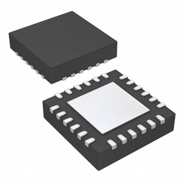


 工商网监
湘ICP备2023018690号
工商网监
湘ICP备2023018690号
