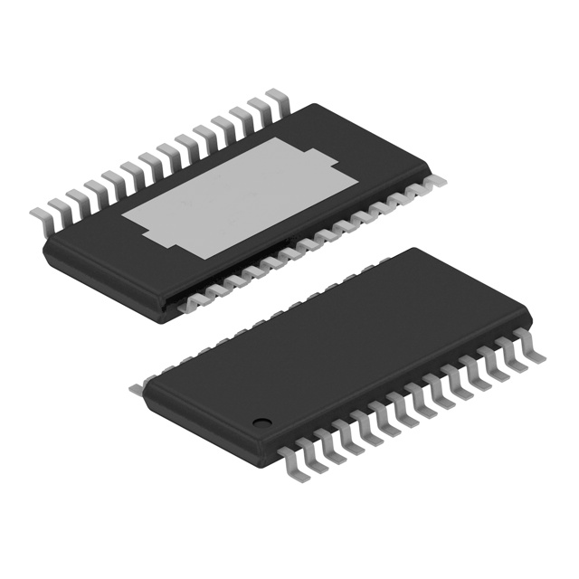
TLC5941
PWP
www.ti.com
RHB
NT
SLVS589D – JULY 2005 – REVISED JANUARY 2008
16-CHANNEL LED DRIVER WITH DOT CORRECTION AND GRAYSCALE PWM CONTROL
FEATURES
APPLICATIONS
• 16 Channels
• 12-Bit (4096 Steps) Grayscale PWM Control
• Dot Correction
– 6 Bit (64 Steps)
• Drive Capability (Constant-Current Sink)
– 0 mA to 80 mA
• LED Power Supply Voltage up to 17 V
• VCC = 3.0 V to 5.5 V
• Serial Data Interface
• Controlled In-Rush Current
• 30-MHz Data Transfer Rate
• CMOS Level I/O
• Error Information
– LOD: LED Open Detection
– TEF: Thermal Error Flag
•
•
•
1
2
VCC
SCLK
GND
Monocolor, Multicolor, Full-Color LED Displays
LED Signboards
Display Back-Lighting
DESCRIPTION
The TLC5941 is a 16-channel, constant-current sink,
LED driver. Each channel has an individually
adjustable 4096-step grayscale PWM brightness
control and a 64-step constant-current sink (dot
correction). The dot correction adjusts the brightness
variations between LED channels and other LED
drivers. Both grayscale control and dot correction are
accessible via a serial interface. A single external
resistor sets the maximum current value of all 16
channels.
The TLC5941 features two error information circuits.
The LED open detection (LOD) indicates a broken or
disconnected LED at an output terminal. The thermal
error flag (TEF) indicates an overtemperature
condition.
SIN
XLAT
CNT
MODE
1 0
IREF
Max. OUTn
Current
V REF
=1.24V
GS Register
MODE
1 0
11
0
GSCLK
BLANK
0
DC Register
0
5
GS Counter
CNT
0
Status
Information:
LOD,
TED,
DC DATA
191
96
12−Bit Grayscale
PWM Control
Constant-Current
Driver
OUT0
Delay
x0
6−Bit Dot Correction
LED Open Detection
Input
Shift
Register
CNT
192
192
GS Register
23
96
95
1 0
96
12
DC Register
11
12−Bit Grayscale
PWM Control
Constant-Current
Driver
OUT1
Delay
x1
6−Bit Dot Correction
6
MODE
LED Open Detection
96
Temperature
Error Flag
(TEF)
LED Open
Detection
(LOD)
CNT
Input
Shift
Register
GS Register
191
XERR
180
DC Register
95
12−Bit Grayscale
PWM Control
Constant-Current
Driver
OUT15
Delay
x15
6−Bit Dot Correction
90
191
LED Open Detection
SOUT
1
2
Please be aware that an important notice concerning availability, standard warranty, and use in critical applications of
Texas Instruments semiconductor products and disclaimers thereto appears at the end of this data sheet.
PowerPAD is a trademark of Texas Instruments.
PRODUCTION DATA information is current as of publication date.
Products conform to specifications per the terms of the Texas
Instruments standard warranty. Production processing does not
necessarily include testing of all parameters.
Copyright © 2005–2008, Texas Instruments Incorporated
�TLC5941
www.ti.com
SLVS589D – JULY 2005 – REVISED JANUARY 2008
These devices have limited built-in ESD protection. The leads should be shorted together or the device placed in conductive foam
during storage or handling to prevent electrostatic damage to the MOS gates.
ORDERING INFORMATION
(1)
TA
PACKAGE (1)
PART NUMBER
–40°C to 85°C
28-pin HTSSOP PowerPAD™
TLC5941PWP
–40°C to 85°C
32-pin 5 mm x 5 mm QFN
TLC5941RHB
–40°C to 85°C
28-pin PDIP
TLC5941NT
For the most current package and ordering information, see the Package Option Addendum at the end
of this document, or see the TI Web site at www.ti.com.
ABSOLUTE MAXIMUM RATINGS.
over operating free-air temperature range (unless otherwise noted) (1)
UNIT
VI
Input voltage range (2)
IO
Output current (dc)
VI
Input voltage range
VO
Output voltage range
ESD rating
VCC
–0.3 V to 6 V
90 mA
V(BLANK), V(SCLK), V(XLAT), V(MODE), V(SIN), V(GSCLK), V(IREF), V(TEST)
–0.3 V to VCC +0.3 V
V(SOUT), V(XERR)
–0.3 V to VCC +0.3 V
V(OUT0) to V(OUT15)
HBM (JEDEC JESD22-A114, Human Body Model)
2 kV
CDM (JEDEC JESD22-C101, Charged Device Model)
500 V
TJ(max) Operating junction temperature
150°C
Tstg
Storage temperature range
TA
Operating ambient temperature range
Package thermal impedance (3)
–55°C to 150°C
–40°C to 85°C
HTSSOP (PWP) (4)
31.58°C/W
QFN (RHB) (4)
35.9°C/W
PDIP (NT)
(1)
(2)
(3)
(4)
2
–0.3 V to 18 V
48°C/W
Stresses beyond those listed under absolute maximum ratings may cause permanent damage to the device. These are stress ratings
only, and functional operation of the device at these or any other conditions beyond those indicated under recommended operating
conditions is not implied. Exposure to absolute maximum rated conditions for extended periods may affect device reliability.
All voltage values are with respect to network ground terminal.
The package thermal impedance is calculated in accordance with JESD 51-7.
With PowerPAD soldered on PCB with 2-oz. trace of copper. See TI application report SLMA002 for further information.
Submit Documentation Feedback
Copyright © 2005–2008, Texas Instruments Incorporated
Product Folder Link(s): TLC5941
�TLC5941
www.ti.com
SLVS589D – JULY 2005 – REVISED JANUARY 2008
RECOMMENDED OPERATING CONDITIONS
PARAMETER
TEST CONDITIONS
MIN
NOM
MAX
UNIT
DC Characteristics
VCC
Supply Voltage
VO
Voltage applied to output (OUT0 - OUT15)
3
VIH
High-level input voltage
VIL
Low-level input voltage
IOH
High-level output current
VCC = 5 V at SOUT
IOL
Low-level output current
VCC = 5 V at SOUT, XERR
IOLC
Constant output current
OUT0 to OUT15
TJ
Operating junction temperature
TA
Operating free-air temperature range
5.5
V
17
V
0.8 VCC
VCC
V
GND
0.2 VCC
V
–1
mA
1
mA
80
mA
–40
125
°C
–40
85
°C
AC Characteristics
VCC = 3 V to 5.5 V, TA = –40°C to 85°C (unless otherwise noted)
f(SCLK)
Data shift clock
frequency
SCLK
30
MHz
f(GSCLK)
Grayscale clock
frequency
GSCLK
30
MHz
twh0/twl0
SCLK pulse duration
SCLK = H/L (See Figure 12)
16
ns
twh1/twl1
GSCLK pulse duration
GSCLK = H/L (See Figure 12)
16
ns
twh2
XLAT pulse duration
XLAT = H (See Figure 12)
20
ns
twh3
BLANK pulse duration
BLANK = H (See Figure 12)
20
ns
tsu0
SIN - SCLK↑ (See Figure 12)
tsu1
SCLK↓ - XLAT↑ (See Figure 12)
10
MODE↑↓ - SCLK↑ (See Figure 12)
10
MODE↑↓ - XLAT↑ (See Figure 12)
10
tsu4
BLANK↓ - GSCLK↑ (See Figure 12)
10
tsu5
XLAT↑ - GSCLK↑ (See Figure 12)
30
th0
SCLK↑ - SIN (See Figure 12)
tsu2
tsu3
Setup time
th1
5
3
XLAT↓ - SCLK↑ (See Figure 12)
10
SCLK↑ - MODE↑↓ (See Figure 12)
10
th3
XLAT↓ - MODE↑↓ (See Figure 12)
10
th4
GSCLK↑ - BLANK↑ (See Figure 12)
10
th2
Hold Time
ns
ns
DISSIPATION RATINGS
PACKAGE
POWER RATING
TA < 25°C
DERATING FACTOR ABOVE TA = 25°C
POWER RATING
TA = 70°C
POWER RATING
TA = 85°C
28-pin HTSSOP with
PowerPAD™
soldered (1)
3958 mW
31.67 mW/°C
2533 mW
2058 mW
28-pin HTSSOP
without PowerPAD™
soldered
2026 mW
16.21 mW/°C
1296 mW
1053 mW
32-pin QFN (1)
3482 mW
27.86 mW/°C
2228 mW
1811 mW
28-pin PDIP
2456 mW
19.65 mW/°C
1572 mW
1277 mW
(1)
The PowerPAD is soldered to the PCB with a 2-oz. copper trace. See application report SLMA002 for further information.
Submit Documentation Feedback
Copyright © 2005–2008, Texas Instruments Incorporated
Product Folder Link(s): TLC5941
3
�TLC5941
www.ti.com
SLVS589D – JULY 2005 – REVISED JANUARY 2008
ELECTRICAL CHARACTERISTICS
VCC = 3 V to 5.5 V, TA = -40°C to 85°C (unless otherwise noted)
PARAMETER
TEST CONDITIONS
VOH
High-level output
voltage
IOH = –1 mA, SOUT
VOL
Low-level output
voltage
IOL = 1 mA, SOUT
II
Input current
MIN
TYP
VCC –0.5
V
0.5
VI = VCC or GND; BLANK, TEST, GSCLK, SCLK, SIN, XLAT pin
–1
VI = GND; MODE pin
–1
Supply current
1
0.9
6
No data transfer, all output OFF, VO = 1 V, R(IREF) = 1.3 kΩ
5.2
12
Data transfer 30 MHz, all output ON, VO = 1 V, R(IREF) = 1.3 kΩ
16
25
Data transfer 30 MHz, all output ON, VO = 1 V, R(IREF) = 640 Ω
30
60
Constant output current All output ON, VO = 1 V, R(IREF) = 640 Ω
Ilkg
Leakage output current
µA
50
No data transfer, all output OFF, VO = 1 V, R(IREF) = 10 kΩ
IO(LC)
V
1
VI = VCC; MODE pin
ICC
MAX UNI
T
54
61
All output OFF, VO = 15 V, R(IREF) = 640 Ω , OUT0 to OUT15
mA
69 mA
0.1
µA
%
All output ON, VO = 1 V, R(IREF) = 640 Ω, OUT0 to OUT15,
–20°C to 85°C (1)
±1
±4
All output ON, VO = 1 V, R(IREF) = 640 Ω, OUT0 to OUT15 (1)
±1
±8
All output ON, VO = 1 V, R(IREF) = 480 Ω, OUT0 to OUT15,
–20°C to 85°C (1)
±1
±6
All output ON, VO = 1 V, R(IREF) = 480 Ω, OUT0 to OUT15 (1)
±1
±8
ΔIO(LC1)
Constant sink current
error
Device to device, averaged current from OUT0 to OUT15,
R(IREF) = 1920 Ω (20 mA) (2)
–2,
0.4
±4
%
ΔIO(LC2)
Constant sink current
error
Device to device, averaged current from OUT0 to OUT15,
R(IREF) = 480 Ω (80 mA) (2)
–2.7,
2
±4
%
±4
Line regulation
All output ON, VO = 1 V, R(IREF) = 640 Ω OUT0 to OUT15,
VCC = 3 V to 5.5 V (3)
±1
ΔIO(LC3)
All output ON, VO = 1 V, R(IREF) = 480 Ω OUT0 to OUT15,
VCC = 3 V to 5.5 V (3)
±1
±6
All output ON, VO = 1 V to 3 V, R(IREF) = 640 Ω, OUT0 to OUT15 (4)
±2
±6
All output ON, VO = 1 V to 3 V, R(IREF) = 480 Ω, OUT0 to OUT15 (4)
±2
±8
%/
V
170
°C
0.3
0.4
V
1.24
1.28
V
ΔIO(LC0)
Constant sink current
error
ΔIO(LC4)
Load regulation
T(TEF)
Thermal error flag
threshold
V(LED)
LED open detection
threshold
V(IREF)
Reference voltage
output
(1)
(2)
(3)
(4)
(5)
4
Junction temperature (5)
RI(REF) = 640 Ω
150
1.20
%
%/
V
The deviation of each output from the average of OUT0-15 constant current. It is calculated by Equation 1 in Table 1.
The deviation of average of OUT1-15 constant current from the ideal constant-current value. It is calculated by Equation 2 in Table 1.
The ideal current is calculated by Equation 3 in Table 1.
The line regulation is calculated by Equation 4 in Table 1.
The load regulation is calculated by Equation 5 in Table 1.
Not tested. Specified by design.
Submit Documentation Feedback
Copyright © 2005–2008, Texas Instruments Incorporated
Product Folder Link(s): TLC5941
�TLC5941
www.ti.com
SLVS589D – JULY 2005 – REVISED JANUARY 2008
Table 1. Test Parameter Equations
D(%) =
D(%) =
I OUTn - I OUTavg _ 0 -15
IOUTavg _ 0 -15
IOUTavg - I OUT (IDEAL )
I OUT (IDEAL )
´ 100
(1)
´ 100
(2)
æ 1.24 V ö
÷÷
IOUT (IDEAL ) = 31.5 ´ çç
è R IREF ø
D(% / V ) =
D(% / V ) =
(3)
(IOUTn at VCC = 5.5 V ) - (I OUTn at VCC = 3.0 V ) 100
´
(I OUTn at VCC = 3.0 V )
2.5
(4)
(IOUTn at VOUTn = 3.0 V ) - (IOUTn at VOUTn = 1.0 V ) 100
´
(IOUTn at VOUTn = 1.0 V )
2 .0
(5)
SWITCHING CHARACTERISTICS
VCC = 3 V to 5.5 V, CL = 15 pF, TA = –40°C to 85°C (unless otherwise noted)
PARAMETER
tr0
tr1
tf0
tf1
Rise time
Fall time
TEST CONDITIONS
MIN
TYP
SOUT
MAX
16
OUTn, VCC = 5 V, TA = 60°C, DCn = 3Fh
10
SOUT
30
16
OUTn, VCC = 5 V, TA = 60°C, DCn = 3Fh
10
30
UNIT
ns
ns
tpd0
SCLK - SOUT (see Figure 12)
30
ns
tpd1
BLANK - OUT0 (see Figure 12)
60
ns
1000
ns
tpd2
Propagation delay time
OUTn - XERR (see Figure 12)
tpd3
GSCLK - OUT0 (see Figure 12)
tpd4
XLAT - IOUT (dot correction) (see Figure 12)
td
Output delay time
OUTn - OUT(n+1) (see Figure 12)
ton_err
Output on-time error
touton – Tgsclk (see Figure 12), GSn = 01h,
GSCLK = 11 MHz
10
60
ns
1000
ns
20
30
ns
–50
–90
ns
Submit Documentation Feedback
Copyright © 2005–2008, Texas Instruments Incorporated
Product Folder Link(s): TLC5941
5
�TLC5941
www.ti.com
SLVS589D – JULY 2005 – REVISED JANUARY 2008
DEVICE INFORMATION
PWP PACKAGE
(TOP VIEW)
GND
BLANK
XLAT
SCLK
SIN
MODE
OUT0
OUT1
OUT2
OUT3
OUT4
OUT5
OUT6
OUT7
1
2
3
4
5
6
7
8
9
10
11
12
13
14
Thermal
PAD
NT PACKAGE
(TOP VIEW)
28
27
26
25
24
23
22
21
20
19
18
17
16
15
VCC
IREF
TEST
GSCLK
SOUT
XERR
OUT15
OUT14
OUT13
OUT12
OUT11
OUT10
OUT9
OUT8
OUT1
1
28
OUT0
OUT2
2
27
MODE
OUT3
3
26
SIN
OUT4
4
25
SCLK
OUT5
5
24
XLAT
OUT6
6
23
BLANK
OUT7
7
22
GND
OUT8
8
21
VCC
OUT9
9
20
IREF
OUT10
10
19
TEST
OUT11
11
18
GSCLK
OUT12
12
17
SOUT
OUT13
13
16
XERR
OUT14
14
15
OUT15
OUT13
OUT12
OUT11
19
18
17
OUT15
OUT14
21
20
SOUT
XERR
23
22
GSCLK
24
RHB PACKAGE
(TOP VIEW)
TEST
25
16
OUT10
IREF
26
15
OUT9
VCC
27
14
OUT8
13
NC
NC
28
THERMAL
PAD
OUT6
9
OUT5
OUT4 8
10
32
OUT3 7
31
XLAT
OUT2 6
BLANK
OUT1 5
OUT7
OUT0 4
NC
11
SIN 2
12
30
MODE 3
29
SCLK 1
NC
GND
NC − No internal connection
6
Submit Documentation Feedback
Copyright © 2005–2008, Texas Instruments Incorporated
Product Folder Link(s): TLC5941
�TLC5941
www.ti.com
SLVS589D – JULY 2005 – REVISED JANUARY 2008
TERMINAL FUNCTION
TERMINAL
NT
PWP
RHB
NAME
NO.
NO.
NO.
I/O
DESCRIPTION
BLANK
23
2
31
I
Blank all outputs. When BLANK = H, all OUTn outputs are forced OFF.
GS counter is also reset. When BLANK = L, OUTn are controlled by
grayscale PWM control.
GND
22
GSCLK
18
1
30
G
Ground
25
24
I
Reference clock for grayscale PWM control
IREF
20
-
27
26
I/O
-
12, 13, 28, 29
OUT0
28
7
4
O
Constant-current output
OUT1
1
8
5
O
Constant-current output
OUT2
2
9
6
O
Constant-current output
OUT3
3
10
7
O
Constant-current output
OUT4
4
11
8
O
Constant-current output
OUT5
5
12
9
O
Constant-current output
OUT6
6
13
10
O
Constant-current output
OUT7
7
14
11
O
Constant-current output
OUT8
8
15
14
O
Constant-current output
OUT9
9
16
15
O
Constant-current output
OUT10
10
17
16
O
Constant-current output
OUT11
11
18
17
O
Constant-current output
OUT12
12
19
18
O
Constant-current output
OUT13
13
20
19
O
Constant-current output
OUT14
14
21
20
O
Constant-current output
OUT15
15
22
21
O
Constant-current output
SCLK
25
4
1
I
Serial data shift clock
SIN
26
5
2
I
Serial data input
SOUT
17
24
23
O
Serial data output
TEST
19
26
25
I
Test pin: TEST must be connected to VCC.
VCC
21
28
27
I
Power supply voltage.
MODE
27
6
3
I
Input mode-change pin. When MODE = GND, the device is in GS
mode. When MODE = VCC, the device is in DC mode.
XERR
16
23
22
O
Error output. XERR is an open-drain terminal. XERR goes L when
LOD or TEF is detected.
XLAT
24
3
32
I
Level triggered latch signal. When XLAT = high, the TLC5941 writes
data from the input shift register to either GS register (MODE = low) or
DC register (MODE = high). When XLAT=low, the data in the GS or
DC registers is held constant and does not change.
NC
Reference current terminal
No connection
Submit Documentation Feedback
Copyright © 2005–2008, Texas Instruments Incorporated
Product Folder Link(s): TLC5941
7
�TLC5941
www.ti.com
SLVS589D – JULY 2005 – REVISED JANUARY 2008
PARAMETER MEASUREMENT INFORMATION
PIN EQUIVALENT INPUT AND OUTPUT SCHEMATIC DIAGRAMS
Resistor values are equivalent resistance and not tested.
INPUT EQUIVALENT CIRCUIT
(BLANK, XLAT, SCLK, SIN, GSCLK, TEST)
OUTPUT EQUIVALENT CIRCUIT (SOUT)
VCC
23 �
400 �
INPUT
SOUT
23 �
GND
GND
INPUT EQUIVALENT CIRCUIT (IREF)
OUTPUT EQUIVALENT CIRCUIT (XERR)
VCC
_
400 �
INPUT
23 �
Amp
XERR
+
100 �
GND
GND
INPUT EQUIVALENT CIRCUIT (VCC)
OUTPUT EQUIVALENT CIRCUIT (OUT)
OUT
INPUT
GND
GND
INPUT EQUIVALENT CIRCUIT (MODE)
INPUT
GND
Figure 1. Input and Output Equivalent Circuits
8
Submit Documentation Feedback
Copyright © 2005–2008, Texas Instruments Incorporated
Product Folder Link(s): TLC5941
�TLC5941
www.ti.com
SLVS589D – JULY 2005 – REVISED JANUARY 2008
PARAMETER MEASUREMENT INFORMATION (continued)
t who , t wIO, twh1, twl1, tsu0
t su4, th4
V(LED) = 4 V
SOUT
Test Point
RL = 51
CL = 15 pF
OUTn
Test Point
CL = 15 pF
IOLC, IOLC3, IOLC4
V(LED) = 1 V
OUT0
VCC = 0 V ~ 7 V
OUTn
+ _
OUT15
IREF
Test Point
RIREF = 640
Figure 2. Parameter Measurement Circuits
Submit Documentation Feedback
Copyright © 2005–2008, Texas Instruments Incorporated
Product Folder Link(s): TLC5941
9
�TLC5941
www.ti.com
SLVS589D – JULY 2005 – REVISED JANUARY 2008
Typical Characteristics
REFERENCE RESISTOR
vs
OUTPUT CURRENT
POWER DISSIPATION RATE
vs
FREE-AIR TEMPERATURE
4000
10 k
R(IREF) − Reference Resistor − W
TLC5941PWP+
Power Dissipation Rate − mW
3.84 k
1.92 k
1.28 k
1k
0.96 k
0.79 k
0.64 k
0.55 k
0.48 k
100
0
10
90
70
TLC5941NT
2000
TLC5941PWP−
1000
0
−40
80
0
20
40
60
80
TA − Free-Air Temperature − 5C
Figure 4.
OUTPUT CURRENT
vs
OUTPUT VOLTAGE
OUTPUT CURRENT
vs
OUTPUT VOLTAGE
65
IO = 80 mA
IO = 60 mA,
VCC = 3.3 V
64
IO - Output Current - mA
IO = 60 mA
60
50
IO = 40 mA
40
30
20
TA = 25°C
TA = 85°C
63
70
IO = 20 mA
62
61
60
TA = -40°C
59
58
57
IO = 5 mA
10
56
0
55
0
0.5
1
1.5
2
VO - Output Voltage - V
2.5
3
0
0.5
1
1.5
2
2.5
3
VO - Output Voltage - V
Figure 5.
10
−20
Figure 3.
TA = 25°C,
VCC = 3.3 V
80
IO - Output Current - mA
20
30
40
50
60
IO(LC) − Output Current − mA
TLC5941RHB
3000
Figure 6.
Submit Documentation Feedback
Copyright © 2005–2008, Texas Instruments Incorporated
Product Folder Link(s): TLC5941
�TLC5941
www.ti.com
SLVS589D – JULY 2005 – REVISED JANUARY 2008
Typical Characteristics (continued)
DELTA OUTPUT CURRENT
vs
FREE-AIR TEMPERATURE
DELTA OUTPUT CURRENT
vs
OUTPUT CURRENT
8
8
IO = 60 mA
6
6
4
4
VCC = 5 V
VCC = 3.3 V
2
Max
2
ΔIOLC - %
ΔIOLC - %
TA = 25°C,
VCC = 3.3 V
0
0
-2
-2
-4
-4
-6
-6
-8
-40
-20
0
20
40
60
80
TA - Ambient Temperature - °C
Min
-8
0
100
20
40
60
IO - Output Current - mA
Figure 7.
Figure 8.
DOT CORRECTION LINEARITY (ABS Value)
DOT CORRECTION LINEARITY (ABS Value)
70
90
TA = 25°C,
VCC = 3.3 V
80
70
IO = 60 mA,
VCC = 3.3 V
IO = 80 mA
60
IO = 60 mA
IO - Output Current - mA
IO - Output Current - mA
80
60
50
40
IO = 30 mA
30
TA = 85°C
50
TA = 25°C
40
30
TA = -40°C
20
20
IO = 5 mA
10
10
0
0
0
10
20
30
40
50
Dot Correction Data - dec
Figure 9.
60
70
0
10
20
30
40
50
Dot Correction Data - dec
60
70
Figure 10.
Submit Documentation Feedback
Copyright © 2005–2008, Texas Instruments Incorporated
Product Folder Link(s): TLC5941
11
�TLC5941
www.ti.com
SLVS589D – JULY 2005 – REVISED JANUARY 2008
Typical Characteristics (continued)
DOT CORRECTION LINEARITY (ABS Value)
70
60
TA = 25°C,
IO = 60 mA
IO - Output Current - mA
VCC = 3.3 V
50
40
30
VCC = 5 V
20
10
0
0
12
10
20
30
40
50
Dot Correction Data - dec
Figure 11.
Submit Documentation Feedback
60
70
Copyright © 2005–2008, Texas Instruments Incorporated
Product Folder Link(s): TLC5941
�TLC5941
www.ti.com
SLVS589D – JULY 2005 – REVISED JANUARY 2008
PRINCIPLES OF OPERATION
SERIAL INTERFACE
The TLC5941 has a flexible serial interface, which can be connected to microcontrollers or digital signal
processors in various ways. Only 3 pins are needed to input data into the device. The rising edge of SCLK signal
shifts the data from the SIN pin to the internal register. After all data is clocked in, a high-level pulse of XLAT
signal latches the serial data to the internal registers. The internal registers are level-triggered latches of XLAT
signal. All data are clocked in with the MSB first. The length of serial data is 96 bit or 192 bit, depending on the
programming mode. Grayscale data and dot correction data can be entered during a grayscale cycle. Although
new grayscale data can be clocked in during a grayscale cycle, the XLAT signal should only latch the grayscale
data at the end of the grayscale cycle. Latching in new grayscale data immediately overwrites the existing
grayscale data. Figure 12 shows the timing chart. More than two TLC5941s can be connected in series by
connecting an SOUT pin from one device to the SIN pin of the next device. An example of cascading two
TLC5941s is shown in Figure 13. The SOUT pin can also be connected to the controller to receive status
information from TLC5941 as shown in Figure 22.
MODE
DC Data Input Mode
GS Data Input Mode
th3
tsu3
twh2
XLAT
1st GS Data Input Cycle
SIN
DC
MSB
SCLK
GS1
LSB
tsu2
th2
GS2
MSB
GS2
LSB
th1
tsu1
1
96
1
2nd GS Data Input Cycle
GS1
MSB
DC
LSB
GS3
MSB
tsu0
twh0
192
193
th0
193
192
1
tpd0
twl0
-
SOUT
DC
MSB
-
GS1
MSB
-
1
SID1 SID1
MSB MSB-1
SID2 SID2
MSB MSB-1
SID1 GS2
LSB MSB
twh3
BLANK
1st GS Data Output Cycle
tsu5
GSCLK
2nd GS Data Output Cycle
1
tpd4
4096
1
tpd3
tpd1
td
tpd1 + td
twl1
Tgsclk
tpd3
OUT0
(current)
twh1
tsu4
th4
tpd3 + td
touton
OUT1
(current)
15 x td
tpd1 + 15 x td
OUT15
(current)
tpd2
XERR
Figure 12. Serial Data Input Timing Chart
SIN(a)
SIN
SOUT
TLC5941 (a)
SIN
SOUT
SOUT(b )
TLC5941 (b)
SCLK, XLAT,
BLANK,
GSCLK,
MODE
Figure 13. Cascading Two TLC5941 Devices
Submit Documentation Feedback
Copyright © 2005–2008, Texas Instruments Incorporated
Product Folder Link(s): TLC5941
13
�TLC5941
www.ti.com
SLVS589D – JULY 2005 – REVISED JANUARY 2008
MODE
XLAT
SIN(a)
SCLK
DCb
MSB
DCa
LSB
GSb1
MSB
1
192
1
384
96X2
-
SOUT(b)
GSb2
MSB
GSa1
LSB
385
GSa2
LSB
GSb3
MSB
385
384
1
1
192X2
DCb
MSB
-
SIDb1 SIDb1
MSB MSB-1
GSb1
MSB
-
SIDa1
LSB
SIDb2 SIDb2
MSB MSB-1
GSb2
MSB
BLANK
1
GSCLK
1
4096
OUT0
(current)
OUT1
(current)
OUT15
(current)
XERR
Figure 14. Timing Chart for Two Cascaded TLC5941 Devices
ERROR INFORMATION OUTPUT
The open-drain output XERR is used to report both of the TLC5941 error flags, TEF and LOD. During normal
operating conditions, the internal transistor connected to the XERR pin is turned off. The voltage on XERR is
pulled up to VCC through an external pullup resistor. If TEF or LOD is detected, the internal transistor is turned
on, and XERR is pulled to GND. Because XERR is an open-drain output, multiple ICs can be ORed together and
pulled up to VCC with a single pullup resistor. This reduces the number of signals needed to report a system error
(see Figure 22).
To differentiate LOD and TEF signal from XERR pin, LOD can be masked out with BLANK = HIGH.
Table 2. XERR Truth Table
ERROR CONDITION
ERROR INFORMATION
TEMPERATURE
OUTn VOLTAGE
TEF
LOD
TJ < T(TEF)
Don't Care
L
X
TJ > T(TEF)
Don't Care
H
X
OUTn > V(LED)
L
L
OUTn < V(LED)
L
H
OUTn > V(LED)
H
L
OUTn < V(LED)
H
H
TJ < T(TEF)
TJ > T(TEF)
SIGNALS
BLANK
H
XERR
H
L
H
L
L
L
L
TEF: THERMAL ERROR FLAG
The TLC5941 provides a temperature error flag (TEF) circuit to indicate an overtemperature condition of the IC. If
the junction temperature exceeds the threshold temperature (160C typical), TEF becomes H and XERR pin goes
to low level. When the junction temperature becomes lower than the threshold temperature, TEF becomes L and
XERR pin becomes high impedance. TEF status can also be read out from the TLC5941 status register.
14
Submit Documentation Feedback
Copyright © 2005–2008, Texas Instruments Incorporated
Product Folder Link(s): TLC5941
�TLC5941
www.ti.com
SLVS589D – JULY 2005 – REVISED JANUARY 2008
LOD: LED OPEN DETECTION
The TLC5941 has an LED-open detection circuit that detects broken or disconnected LED's. The LED open
detector pulls the XERR pin to GND when an open LED is detected. XERR and the corresponding error bit in the
Status Information Data is only active under the following open LED conditions.
1. OUTn is on and the time tpd2 (1 µs typical) has passed.
2. The voltage of OUTn is < 0.3V (typical)
The LOD status of each output can be also read out from the SOUT pin. See the STATUS INFORMATION
OUTPUT section for details. The LOD error bits are latched into the Status Information Data when XLAT returns
to a low after a high. Therefore, the XLAT pin must be pulsed high then low while XERR is active in order to latch
the LOD error into the Status Information Data for subsequent reading via the serial shift register.
DELAY BETWEEN OUTPUTS
The TLC5941 has graduated delay circuits between outputs. These circuits can be found in the constant current
driver block of the device (see the functional block diagram). The fixed-delay time is 20ns (typical), OUT0 has no
delay, OUT1 has 20ns delay, and OUT2 has 40ns delay, etc. The maximum delay is 300ns from OUT0 to
OUT15. The delay works during switch on and switch off of each output channel. These delays prevent large
inrush currents which reduces the bypass capacitors when the outputs turn on.
OUTPUT ENABLE
All OUTn channels of the TLC5941 can be switched off with one signal. When BLANK is set high, all OUTn
channels are disabled, regardless of logic operations of the device. The grayscale counter is also reset. When
BLANK is set low, all OUTn channels work under normal conditions. If BLANK goes low and then back high
again in less than 300ns, all outputs programmed to turn on still turn on for either the programmed number of
grayscale clocks, or the length of time that the BLANK signal was low, which ever is lower. For example, if all
outputs are programmed to turn on for 1ms, but the BLANK signal is only low for 200ns, all outputs still turn on
for 200ns, even though some outputs are turning on after the BLANK signal has already gone high.
Table 3. BLANK Signal Truth Table
BLANK
OUT0 - OUT15
LOW
Normal condition
HIGH
Disabled
Submit Documentation Feedback
Copyright © 2005–2008, Texas Instruments Incorporated
Product Folder Link(s): TLC5941
15
�TLC5941
www.ti.com
SLVS589D – JULY 2005 – REVISED JANUARY 2008
SETTING MAXIMUM CHANNEL CURRENT
The maximum output current per channel is programmed by a single resistor, R(IREF), which is placed between
IREF pin and GND pin. The voltage on IREF is set by an internal band gap V(IREF) with a typical value of
1.24 V. The maximum channel current is equivalent to the current flowing through R(IREF) multiplied by a factor of
31.5. The maximum output current can be calculated by Equation 6:
V
(IREF)
I max +
31.5
R
(IREF)
(6)
where:
V(IREF) = 1.24 V
R(IREF) = User-selected external resistor.
Imax must be set between 5 mA and 80 mA. The output current may be unstable if Imax is set lower than 5 mA.
Output currents lower than 5 mA can be achieved by setting Imax to 5 mA or higher and then using dot
correction.
Figure 3 shows the maximum output current IO versus R(IREF). R(IREF) is the value of the resistor between IREF
terminal to GND, and IO is the constant output current of OUT0 to OUT15. A variable power supply may be
connected to the IREF pin through a resistor to change the maximum output current per channel. The maximum
output current per channel is 31.5 times the current flowing out of the IREF pin.
POWER DISSIPATION CALCULATION
The device power dissipation needs to be below the power dissipation rate of the device package to ensure
correct operation. Equation 7 calculates the power dissipation of device:
P
D
ǒ
+ V
CC
I
Ǔ ) ǒVOUT
CC
I
MAX
N
DCn
63
d
PWM
Ǔ
(7)
where:
VCC: device supply voltage
ICC: device supply current
VOUT: TLC5941 OUTn voltage when driving LED current
IMAX: LED current adjusted by R(IREF) Resistor
DCn: maximum dot correction value for OUTn
N: number of OUTn driving LED at the same time
dPWM: duty cycle defined by BLANK pin or GS PWM value
OPERATING MODES
The TLC5941 has two operating modes defined by MODE as shown in Table 4. The GS and DC registers are
set to random values that are not known just after power on. The GS and DC values must be programmed
before turning on the outputs. Please note that when initially setting GS and DC data after power on, the GS data
must be set before the DC data is set. Failure to set GS data before DC data may result in the first bit of GS data
being lost. XLAT must be low when the MODE pin goes high-to-low or low-to-high to change back and forth
between GS mode and DC mode.
Table 4. TLC5941 Operating Modes Truth Table
16
MODE
INPUT SHIFT REGISTER
OPERATING MODE
GND
192 bit
Grayscale PWM Mode
VCC
96 bit
Dot Correction Data Input Mode
Submit Documentation Feedback
Copyright © 2005–2008, Texas Instruments Incorporated
Product Folder Link(s): TLC5941
�TLC5941
www.ti.com
SLVS589D – JULY 2005 – REVISED JANUARY 2008
SETTING DOT CORRECTION
The TLC5941 has the capability to fine-adjust the output current of each channel (OUT0 to OUT15)
independently. This is also called dot correction. This feature is used to adjust the brightness deviations of LEDs
connected to the output channels OUT0 to OUT15. Each of the 16 channels can be programmed with a 6-bit
word. The channel output can be adjusted in 64 steps from 0% to 100% of the maximum output current Imax. The
TEST pin must be connected to VCC to ensure proper operation of the dot correction circuitry. Equation 8
determines the output current for each output n:
I
+ I max DCn
OUTn
63
(8)
where:
Imax = the maximum programmable output current for each output.
DCn = the programmed dot correction value for output n (DCn = 0 to 63).
n = 0 to 15
Figure 15 shows the dot correction data packet format which consists of 6 bits x 16 channel, total 96 bits. The
format is Big-Endian format. This means that the MSB is transmitted first, followed by the MSB-1, etc. The DC
15.5 in Figure 15 stands for the 5th-most significant bit for output 15.
MSB
LSB
0
5
6
89
90
95
DC 15.5
DC 15.0
DC 14.5
DC 1.0
DC 0.5
DC 0.0
DC OUT15
DC OUT0
DC OUT14 − DC OUT1
Figure 15. Dot Correction Data Packet Format
When MODE is set to VCC, the TLC5941 enters the dot correction data input mode. The length of input shift
register becomes 96bits. After all serial data are shifted in, the TLC5941 writes the data in the input shift register
to DC register when XLAT is high, and holds the data in the DC register when XLAT is low. The DC register is a
level triggered latch of XLAT signal. Since XLAT is a level-triggered signal, SCLK and SIN must not be changed
while XLAT is high. After XLAT goes low, data in the DC register is latched and does not change. BLANK signal
does not need to be high to latch in new data. When XLAT goes high, the new dot-correction data immediately
becomes valid and changes the output currents if BLANK is low. XLAT has setup time (tsu1) and hold time (th1)
to SCLK as shown in Figure 12.
Submit Documentation Feedback
Copyright © 2005–2008, Texas Instruments Incorporated
Product Folder Link(s): TLC5941
17
�TLC5941
www.ti.com
SLVS589D – JULY 2005 – REVISED JANUARY 2008
To input data into the dot correction register, MODE must be set to VCC. The internal input shift register is then
set to 96-bit width. After all serial data are clocked in, a rising edge of XLAT is used to latch the data into the dot
correction register. Figure 16 shows the dc data input timing chart.
DC Mode Data
Input Cycle n
DC Mode Data
Input Cycle n+1
VCC
MODE
SIN
DC n−1
LSB
DC n
MSB
DC n
MSB−1
DC n
MSB−2
DC n
LSB+1
DC n
LSB
DC n+1
MSB
DC n+1
MSB−1
twh0
SCLK
1
2
3
95
96
1
2
twl0
SOUT
DC n−1
MSB
DC n−1
MSB−1
DC n−1
MSB−2
DC n−1
LSB+1
DC n−1
LSB
tsu1
DC n
MSB
DC n
MSB−1
DC n
MSB−2
twh2
th1
XLAT
Figure 16. Dot Correction Data Input Timing Chart
18
Submit Documentation Feedback
Copyright © 2005–2008, Texas Instruments Incorporated
Product Folder Link(s): TLC5941
�TLC5941
www.ti.com
SLVS589D – JULY 2005 – REVISED JANUARY 2008
SETTING GRAYSCALE
The TLC5941 can adjust the brightness of each channel OUTn using a PWM control scheme. The use of 12 bits
per channel results in 4096 different brightness steps, from 0% to 100% brightness. Equation 9 determines the
brightness level for each output n:
Brightness in % + GSn
100
4095
(9)
where:
GSn = the programmed grayscale value for output n (GSn = 0 to 4095)
n = 0 to 15
Grayscale data for all OUTn
The input shift register enters grayscale data into the grayscale register for all channels simultaneously. The
complete grayscale data format consists of 16 x 12 bit words, which forms a 192-bit wide data packet (see
Figure 17). The data packet must be clocked in with the MSB first.
MSB
0
11
12
179
180
LSB
191
GS 15.11
GS 15.0
GS 14.11
GS 1.0
GS 0.11
GS 0.0
GS OUT15
GS OUT14 − GS OUT1
GS OUT0
Figure 17. Grayscale Data Packet Format
When MODE is set to GND, the TLC5941 enters the grayscale data input mode. The device switches the input
shift register to 192-bit width. After all data is clocked in, a rising edge of the XLAT signal latches the data into
the grayscale register (see Figure 18). New grayscale data immediately becomes valid at the rising edge of the
XLAT signal; therefore, new grayscale data should be latched at the end of a grayscale cycle when BLANK is
high. The first GS data input cycle after dot correction requires an additional SCLK pulse after the XLAT signal to
complete the grayscale update cycle. All GS data in the input shift register is replaced with status information
data (SID) after updating the grayscale register.
First GS Mode Data
Input Cycle After DC Data Input Cycle
DC Mode Data
Input Cycle
Following GS Mode Data
Input Cycle
MODE
t h3
t h3
t su3
XLAT
t wh2
SIN
GS
MSB
DC
LSB
GS n + 1
LSB
t h1
t h2
SCLK
GS + 1
MSB
GS
LSB
t su1
t su2
96
192
1
193
1
192
t pd0
n
SOUT DC
LSB
DC
MSB
X
X
GS
MSB
SID
MSB
SID
MSB−1
SID
LSB
SID n + 1
MSB
Figure 18. Grayscale Data Input Timing Chart
Submit Documentation Feedback
Copyright © 2005–2008, Texas Instruments Incorporated
Product Folder Link(s): TLC5941
19
�TLC5941
www.ti.com
SLVS589D – JULY 2005 – REVISED JANUARY 2008
STATUS INFORMATION OUTPUT
The TLC5941 does have a status information register, which can be accessed in grayscale mode (MODE =
GND). After the XLAT signal latches the data into the GS register, the input shift register data is replaced with
status information data (SID) of the device (see Figure 18). LOD, TEF, and dot-correction register data can be
read out at the SOUT pin. The status information data packet is 192 bits wide. Bits 0 – 15 contain the LOD status
of each channel. Bit 16 contains the TEF status. Bits 24 – 119 contain the data of the dot-correction register. The
remaining bits are reserved. The complete status information data packet is shown in Figure 19.
SOUT outputs the MSB of the SID at the same time the SID are stored in the SID register, as shown in
Figure 20. The next SCLK pulse, which will be the clock for receiving the MSB of the next grayscale data,
transmits MSB-1 of SID. If output voltage is < 0.3 V (typical) when the output sink current turns on, LOD status
flag becomes active. The LOD status flag is an internal signal which pulls XERR pin down to low when the LOD
status flag becomes active. The delay time, tpd2 (1 µs maximum), is from the time of turning on the output sink
current to the time LOD status flag becomes valid. The timing for each channels LOD status to become valid is
shifted by the 30-ns (maximum), channel-to-channel turn-on time. After the first GSCLK goes high, OUT0 LOD
status is valid; tpd3 + tpd2 = 60 nS + 1 µs = 1.06 µs. OUT1 LOD status is valid; tpd3 + td + tpd2 = 60 ns + 30 ns
+ 1 µs = 1.09 µs. OUT2 LOD status is valid; tpd3 + 2*td + tpd2 = 1.12 µs, and so on. It takes 1.51µs maximum
(tpd3 + 15*td + tpd2) from the first GSCLK rising edge until all LOD become valid; tsuLOD must be > 1.51 µs
(see Figure 20) to ensure that all LOD data are valid.
MSB
LSB
0
15
16
LOD 15
LOD 0
TEF
LOD Data
23
X
X
TEF
24
DC 15.5
119
120
191
DC 0.0
X
X
DC Values
Reserved
Figure 19. Status Information Data Packet Format
20
Submit Documentation Feedback
Copyright © 2005–2008, Texas Instruments Incorporated
Product Folder Link(s): TLC5941
�TLC5941
www.ti.com
SLVS589D – JULY 2005 – REVISED JANUARY 2008
MODE
GS Data Input Mode
tsuLOD > tpd3 + td ´ 15 + tpd2
tsuLOD
XLAT
1st GS Data Input Cycle
2nd GS Data Input Cycle
SIN
GS1
MSB
GS1
LSB
SCLK
1
192
SOUT
-
-
GS2
MSB
193
GS1
MSB
GS2
LSB
192
1
SID1
MSB
SID1
MSB-1
SID1
LSB
GS2
MSB
(1st GS Data Output Cycle)
BLANK
GSCLK
4096
1
tpd3
OUT0
(current)
td
OUT1
(current)
15 x td
OUT15
(current)
tpd2
XERR
tpd3 + 15 x td + tpd2
Figure 20. Readout Status Information Data (SID) Timing Chart
The LOD status of each output can be read out from the SOUT pin. The LOD error bits are latched into the
Status Information Data when XLAT returns to a low after a high. Therefore, the XLAT pin must be pulsed high
then low while XERR is active in order to latch the LOD error into the Status Information Data for subsequent
reading via the serial shift register.
Submit Documentation Feedback
Copyright © 2005–2008, Texas Instruments Incorporated
Product Folder Link(s): TLC5941
21
�TLC5941
www.ti.com
SLVS589D – JULY 2005 – REVISED JANUARY 2008
GRAYSCALE PWM OPERATION
The grayscale PWM cycle starts with the falling edge of BLANK. The first GSCLK pulse after BLANK goes low
increases the grayscale counter by one and switches on all OUTn with grayscale value not zero. Each following
rising edge of GSCLK increases the grayscale counter by one. The TLC5941 compares the grayscale value of
each output OUTn with the grayscale counter value. All OUTn with grayscale values equal to the counter values
are switched off. A BLANK=H signal after 4096 GSCLK pulses resets the grayscale counter to zero and
completes the grayscale PWM cycle (see Figure 21). When the counter reaches a count of FFFh, the counter
stops counting and all outputs turn off. Pulling BLANK high before the counter reaches FFFh immediately resets
the counter to zero.
GS PWM
Cycle n
BLANK
t wl1
t wh1
t h4
GSCLK
1
OUT0
(Current)
OUT1
(Current)
t pd1
t pd1 + td
GS PWM
Cycle n+1
2
t pd3
4096
3
t wl1
t wh3
t su4
1
t pd3
nxt d
t pd3+ n x t d
t pd1 + 15 x td
OUT15
(Current)
t pd2
XERR
Figure 21. Grayscale PWM Cycle Timing Chart
Output On Time
The amount of time that each output is turned on is a function of the grayscale clock frequency and the
programmed grayscale PWM value. The on-time of each output can be calculated using Equation 10.
GSn
T _ on n =
+ t on _ err
f( GSCLK )
(10)
Where
• T_onn is the time that OUTn turns on and sinks current
• GSn is OUTn's programmed grayscale PWM value between 0 and 4095
• ton_err is the Output on time error defined in the Switching Characteristics Table
When using Equation 10 with very high GSCLK frequencies and very low grayscale PWM values, the resulting
T_on time may be negative. If T_on is negative, the output does not turn on. For example, using f(GSCLK) = 30
MHz, GSn = 1, and the typical ton_err = 50 nS, Equation 10 calculates that OUTn turns on for –16.6 nS. This
output may not turn on under these conditions. Increasing the PWM value or reducing the GSCLK clock
frequency ensures turn-on.
22
Submit Documentation Feedback
Copyright © 2005–2008, Texas Instruments Incorporated
Product Folder Link(s): TLC5941
�TLC5941
www.ti.com
SLVS589D – JULY 2005 – REVISED JANUARY 2008
SERIAL DATA TRANSFER RATE
Figure 22 shows a cascading connection of n TLC5941 devices connected to a controller, building a basic
module of an LED display system. There is no TLC5941 limitation to the maximum number of ICs that can be
cascaded. The maximum number of cascading TLC5941 devices depends on the application system and is in
the range of 40 devices. Equation 11 calculates the minimum frequency needed:
f
+ 4096
f
(GSCLK)
(update)
f
(SCLK)
+ 193
f
(update)
n
(11)
where:
f(GSCLK): minimum frequency needed for GSCLK
f(SCLK): minimum frequency needed for SCLK and SIN
f(update): update rate of whole cascading system
n: number cascaded of TLC5941 device
Application Example
VCC
V(LED)
V(LED)
V(LED)
V(LED)
100 k
OUT0
XERR
SCLK
SCLK
BLANK
100 nF
SOUT
VCC
GSCLK
IREF
BLANK
IC 0
TLC5941
MODE
VCC
TEST
100 nF
XLAT
TLC5941
MODE
VCC
SOUT
XERR
SCLK
XLAT
MODE
OUT15
SIN
VCC
GSCLK
GSCLK
OUT0
SOUT
XERR
XLAT
Controller
OUT15
SIN
SIN
IREF
BLANK
TEST
IC n
6
Figure 22. Cascading Devices
Submit Documentation Feedback
Copyright © 2005–2008, Texas Instruments Incorporated
Product Folder Link(s): TLC5941
23
�PACKAGE OPTION ADDENDUM
www.ti.com
14-Oct-2022
PACKAGING INFORMATION
Orderable Device
Status
(1)
Package Type Package Pins Package
Drawing
Qty
Eco Plan
(2)
Lead finish/
Ball material
MSL Peak Temp
Op Temp (°C)
Device Marking
(3)
Samples
(4/5)
(6)
TLC5941PWP
ACTIVE
HTSSOP
PWP
28
50
RoHS & Green
NIPDAU
Level-2-260C-1 YEAR
-40 to 85
TLC5941
Samples
TLC5941PWPG4
ACTIVE
HTSSOP
PWP
28
50
RoHS & Green
NIPDAU
Level-2-260C-1 YEAR
-40 to 85
TLC5941
Samples
TLC5941PWPR
ACTIVE
HTSSOP
PWP
28
2000
RoHS & Green
NIPDAU
Level-2-260C-1 YEAR
TLC5941
Samples
TLC5941RHBR
ACTIVE
VQFN
RHB
32
3000
RoHS & Green
Call TI | NIPDAU
Level-2-260C-1 YEAR
TLC
5941
Samples
TLC5941RHBT
ACTIVE
VQFN
RHB
32
250
RoHS & Green
NIPDAU
Level-2-260C-1 YEAR
-40 to 85
TLC
5941
Samples
TLC5941RHBTG4
ACTIVE
VQFN
RHB
32
250
RoHS & Green
NIPDAU
Level-2-260C-1 YEAR
-40 to 85
TLC
5941
Samples
(1)
The marketing status values are defined as follows:
ACTIVE: Product device recommended for new designs.
LIFEBUY: TI has announced that the device will be discontinued, and a lifetime-buy period is in effect.
NRND: Not recommended for new designs. Device is in production to support existing customers, but TI does not recommend using this part in a new design.
PREVIEW: Device has been announced but is not in production. Samples may or may not be available.
OBSOLETE: TI has discontinued the production of the device.
(2)
RoHS: TI defines "RoHS" to mean semiconductor products that are compliant with the current EU RoHS requirements for all 10 RoHS substances, including the requirement that RoHS substance
do not exceed 0.1% by weight in homogeneous materials. Where designed to be soldered at high temperatures, "RoHS" products are suitable for use in specified lead-free processes. TI may
reference these types of products as "Pb-Free".
RoHS Exempt: TI defines "RoHS Exempt" to mean products that contain lead but are compliant with EU RoHS pursuant to a specific EU RoHS exemption.
Green: TI defines "Green" to mean the content of Chlorine (Cl) and Bromine (Br) based flame retardants meet JS709B low halogen requirements of


 工商网监
湘ICP备2023018690号
工商网监
湘ICP备2023018690号
