TLK4201EA
www.ti.com
SLLS719 – APRIL 2006
4.25-GBPS CABLE AND PC BOARD EQUALIZER
FEATURES
APPLICATIONS
•
•
•
•
•
•
•
•
•
•
•
•
•
•
•
Multirate Operation up to 4.25 Gbps
Compensates up to 12 dB Loss at 2.1 GHz
Suitable to Receive 4.25 Gbps Data Over up
to 36 Inches (0.91 Meters) of FR4 PC Boards
Suitable to Receive 4.25 Gbps Data Over up
to 30 Feet (9.1 Meters) of CX4 Cable
Ultralow Power Consumption
Input Offset Cancellation
High-Input Dynamic Range
Output Disable
Output Polarity Select
Selectable Loss-of-Signal (LOS) Detection
Selectable Squelch Function
CML Data Outputs
Single 3.3-V Supply
Surface-Mount, Small-Footprint,
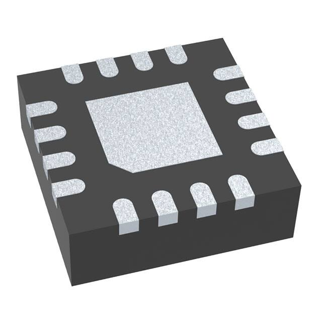
3-mm × 3-mm, 16-Pin QFN Package
•
•
•
1.0625-Gbps, 2.125-Gbps, and 4.25-Gbps
Fibre Channel Systems
High-Speed Links in Communication and
Data Systems
Backplane Interconnect
Rack-to-Rack Interconnect
A
A
A
A
A
A
A
A
A
A
DESCRIPTION
The TLK4201EA is a versatile, high-speed limiting equalizer for applications in digital high-speed links with data
rates up to 4.25 Gbps.
This device provides a high-frequency boost of 12 dB at 2.1 GHz as well as sufficient gain to ensure a fully
differential output swing for input signals as low as 100 mVP-P (at the input of the interconnect line or cable).
The high input signal dynamic range ensures low-jitter output signals even when overdriven with input signal
swings as high as 2000 mVP-P.
The TLK4201EA includes fixed loss-of-signal (LOS) detection, which can be used to implement a squelch
function by connecting the LOS output to the adjacent DISABLE input. The LOS function can be disabled by
pulling LOSDIS to high level.
The TLK4201EA is available in a small-footprint, 3-mm × 3-mm, 16-pin QFN package. It requires a single 3.3-V
supply.
This very power-efficient equalizer is characterized for operation from –40°C to 85°C.
Please be aware that an important notice concerning availability, standard warranty, and use in critical applications of Texas
Instruments semiconductor products and disclaimers thereto appears at the end of this data sheet.
PRODUCTION DATA information is current as of publication date.
Products conform to specifications per the terms of the Texas
Instruments standard warranty. Production processing does not
necessarily include testing of all parameters.
Copyright © 2006, Texas Instruments Incorporated
�TLK4201EA
www.ti.com
SLLS719 – APRIL 2006
BLOCK DIAGRAM
A simplified block diagram of the TLK4201EA is shown in Figure 1. This compact, low-power, 4.25-Gbps
equalizer consists of a high-speed data path with an offset cancellation circuitry, a loss-of-signal detection block,
and a band-gap voltage reference and bias current generation block.
The equalizer requires a single 3.3-V supply voltage. All circuit parts are described in detail as follows.
COC2
COC1
VCC
Offset
Cancellation
GND
OUTPOL
DIN+
+
+
+
+
DIN−
−
−
−
−
Gain Stage
Gain Stage
Fixed Equalizer
Stage
Gain Stage
DOUT+
CML
Output
Buffer
Stage
DOUT−
DISABLE
Bandgap Voltage
Reference and
Bias Current
Generation
Loss of
Signal Detection
LOS
LOSDIS
B0052-03
Figure 1. Simplified Block Diagram of the TLK4201EA
HIGH-SPEED DATA PATH
The high-speed data signal with frequency dependent loss is applied to the data path by means of the input
signal pins DIN+/DIN–. The data path consists of the fixed equalizer input stage with 100-Ω on-chip differential
line termination, three gain stages, which provide the required gain to ensure a limited output signal, and a CML
output stage. The equalized and amplified data output signal is available at the output pins DOUT+/DOUT–,
which provide 2 × 50-Ω back-termination to VCC. The output stage also includes a data polarity switching
function, which is controlled by the OUTPOL input, and a disable function, controlled by the signal applied to the
DISABLE input pin. An offset cancellation circuit compensates for inevitable internal offset voltages and thus
ensures proper operation even for very small input data signals.
The low-frequency cutoff is as low as 10 kHz with the built-in filter capacitor. For applications which require even
lower cutoff frequencies, an additional external filter capacitor can be connected to the COC1/COC2 pins.
LOSS OF SIGNAL DETECTION
The output signal of the second gain stage is monitored by the loss-of-signal detection circuitry. In this block, the
input signal is compared to a fixed threshold. If the low-frequency components of the input signal fall below this
threshold, a loss of signal is indicated at the LOS pin.
A squelch function can be easily implemented by connecting the LOS output to the adjacent DISABLE input.
This measure avoids chattering of the output when no input signal is present. The LOS function can be disabled
by pulling LOSDIS to high level.
BAND-GAP VOLTAGE AND BIAS GENERATION
The TLK4201EA equalizer is supplied by a single 3.3V ±10% supply voltage connected to the VCC pins. This
voltage is referred to ground (GND).
An on-chip band-gap voltage circuit generates a supply-voltage-independent reference from which all internally
required voltages and bias currents are derived.
2
Submit Documentation Feedback
�TLK4201EA
www.ti.com
SLLS719 – APRIL 2006
DEVICE INFORMATION
The TLK4201EA is available in a small-footprint, 3-mm × 3-mm, 16-pin QFN Package.
This quad package has a lead pitch of 0.5 mm. The pinout is shown in Figure 2.
VCC
1
DIN+
2
GND
COC2
COC1
NC
RGT PACKAGE
(TOP VIEW)
16
15
14
13
12
VCC
11
DOUT+
DOUT−
EP
4
9
5
6
7
8
GND
VCC
LOS
10
DISABLE
3
LOSDIS
DIN−
OUTPOL
P0019-03
Figure 2. Pinout of TLK4201EA
TERMINAL FUNCTIONS
TERMINAL
NAME
NO.
TYPE
DESCRIPTION
3.3V ± 10% supply voltage.
VCC
1, 4, 12
Supply
DIN+
2
Analog In
Noninverted data input. On-chip 100-Ω terminated to DIN–.
DIN–
3
Analog In
Inverted data input. On-chip 100-Ω terminated to DIN+.
LOSDIS
5
CMOS In
LOS disable input. High level disables LOS circuitry and sets LOS pin to low level. Low level
enables LOS function. This pin has approximately 825-kΩ internal electronic pulldown
resistor.
DISABLE
6
CMOS In
Disables CML output stage when set to high level. 400-kΩ on-chip pulldown resistor.
LOS
7
CMOS Out
High level indicates that the input signal amplitude is below the fixed threshold level.
GND
8, 16
Supply
OUTPOL
9
CMOS In
Output data signal polarity select with approximately 715-kΩ internal electronic pullup
resistor:
Setting to high-level or leaving pin open selects normal polarity. Low-level selects inverted
polarity.
DOUT–
10
CML Out
Inverted data output. On-chip 50-Ω back-terminated to VCC.
DOUT+
11
CML Out
Noninverted data output. On-chip 50-Ω back-terminated to VCC.
NC
13
—
COC1
14
Analog
Offset cancellation filter capacitor terminal 1. Connect an additional filter capacitor between
this pin and COC2 (pin 15).
To disable the offset cancellation loop connect COC1 and COC2 (pins 14 and 15).
COC2
15
Analog
Offset cancellation filter capacitor terminal 2. Connect an additional filter capacitor between
this pin and COC1 (pin 14).
To disable the offset cancellation loop connect COC1 and COC2 (pins 14 and 15).
EP
EP
Circuit ground
Not connected
Exposed die pad (EP) must be grounded.
Submit Documentation Feedback
3
�TLK4201EA
www.ti.com
SLLS719 – APRIL 2006
ABSOLUTE MAXIMUM RATINGS
over operating free-air temperature range (unless otherwise noted)
(1)
VCC (2)
VCC
Supply voltage at
VDIN+, VDIN–
Input voltage at DIN+, DIN– (2)
COC2 (2)
VALUE (1)
UNIT
–0.3 to 4
V
0.5 to 4
V
–0.3 to 4
V
±1
V
VLOSDIS, VDISABLE,
VOUTPOL, VCOC1,
VCOC2
Input voltage at LOSDIS, DISABLE, OUTPOL, COC1,
VCOC,DIFF
Differential input voltage between COC1 and COC2
VDIN,DIFF
Differential input voltage between DIN+ and DIN–
IDIN+, IDIN–
Continuous input current at input pins DIN+ and DIN–
ESD
ESD ratings at all pins, human body model (HBM)
TJ,max
Maximum junction temperature
Tstg
Storage temperature range
TA
Free-air operating temperature
–40 to 85
°C
(1)
(2)
±2.5
v
–25 to 25
mA
2.5
kV
125
°C
–65 to 85
°C
Stresses beyond those listed under "absolute maximum ratings" may cause permanent damage to the device. These are stress ratings
only, and functional operation of the device at these or any other conditions beyond those indicated under "recommended operating
conditions" is not implied. Exposure to absolute-maximum-rated conditions for extended periods may affect device reliability.
All voltage values are with respect to network ground terminal.
RECOMMENDED OPERATING CONDITIONS
over operating free-air temperature range (unless otherwise noted)
VCC
Supply voltage
VIH
High-level input voltage, CMOS
VIL
Low-level input voltage, CMOS
TA
Free-air operating temperature
MIN
NOM
MAX
3
3.3
3.6
2.1
UNIT
V
V
–40
0.6
V
85
°C
UNIT
DC ELECTRICAL CHARACTERISTICS
over recommended operating conditions (unless otherwise noted)
PARAMETER
VCC
Supply voltage
ICC
Supply current
LOSDIS = low, DISABLE = low,
including CML output current
RI
Input resistance, data
Differential
RO
Output resistance, data
Single-ended to VCC
VOH
High-level output voltage, LOS
Isource = 30 µA
VOL
Low-level output voltage, LOS
Isink = 1 mA
(1)
4
TEST CONDITIONS
Typical values are measured at VCC = 3.3 V and TA = 25°C
Submit Documentation Feedback
MIN
TYP (1)
MAX
3
3.3
3.6
V
32
38
mA
100
Ω
50
Ω
2.4
V
0.4
V
�TLK4201EA
www.ti.com
SLLS719 – APRIL 2006
AC ELECTRICAL CHARACTERISTICS
over recommended operating conditions (unless otherwise noted)
PARAMETER
Low frequency –3dB bandwidth
TYP (1)
MAX
COC = open
10
50
COC = 0.1 µF
0.8
TEST CONDITIONS
Maximum data rate
4.25
VIN,MIN
Data input voltage sensitivity (2)
BER < 10-12, input signal applied
over 36 inches of 7-mil-wide stripline
interconnect on standard FR4,
voltage at the input of the
interconnect line, K28.5 pattern at
4.25 Gbps.
VIN,MAX
Data input voltage overload
Voltage at the interconnect input
High-frequency boost
f = 2.1 GHz
Data differential output voltage
swing
DISABLE = high
VOD
DJ
Deterministic jitter
RJ
MIN
DISABLE = low
f = 4.25 GHz,
K28.5 pattern,
VIN = 200 mVP-P
(differential
voltage at the
interconnect
input)
600
kHz
Gbps
100
120
12
16
0.25
10
780
1200
2000
9
UNIT
mVP-P
mVP-P
No board or cable
20
24 inches of
7-mil-wide
stripline on
standard FR4
25
36 inches of
7-mil-wide
stripline on
standard FR4
20
30 feet CX4 cable
20
50 feet CX4 cable
35
dB
mVP-P
psP-P
Random jitter
VIN = 200 mVP-P (differential voltage
at the interconnect input)
4
Latency
From DIN+/DIN– to DOUT+/DOUT–
250
tr
Output rise time
20% to 80%, 4.25 Gbps, no board or
cable
55
85
ps
tf
Output fall time
20% to 80%, 4.25 Gbps, no board or
cable
55
85
ps
tDIS
Disable response time
VAS
VDAS
tAS/DAS
(1)
(2)
(3)
LOS assert threshold voltage
Input signal applied over 36 inches of
7-mil-wide stripline interconnect on
standard FR4, voltage at the input of
the interconnect line, K28.5 pattern at
4.25 Gbps. (3)
LOS de-assert threshold voltage
Input signal applied over 36 inches of
7-mil-wide stripline interconnect on
standard FR4, voltage at the input of
the interconnect line, K28.5 pattern at
4.25 Gbps. (3)
LOS hysteresis
K28.5 at 4.25 Gbps over 36 inches of
7-mil-wide stripline on standard FR4
3
LOS assert/de-assert time
K28.5 at 4.25 Gbps over 36 inches of
7-mil-wide stripline on standard FR4
2
40
psRMS
ps
20
ns
80
mVP-P
130
200
4.5
mVP-P
dB
100
µs
Typical values are measured at VCC = 3.3 V and TA = 25°C.
The given differential input signal swing is measured at the input of the interconnect. The high-frequency components of the signal at the
output of the interconnect (connected to input pins DIN+/DIN– of the TLK4201EA) may be attenuated by as much as 12 dB at 2.1 GHz
depending on the interconnect length and attenuation characteristics of the interconnect.
Depending on the interconnect line length and performance, the bit pattern, and the data rate, the assert and de-assert threshold
voltage levels vary. For more information, see the Typical Characteristics section.
Submit Documentation Feedback
5
�TLK4201EA
www.ti.com
SLLS719 – APRIL 2006
TYPICAL CHARACTERISTICS
Typical operating condition is at VCC = 3.3 V, TA = 25°C, and VIN = 200 mVP-P (unless otherwise noted)
DIFFERENTIAL EQUALIZER INPUT SIGNAL (TOP) AND OUTPUT SIGNAL (BOTTOM) AT
4.25 GBPS USING A PRBS 231 – 1 PATTERN
Input Voltage
75 mV/Div
36 Inches x 7 mil Stripline
Output Voltage
250 mV/Div
Output Voltage
250 mV/Div
Input Voltage
75 mV/Div
36 Inches x 7 mil Stripline
48 Inches x 7 mil Stripline
48 Inches x 7 mil Stripline
Output Voltage
250 mV/Div
Output Voltage
250 mV/Div
Input Voltage
75 mV/Div
Time − 100 ps/Div
Input Voltage
75 mV/Div
Time − 1 ns/Div
Time − 1 ns/Div
Time − 100 ps/Div
G001
Figure 3. Equalizer Input And Output Signals With Different Interconnect Lines at 4.25 GHz
6
Submit Documentation Feedback
�TLK4201EA
www.ti.com
SLLS719 – APRIL 2006
TYPICAL CHARACTERISTICS (continued)
Typical operating condition is at VCC = 3.3 V, TA = 25°C, and VIN = 200 mVP-P (unless otherwise noted)
DIFFERENTIAL EQUALIZER INPUT SIGNAL (TOP) AND OUTPUT SIGNAL (BOTTOM) AT
2.125 GBPS USING A PRBS 231 – 1 PATTERN
Input Voltage
75 mV/Div
36 Inches x 7 mil Stripline
Output Voltage
250 mV/Div
Output Voltage
250 mV/Div
Input Voltage
75 mV/Div
36 Inches x 7 mil Stripline
48 Inches x 7 mil Stripline
48 Inches x 7 mil Stripline
Output Voltage
250 mV/Div
Output Voltage
250 mV/Div
Input Voltage
75 mV/Div
Time − 100 ps/Div
Input Voltage
75 mV/Div
Time − 1 ns/Div
Time − 1 ns/Div
Time − 100 ps/Div
G002
Figure 4. Equalizer Input And Output Signals With Different Interconnect Lines at 2.125 GHz
Submit Documentation Feedback
7
�TLK4201EA
www.ti.com
SLLS719 – APRIL 2006
TYPICAL CHARACTERISTICS (continued)
Typical operating condition is at VCC = 3.3 V, TA = 25°C, and VIN = 200 mVP-P (unless otherwise noted)
DETERMINISTIC JITTER
vs
STRIPLINE LENGTH
RANDOM JITTER
vs
INPUT VOLTAGE
3.0
No Interconnect Line Loss
2.5
20
Random Jitter − psRMS
Deterministic Jitter Including PWD − psP−P
25
15
10
5
2.0
1.5
1.0
0.5
4.25 Gbps
K28.5 Pattern
0
0
5
10
15
20
25
30
35
40
45
0.0
0.0
50
0.5
Stripline Length − Inches
Figure 5.
Figure 6.
DETERMINISTIC JITTER
vs
INPUT VOLTAGE
DETERMINISTIC JITTER
vs
INPUT VOLTAGE
2.0
G004
35
Deterministic Jitter Including PWD − psP−P
Deterministic Jitter Including PWD − psP−P
35
30
25
20
15
10
No Interconnect Line Loss
4.25 Gbps
K28.5 Pattern
5
0.5
1.0
1.5
2.0
VID − Differential Input Voltage − VP−P
30
25
20
15
10
5
36−Inch 7−mil Stripline
4.25 Gbps
K28.5 Pattern
0
0.0
G005
Figure 7.
8
1.5
VID − Differential Input Voltage − VP−P
G003
0
0.0
1.0
0.5
1.0
Figure 8.
Submit Documentation Feedback
1.5
VID − Differential Input Voltage − VP−P
2.0
G006
�TLK4201EA
www.ti.com
SLLS719 – APRIL 2006
TYPICAL CHARACTERISTICS (continued)
Typical operating condition is at VCC = 3.3 V, TA = 25°C, and VIN = 200 mVP-P (unless otherwise noted)
DIFFERENTIAL OUTPUT RETURN LOSS
vs
FREQUENCY
0
0
−5
−5
−10
−10
Differential S22 − dB
Differential S11 − dB
DIFFERENTIAL INPUT RETURN LOSS
vs
FREQUENCY
−15
−20
−25
−30
−15
−20
−25
−30
−35
−35
0
1
2
3
4
5
6
0
1
f − Frequency − GHz
2
3
4
5
f − Frequency − GHz
G007
G008
Figure 9.
Figure 10.
LOS ASSERT THRESHOLD VOLTAGE
vs
DATA RATE (K28.5 PATTERN)
LOS DE-ASSERT THRESHOLD VOLTAGE
vs
DATA RATE (K28.5 PATTERN)
180
180
K28.5 Pattern
LOS De-assert Threshold Voltage − mVP−P
LOS Assert Threshold Voltage − mVP−P
K28.5 Pattern
160
140
120
36 Inch
100
6
24 Inch
48 Inch
80
60
40
12 Inch
20
160
36 Inch
48 Inch
140
120
100
80
60
40
24 Inch
12 Inch
No line
20
No line
0
1.0
1.5
2.0
2.5
3.0
3.5
4.0
4.5
0
1.0
Data Rate − Gbps
1.5
2.0
2.5
3.0
3.5
4.0
4.5
Data Rate − Gbps
G009
Figure 11.
G010
Figure 12.
Submit Documentation Feedback
9
�TLK4201EA
www.ti.com
SLLS719 – APRIL 2006
APPLICATION INFORMATION
Figure 13 shows the TLK4201EA connected with an ac-coupled interface to the data signal source via a stripline
interconnect line. The output load is ac-coupled as well.
The ac-coupling capacitors C1 through C4 in the input and output data signal lines are the only required external
components. In addition, if a very low cutoff frequency is required, as an option, an external filter capacitor COC
may be used.
NC
COC1
COC2
GND
COC
Optional
VCC
DIN+
DIN−
DIN−
VCC
DOUT+
TLK4201EA
16-Pin QFN
DOUT−
VCC
C3
C4
OUTPOL
DOUT+
DOUT−
OUTPOL
GND
C2
LOS
DIN+
VCC
DISABLE
C1
LOSDIS
0 Inch to 36 Inches
Stripline on FR4
LOSDIS
DISABLE
LOS
Optional Connection
for Squelch Function
S0072-03
Figure 13. Basic Application Circuit with AC-Coupled I/Os
0
Differential Stripline Attenuation − dB
−5
12” Stripline
−10
−15
−20
−25
24” Stripline
−30
−35
36” Stripline
−40
−45
48” Stripline
−50
−55
−60
0
1
2
3
4
5
6
f − Frequency − GHz
G011
Figure 14. Attenuation Characteristics of Stripline Interconnect Lines
10
Submit Documentation Feedback
�PACKAGE OPTION ADDENDUM
www.ti.com
10-Dec-2020
PACKAGING INFORMATION
Orderable Device
Status
(1)
Package Type Package Pins Package
Drawing
Qty
Eco Plan
(2)
Lead finish/
Ball material
MSL Peak Temp
Op Temp (°C)
Device Marking
(3)
(4/5)
(6)
TLK4201EARGTR
ACTIVE
VQFN
RGT
16
3000
RoHS & Green
NIPDAU
Level-2-260C-1 YEAR
-40 to 85
420E
TLK4201EARGTT
ACTIVE
VQFN
RGT
16
250
RoHS & Green
NIPDAU
Level-2-260C-1 YEAR
-40 to 85
420E
(1)
The marketing status values are defined as follows:
ACTIVE: Product device recommended for new designs.
LIFEBUY: TI has announced that the device will be discontinued, and a lifetime-buy period is in effect.
NRND: Not recommended for new designs. Device is in production to support existing customers, but TI does not recommend using this part in a new design.
PREVIEW: Device has been announced but is not in production. Samples may or may not be available.
OBSOLETE: TI has discontinued the production of the device.
(2)
RoHS: TI defines "RoHS" to mean semiconductor products that are compliant with the current EU RoHS requirements for all 10 RoHS substances, including the requirement that RoHS substance
do not exceed 0.1% by weight in homogeneous materials. Where designed to be soldered at high temperatures, "RoHS" products are suitable for use in specified lead-free processes. TI may
reference these types of products as "Pb-Free".
RoHS Exempt: TI defines "RoHS Exempt" to mean products that contain lead but are compliant with EU RoHS pursuant to a specific EU RoHS exemption.
Green: TI defines "Green" to mean the content of Chlorine (Cl) and Bromine (Br) based flame retardants meet JS709B low halogen requirements of


 工商网监
湘ICP备2023018690号
工商网监
湘ICP备2023018690号
