Product
Folder
Order
Now
Support &
Community
Tools &
Software
Technical
Documents
TLV4021, TLV4031, TLV4041, TLV4051
SNVSB04B – MARCH 2019 – REVISED JUNE 2020
TLV40x1 Small-Size, Low-Power Comparator with Precision Reference
1 Features
3 Description
•
•
•
•
The TLV40x1 devices are low-power, high-accuracy
comparators with precision references and fast
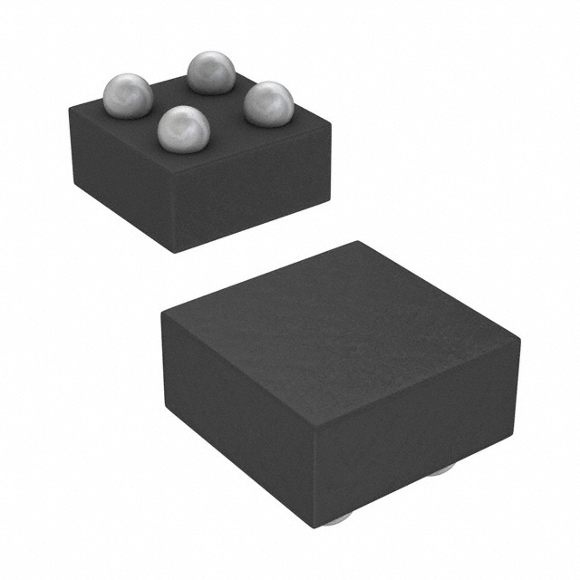
response. The comparators are available in an ultrasmall, DSBGA package measuring 0.73 mm × 0.73
mm, making the TLV40x1 applicable for space-critical
designs like portable or battery-powered electronics
where low-power and fast response to changes in
operating conditions is required.
1
•
•
•
•
•
•
•
•
Wide supply voltage range: 1.6 V to 5.5 V
Precision References: 0.2 V, 0.5 V, and 1.2 V
Fixed threshold of 3.2 V
Reference accuracy
– 0.5% at 25°C
– 1% over temperature
Low quiescent current: 2 µA
Propagation delay: 360 ns
Push-pull and open-drain output options
Known startup conditions
Non-inverting and inverting input options
Precision hysteresis
Temperature range: –40°C to +125°C
Packages:
– 0.73 mm × 0.73 mm DSBGA (4-bump)
– SOT-23 (5-pin)
The factory-trimmed references and precision
hysteresis combine to make the TLV40x1 appropriate
for voltage and current monitoring in harsh, noisy
environments where slow moving input signals must
be converted into clean digital outputs. Similarly, brief
glitches on the input are rejected ensuring stable
output operation without false triggering.
The TLV40x1 are available in multiple configurations
allowing system designers to achieve their desired
output response. For example, the TLV4021 and
TLV4041 offer a non-inverting input, while the
TLV4031 and TLV4051 have an inverting input.
Furthermore, the TLV4021 and TLV4031 feature an
open-drain output stage, while the TLV4041 and
TLV4051 feature a push-pull output stage. Lastly,
each comparator in the TLV40x1 family is available
with a 0.2V, 0.5V, or 1.2V precision reference.
2 Applications
•
•
•
•
•
•
•
•
Mobile phones and tablets
Headsets/headphones & earbuds
PC & notebooks
Gas detector
Smoke & heat detector
Motion detector
Gas meter
Servo drive position sensor
Device Information
PART NUMBER
PACKAGE
(1)
BODY SIZE (NOM)
TLV4021, TLV4031,
TLV4041, TLV4051
DSBGA (4)
0.73 mm × 0.73 mm
TLV4041, TLV4051
SOT-23 (5)
2.9 mm × 1.6 mm
(1) For all available packages, see the orderable addendum at
the end of the data sheet.
TLV40x1 Configurations
Non-Inverting
Inverting
V+
IN
IN
V+
OUT
IN
t
t
+
TLV4021
TLV4041
+
TLV4031
TLV4051
REF
s5
V+
OUT
+
REF
Fixed Threshold
s5
t
TLV4021S5
1.2V
s5
1
An IMPORTANT NOTICE at the end of this data sheet addresses availability, warranty, changes, use in safety-critical applications,
intellectual property matters and other important disclaimers. UNLESS OTHERWISE NOTED, this document contains PRODUCTION
DATA.
�TLV4021, TLV4031, TLV4041, TLV4051
SNVSB04B – MARCH 2019 – REVISED JUNE 2020
www.ti.com
Table 1. TLV40x1 Truth Table
DEVICE
Input Configuration
Reference
TLV4021R1
TLV4041R5
Non-Inverting
Push-Pull
Open-Drain
0.2 V
TLV4041R2
TLV4031R1
Push-Pull
Open-Drain
1.2 V
TLV4051R1
TLV4051R5
Inverting
Push-Pull
0.5 V
TLV4031R2
Push-Pull
Open-Drain
0.2 V
TLV4051R2
Push-Pull
DEVICE
Input Configuration
Fixed Threshold
Output Type
TLV4021S5
Non-Inverting
3.2 V
Open-Drain
VPU
VPU
TLV4021R2
TLV4041R2
TLV4021R1
IN
OUT
+
IN
t
OUT
+
t
t
1.2V
s5
VPU
VPU
TLV4051R2
TLV4031R1
V+
V+
t
OUT
IN
t
+
IN
OUT
OUT
1.2V
s5
t
+
s5
s5
IN
0.2V
1.2V
0.2V
V+
+
V+
TLV4051R1
t
TLV4031R2
OUT
OUT
+
s5
s5
s5
IN
0.2V
1.2V
0.2V
V+
+
OUT
t
TLV4041R1
V+
V+
V+
IN
Push-Pull
0.5 v
TLV4021R2
+
Open-Drain
1.2 V
TLV4041R1
IN
Output Type
s5
VPU
TLV4041R5
TLV4051R5
TLV4021S5
V+
V+
V+
t
OUT
+
t
1.2V
1.2V
s5
IN
t
IN
+
OUT
+
IN
1.2V
s5
s5
2
Submit Documentation Feedback
Copyright © 2019–2020, Texas Instruments Incorporated
Product Folder Links: TLV4021 TLV4031 TLV4041 TLV4051
�TLV4021, TLV4031, TLV4041, TLV4051
www.ti.com
SNVSB04B – MARCH 2019 – REVISED JUNE 2020
Table of Contents
1
2
3
4
5
6
7
Features ..................................................................
Applications ...........................................................
Description .............................................................
Revision History.....................................................
Pin Configuration and Functions .........................
Specifications.........................................................
1
1
1
3
4
5
6.1
6.2
6.3
6.4
6.5
6.6
6.7
5
5
5
5
6
8
9
Absolute Maximum Ratings ......................................
ESD Ratings..............................................................
Recommended Operating Conditions.......................
Thermal Information ..................................................
Electrical Characteristics...........................................
Switching Characteristics ..........................................
Typical Characteristics ..............................................
Detailed Description ............................................ 15
7.1 Overview ................................................................. 15
7.2 Functional Block Diagram ....................................... 16
7.3 Feature Description................................................. 17
7.4 Device Functional Modes........................................ 17
8
Application and Implementation ........................ 20
8.1 Application Information............................................ 20
8.2 Typical Application .................................................. 22
8.3 What to Do and What Not to Do ............................ 24
9 Power Supply Recommendations...................... 25
10 Layout................................................................... 25
10.1 Layout Guidelines ................................................. 25
10.2 Layout Example .................................................... 25
11 Device and Documentation Support ................. 26
11.1
11.2
11.3
11.4
11.5
11.6
Related Links ........................................................
Receiving Notification of Documentation Updates
Community Resources..........................................
Trademarks ...........................................................
Electrostatic Discharge Caution ............................
Glossary ................................................................
26
26
26
26
26
26
12 Mechanical, Packaging, and Orderable
Information ........................................................... 27
4 Revision History
Changes from Revision A (May 2019) to Revision B
Page
•
Added SOT-23 package option with 0.5V reference. ............................................................................................................ 1
•
Changed configuration diagram and TLV40x1 Truth Table. ................................................................................................. 1
•
Added Configuration diagrams for entire TLV40x1 family...................................................................................................... 2
Changes from Original (October 2018) to Revision A
•
Page
Changed Product Preview to Production Data ...................................................................................................................... 1
Copyright © 2019–2020, Texas Instruments Incorporated
Submit Documentation Feedback
Product Folder Links: TLV4021 TLV4031 TLV4041 TLV4051
3
�TLV4021, TLV4031, TLV4041, TLV4051
SNVSB04B – MARCH 2019 – REVISED JUNE 2020
www.ti.com
5 Pin Configuration and Functions
YKA Package
4-Bump DSBGA
Top View
Top View
A
OUT
IN
B
V+
V-
1
2
DSBGA Package Pin Functions
PIN
I/O
DESCRIPTION
NAME
NUMBER
OUT
A1
O
Comparator output: OUT is push-pull on TLV4041/4051 and open-drain on TLV4021/4031
V+
B1
P
Positive (highest) power supply
V–
B2
P
Negative (lowest) power supply
IN
A2
I
Comparator input: IN is non-Inverting on TLV4021/4041 and inverting on TLV4031/4051
SOT-23 Package
5-pin
Top View
Top View
V+
1
V-
2
NC
3
5
OUT
4
IN
SOT-23 Pin Functions
PIN
4
I/O
DESCRIPTION
NAME
NUMBER
V+
1
P
Positive (highest) power supply
V–
2
P
Negative (lowest) power supply
NC
3
x
No connect; this pin is not internally connected to the die. It can be grounded if that is preferred
in the system.
IN
4
I
Comparator input: IN is inverting on TLV4051
OUT
5
O
Comparator output: OUT is push-pull
Submit Documentation Feedback
Copyright © 2019–2020, Texas Instruments Incorporated
Product Folder Links: TLV4021 TLV4031 TLV4041 TLV4051
�TLV4021, TLV4031, TLV4041, TLV4051
www.ti.com
SNVSB04B – MARCH 2019 – REVISED JUNE 2020
6 Specifications
6.1 Absolute Maximum Ratings
over operating free-air temperature range (unless otherwise noted) (1)
Supply voltage: VS = (V+) – (V–)
Input voltage (IN) from (V–)
(2)
MIN
MAX
–0.3
6
–0.3
6
Input Current (IN) (2)
–0.3
6
V
TLV4041, TLV4051
–0.3
(V+) + 0.3
V
Junction temperature, TJ
Storage temperature, Tstg
(3)
V
mA
TLV4021, TLV4031
Output short-circuit duration (3)
(2)
V
±10
Output voltage (OUT) from (V-)
(1)
UNIT
–65
10
s
150
°C
150
°C
Stresses beyond those listed under Absolute Maximum Ratings may cause permanent damage to the device. These are stress ratings
only, which do not imply functional operation of the device at these or any other conditions beyond those indicated under Recommended
Operating Conditions. Exposure to absolute-maximum-rated conditions for extended periods may affect device reliability.
Input terminals are diode-clamped to (V–). Input signals that can swing more than 0.3 V below (V–) must be current-limited to 10 mA or
less.
In addition, IN can be greater than (V+) and OUT as long as it is within the –0.3 V to 6 V range. Input signals that can swing beyond this
range must be current-limited to 10 mA or less.
Short-circuit to ground.
6.2 ESD Ratings
VALUE
V(ESD)
(1)
(2)
Electrostatic
discharge
Human-body model (HBM), per ANSI/ESDA/JEDEC JS-001 (1)
±2000
Charged-device model (CDM), per JEDEC specification JESD22-C101 (2)
±1000
UNIT
V
JEDEC document JEP155 states that 500-V HBM allows safe manufacturing with a standard ESD control process.
JEDEC document JEP157 states that 250-V CDM allows safe manufacturing with a standard ESD control process.
6.3 Recommended Operating Conditions
over operating free-air temperature range (unless otherwise noted)
MIN
MAX
Supply voltage: VS = (V+) – (V–)
1.6
5.5
UNIT
V
Ambient temperature, TA
–40
125
°C
6.4 Thermal Information
TLV40x1
THERMAL METRIC
(1)
YKA (DSBGA)
SOT-23 (DBV)
4 BUMPS
5 PINS
UNIT
RθJA
Junction-to-ambient thermal resistance
205.5
181.7
°C/W
RθJC(top)
Junction-to-case (top) thermal resistance
1.8
101.1
°C/W
RθJB
Junction-to-board thermal resistance
75.3
52.0
°C/W
ψJT
Junction-to-top characterization parameter
0.9
28.2
°C/W
ψJB
Junction-to-board characterization parameter
74.7
51.6
°C/W
RθJC(bot)
Junction-to-case (bottom) thermal resistance
N/A
N/A
°C/W
(1)
For more information about traditional and new thermal metrics, see the Semiconductor and IC Package Thermal Metrics application
report.
Copyright © 2019–2020, Texas Instruments Incorporated
Submit Documentation Feedback
Product Folder Links: TLV4021 TLV4031 TLV4041 TLV4051
5
�TLV4021, TLV4031, TLV4041, TLV4051
SNVSB04B – MARCH 2019 – REVISED JUNE 2020
www.ti.com
6.5 Electrical Characteristics
VS = 1.8 V to 5 V, typical values are at TA = 25°C.
PARAMETER
VIT+
VIT-
VIT+
VIT-
VIT+
VIT-
VIT+
VIT(1)
VHYS
VHYS
(1)
VHYS
TEST CONDITIONS
TYP
MAX
1.194
1.2
1.206
UNIT
VS = 1.8 V and 5 V, TA = 25°C
Postive-going input threshold
voltage
VS = 1.8 V and 5 V, TA = -40℃ to +125℃
Negative-going input
threshold voltage
VS = 1.8 V and 5 V, TA = 25°C
1.174
Negative-going input
threshold voltage
VS = 1.8 V and 5 V, TA = -40°C to +125°C
1.168
Postive-going input threshold
voltage
VS = 1.8 V and 5 V, TA = 25°C
0.197
Postive-going input threshold
voltage
VS = 1.8 V and 5 V, TA = -40℃ to +125℃
Negative-going input
threshold voltage
VS = 1.8 V and 5 V, TA = 25°C
0.177
Negative-going input
threshold voltage
VS = 1.8 V and 5 V, TA = -40°C to +125°C
0.176
Postive-going input threshold
voltage
(TLV40x1R5 only)
VS = 1.8 V and 5 V, TA = 25°C
0.495
Postive-going input threshold
voltage
(TLV40x1R5 only)
VS = 1.8 V and 5 V, TA = -40℃ to +125℃
Negative-going input
threshold voltage
(TLV40x1R5 only)
VS = 1.8 V and 5 V, TA = 25°C
0.4752
Negative-going input
threshold voltage
(TLV40x1R5 only)
VS = 1.8 V and 5 V, TA = -40°C to +125°C
0.4704
Postive-going input threshold
voltage
VS = 1.8 V and 5 V, TA = 25°C
Postive-going input threshold
voltage
VS = 1.8 V and 5 V, TA = -40℃ to +125℃
Negative-going input
threshold voltage
VS = 1.8 V and 5 V, TA = 25°C
3.184
Negative-going input
threshold voltage
VS = 1.8 V and 5 V, TA = -40℃ to +125℃
3.168
Input hysteresis voltage
VS = 1.8 V and 5 V, TA = 25℃
TLV40x1Ry
20
mV
Input hysteresis voltage
(TLV40x1R5 only)
VS = 1.8 V and 5 V, TA = 25℃
TLV40x1R5
20
mV
TLV40x1S5
1.212
V
1.18
1.186
1.192
0.2
0.196
0.203
0.204
TLV40x1R2
V
0.18
0.183
0.184
0.5
0.49
0.505
V
0.51
V
0.4848
V
0.4896
V
3.270
V
3.287
V
3.216
V
3.232
V
TLV40x1R5
3.238
0.48
3.254
3.221
TLV4021S5
Input hysteresis voltage
VS = 1.8 V and 5 V, TA = 25°C
Input voltage range
TA = -40℃ to +125℃
IBIAS
Input bias current
Over VIN range
IBIAS
Input bias current
(TLV4021S5 only)
IN = 3.3 V
VOL
Voltage output swing
from (V–)
Voltage output swing
from (V+)
(TLV4041/4051 only)
1.188
TLV40x1R1
VIN
VOH
MIN
Postive-going input threshold
voltage
3.2
54
V–
mV
5.5
V
10
pA
1.65
µA
ISINK = 200 µA, OUT asserted low,
VS = 5 V, TA = –40°C to +125°C
100
mV
ISINK = 3 mA, OUT asserted low,
VS = 5 V, TA = –40°C to +125°C
400
mV
ISOURCE = 200 µA, OUT asserted high,
VS = 5 V, TA = –40°C to +125°C
100
mV
ISOURCE = 3 mA, OUT asserted high,
VS = 5 V, TA = –40°C to +125°C
400
mV
IO-LKG
Open-drain output leakage
current
(TLV4021/4031 only)
VS = 5 V, OUT asserted high
VPULLUP = (V+), TA = 25°C
20
pA
ISC
Short-circuit current
VS = 5 V, sinking, TA = 25°C
55
mA
Short-circuit current
VS = 5 V, sourcing, TA = 25°C
(TLV4041/4051 only)
50
mA
ISC
(1)
6
See Section 7.4.3 (Switching Thresholds and Hysteresis) for more details.
Submit Documentation Feedback
Copyright © 2019–2020, Texas Instruments Incorporated
Product Folder Links: TLV4021 TLV4031 TLV4041 TLV4051
�TLV4021, TLV4031, TLV4041, TLV4051
www.ti.com
SNVSB04B – MARCH 2019 – REVISED JUNE 2020
Electrical Characteristics (continued)
VS = 1.8 V to 5 V, typical values are at TA = 25°C.
PARAMETER
IQ
Quiescent current
VPOR (2)
Power-on reset voltage
(2)
TEST CONDITIONS
MIN
No load, TA = 25°C, Output Low, VS = 1.8 V
TYP
MAX
2
3.5
µA
5
µA
No load, TA = –40°C to +125°C, Output Low, VS = 1.8 V
1.45
UNIT
V
See Section 7.4.1 (Power ON Reset) for more details.
Copyright © 2019–2020, Texas Instruments Incorporated
Submit Documentation Feedback
Product Folder Links: TLV4021 TLV4031 TLV4041 TLV4051
7
�TLV4021, TLV4031, TLV4041, TLV4051
SNVSB04B – MARCH 2019 – REVISED JUNE 2020
www.ti.com
6.6 Switching Characteristics
Typical values are at TA = 25°C, VS = 3.3 V, CL = 15 pF; Input overdrive = 100 mV for TLV40x1Ry & 5% for
TLV4021S5, RP=4.99 kΩ for open-drain options (unless otherwise noted).
PARAMETER
TEST CONDITIONS
MIN
TYP
MAX
UNIT
tPHL
Propagation delay, high-to-low
(1)
Midpoint of input to midpoint of output
360
ns
tPLH
Propagation delay, low-to-high
(1)
Midpoint of input to midpoint of output
360
ns
tPHL
Propagation delay, high-to-low
(1)
(TLV4021S5 only)
Midpoint of input to midpoint of output
2
µs
tPLH
Propagation delay, low-tohigh (1)(TLV4021S5 only)
Midpoint of input to midpoint of output
2
µs
tR
Rise time
(TLV4041/4051 only)
20% to 80%
10
ns
tF
Fall time
20% to 80%
tON
Power-up time
(1)
(2)
(2)
10
ns
500
µs
High-to-low and low-to-high refers to the transition at the input.
During power on cycle, VS must exceed 1.6 V for tON before the output will reflect the condition on the input. Prior to tON elapsing, the
output is controlled by the POR circuit.
VIT+
VHYS
V/d5
IN
tPHL
tPLH
OUT
Figure 1. Timing Diagram Non-Inverting Input
8
Submit Documentation Feedback
Copyright © 2019–2020, Texas Instruments Incorporated
Product Folder Links: TLV4021 TLV4031 TLV4041 TLV4051
�TLV4021, TLV4031, TLV4041, TLV4051
www.ti.com
SNVSB04B – MARCH 2019 – REVISED JUNE 2020
6.7 Typical Characteristics
at TJ = 25°C and VS = 3.3 V (unless otherwise noted)
1.2012
VS = 1.8V
VS = 3.3V
VS = 5.0V
1.2009
1.2006
Device Count
VIT+ (V)
1.2003
1.2
1.1997
1.1994
1.1991
1.1988
1.1985
-40
-20
0
20
40
60
80
Temperature (°C)
100
120
140
TLV40x1R1
21000
19500
18000
16500
15000
13500
12000
10500
9000
7500
6000
4500
3000
1500
0
1.198
1.1986
VS = 1.8V
VS = 3.3V
VS = 5.0V
1.1808
1.1805
Device Count
VIT- (V)
1.1802
1.1799
1.1796
1.1793
1.179
1.1787
1.1784
0
20
40
60
80
Temperature (°C)
100
120
140
TLV40x1R1
21000
19500
18000
16500
15000
13500
12000
10500
9000
7500
6000
4500
3000
1500
0
1.1778
Figure 4. Negative Threshold vs Temperature
VS = 5 V
1.1784
1.179
1.1796 1.1802
VIT- (V)
1.1808
1.1814
VS = 5 V
Figure 5. Negative Threshold Histogram
20000
VS = 1.8V
VS = 3.3V
VS = 5.0V
20.56
20.48
18000
16000
14000
Device Count
20.4
VHYST (mV)
1.2016
TLV40x1R1
20.64
20.32
20.24
20.16
12000
10000
8000
6000
20.08
4000
20
2000
19.92
-40
1.201
Figure 3. Positive Threshold Histogram
1.1811
-20
1.1998 1.2004
VIT+ (V)
TLV40x1R1
Figure 2. Positive Threshold vs Temperature
1.1781
-40
1.1992
-20
0
20
40
60
80
Temperature (°C)
100
120
TLV40x1R1
140
0
17
18
19
20
VHYST (mV)
21
TLV40x1R1
Figure 6. Hysteresis vs Temperature
Copyright © 2019–2020, Texas Instruments Incorporated
22
23
VS = 5 V
Figure 7. Hysteresis Histogram
Submit Documentation Feedback
Product Folder Links: TLV4021 TLV4031 TLV4041 TLV4051
9
�TLV4021, TLV4031, TLV4041, TLV4051
SNVSB04B – MARCH 2019 – REVISED JUNE 2020
www.ti.com
Typical Characteristics (continued)
at TJ = 25°C and VS = 3.3 V (unless otherwise noted)
30000
0.2004
VS = 1.8V
VS = 3.3V
VS = 5.0V
0.20025
27000
24000
0.2001
Device Count
21000
VIT+ (V)
0.19995
0.1998
0.19965
18000
15000
12000
9000
0.1995
6000
0.19935
3000
0.1992
-40
-20
0
20
40
60
80
Temperature (°C)
100
120
0
0.198
140
TLV40x1R2
Figure 8. Positive Threshold vs Temperature
VS = 5 V
27000
24000
Device Count
VIT- (V)
0.2016
21000
0.17992
0.17984
0.17976
0.17968
18000
15000
12000
9000
0.1796
6000
0.17952
3000
-20
0
20
40
60
80
Temperature (°C)
100
120
0
0.1776
140
TLV40x1R2
0.1784
0.1792
0.18
VIT- (V)
0.1808
0.1816
TLV40x1R2
Figure 10. Negative Threshold vs Temperature
VS = 5 V
Figure 11. Negative Threshold Histogram
500
20.22
VS = 1.8V
VS = 3.3V
VS = 5.0V
20.2
20.18
450
400
20.16
350
20.14
Device Count
VHYST (mV)
0.201
Figure 9. Positive Threshold Histogram
VS = 1.8V
VS = 3.3V
VS = 5.0V
0.18
20.12
20.1
20.08
300
250
200
150
20.06
20.04
100
20.02
50
-20
0
20
40
60
80
Temperature (°C)
100
120
TLV40x1R2
140
0
17
18
19
20
VHYST (mV)
21
22
TLV40x1R2
Figure 12. Hysteresis vs Temperature
10
0.1998 0.2004
VIT+ (V)
30000
0.18008
20
-40
0.1992
TLV40x1R2
0.18016
0.17944
-40
0.1986
Submit Documentation Feedback
23
VS = 5 V
Figure 13. Hysteresis Histogram
Copyright © 2019–2020, Texas Instruments Incorporated
Product Folder Links: TLV4021 TLV4031 TLV4041 TLV4051
�TLV4021, TLV4031, TLV4041, TLV4051
www.ti.com
SNVSB04B – MARCH 2019 – REVISED JUNE 2020
Typical Characteristics (continued)
3.2545
3.254
3.2535
3.253
3.2525
3.252
3.2515
3.251
3.2505
3.25
3.2495
3.249
3.2485
3.248
-40
25000
22500
20000
17500
Device Count
VIT+ (V)
at TJ = 25°C and VS = 3.3 V (unless otherwise noted)
15000
12500
10000
7500
5000
VS = 1.8V
VS = 3.3V
VS = 5.0V
-20
0
20
40
60
80
Temperature (°C)
100
120
2500
0
3.2475
140
TLV4021S5
3.2565
3.2595
Figure 15. Positive Threshold Histogram
25000
22500
20000
17500
Device Count
VIT- (mV)
3.2535
VIT+ (V)
TLV4021S5
Figure 14. Positive Threshold vs Temperature
3.2015
3.201
3.2005
3.2
3.1995
3.199
3.1985
3.198
3.1975
3.197
3.1965
3.196
3.1955
3.195
3.1945
-40
3.2505
15000
12500
10000
7500
5000
VS = 1.8V
VS = 3.3V
VS = 5.0V
-20
0
20
40
60
80
Temperature (°C)
100
120
2500
0
3.196
140
TLV4021S5
3.1975
3.199
3.2005
VIT- (V)
3.202
3.2035
3.205
TLV4021S5
Figure 16. Negative Threshold vs Temperature
Figure 17. Negative Threshold Histogram
53.8
18000
16000
53.6
14000
Device Count
VHYST (mV)
53.4
53.2
53
52.8
-40°C
25°C
85°C
125°C
52.6
52.4
1.5
2
2.5
3
3.5
VS (V)
4
4.5
5
TLV4021S5
5.5
12000
10000
8000
6000
4000
2000
0
45 46 47 48 49 50 51 52 53 54 55 56 57 58 59 60 61 62
Hysteresis (mV)
TLV4021S5
Figure 18. Hysteresis vs Supply Voltage
Copyright © 2019–2020, Texas Instruments Incorporated
Figure 19. Hysteresis Histogram
Submit Documentation Feedback
Product Folder Links: TLV4021 TLV4031 TLV4041 TLV4051
11
�TLV4021, TLV4031, TLV4041, TLV4051
SNVSB04B – MARCH 2019 – REVISED JUNE 2020
www.ti.com
Typical Characteristics (continued)
5000
5000
1000
1000
100
100
10
1
-40°C
25°C
85°C
125°C
0.1
IO-LKG (pA)
IBIAS (pA)
at TJ = 25°C and VS = 3.3 V (unless otherwise noted)
1
0.01
0.2
0.3
0.5 0.7 1
VIN (V)
VS = 1.8V to 5V
2
3
0.001
-40
4 5 6 7 8 10
20
40
60
80
Temperature (°C)
100
120
140
Figure 21. Output Current Leakage vs Temperature
2
2
1
1
0.7
0.5
0.5
0.3
0.2
0.1
0.05
0.03
0.02
-40°C
0°C
25°C
125°C
0.005
0.1
0.2 0.3 0.5
0.3
0.2
0.1
0.07
0.05
-40°C
0°C
25°C
125°C
0.03
0.02
0.01
0.1
1
2 3 4 5 67 10
20 30 50 70100
Output Sinking Current (mA)
VS = 1.8V
0.2 0.3 0.5
1
2 3 4 5 67 10
20 30 50 70100
Output Sourcing Current (mA)
VS = 1.8V
Figure 22. Output Voltage vs Output Sinking Current
Figure 23. Output Voltage vs Output Sourcing Current
5
3
2
1
0.5
0.3
0.2
0.1
0.05
0.03
0.02
-40°C
0°C
25°C
125°C
0.01
0.005
0.1
0.2 0.3 0.5
1
2 3 4 5 67 10
20 30 50 70100
Output Sinking Current (mA)
VS = 3.3V
Output Voltage from V+ (V)
5
3
2
Output Voltage from V- (V)
0
Figure 20. Bias Current vs Common Mode Voltage
0.01
1
0.5
0.3
0.2
0.1
0.05
0.03
0.02
-40°C
0°C
25°C
125°C
0.01
0.005
0.1
0.2 0.3 0.5
1
2 3 4 5 67 10
20 30 50 70100
Output Sourcing Current (mA)
VS = 3.3V
Figure 24. Output Voltage vs Output Sinking Current
12
-20
TLV40x1Ry
Output Voltage from V+ (V)
Output Voltage from V- (V)
10
0.1
0.01
0.001
0.1
VS = 1.8V
VS = 3.3V
VS = 5V
Submit Documentation Feedback
Figure 25. Output Voltage vs Output Sourcing Current
Copyright © 2019–2020, Texas Instruments Incorporated
Product Folder Links: TLV4021 TLV4031 TLV4041 TLV4051
�TLV4021, TLV4031, TLV4041, TLV4051
www.ti.com
SNVSB04B – MARCH 2019 – REVISED JUNE 2020
Typical Characteristics (continued)
at TJ = 25°C and VS = 3.3 V (unless otherwise noted)
10
5
5
Output Voltage from V- (V)
2
1
0.5
0.2
0.1
0.05
-40°C
0°C
25°C
125°C
0.02
0.01
0.005
0.1
0.2 0.3 0.5
Output Voltage from V+ (V)
10
2
1
0.5
0.2
0.1
0.05
0.01
0.005
0.1
1
2 3 4 5 67 10
20 30 50 70100
Output Sinking Current (mA)
VS = 5V
Figure 26. Output Voltage vs Output Sinking Current
Figure 27. Output Voltage vs Output Sourcing Current
3
2.8
tpLH (ns)
IQ (uA)
2.6
2.4
2.2
2
1.8
VS = 1.8V
VS = 3.3V
VS = 5V
1.6
-20
0.2 0.3 0.5
1
2 3 4 5 67 10
20 30 50 70100
Output Sourcing Current (mA)
VS = 5V
3.2
1.4
-40
-40°C
0°C
25°C
125°C
0.02
0
20
40
60
80
Temperature (°C)
100
120
1500
1400
1300
1200
1100
1000
900
800
700
600
500
400
300
200
-40°C
25°C
85°C
125°C
0
140
20
40
60
80
100 120 140 160 180 200 220
VOD (mV)
VS = 1.8V to 5V
Figure 28. Supply Current vs Temperature
Figure 29. Propagation Delay Low-High vs Input Overdrive
6
2400
-40°C
25°C
85°C
125°C
2200
2000
1800
-40°C
25°C
85°C
125°C
5.5
5
4.5
tpLH (us)
1600
tpHL (ns)
TLV40x1R2
1400
1200
1000
4
3.5
3
2.5
800
600
2
400
1.5
200
1
0
20
40
60
80
100 120 140 160 180 200 220
VOD (mV)
VS = 1.8V to 5V
TLV40x1R2
Figure 30. Propagation Delay High-Low vs Input Overdrive
Copyright © 2019–2020, Texas Instruments Incorporated
0
1
2
3
4
VS = 1.8V to 5V
5
6
VOD (%)
7
8
9
10
11
TLV4021S5
Figure 31. Propagation Delay Low-High vs Input Overdrive
Submit Documentation Feedback
Product Folder Links: TLV4021 TLV4031 TLV4041 TLV4051
13
�TLV4021, TLV4031, TLV4041, TLV4051
SNVSB04B – MARCH 2019 – REVISED JUNE 2020
www.ti.com
Typical Characteristics (continued)
tpHL (us)
at TJ = 25°C and VS = 3.3 V (unless otherwise noted)
7.5
7
6.5
6
5.5
5
4.5
4
3.5
3
2.5
2
1.5
1
-40°C
25°C
85°C
125°C
0
1
2
3
4
5
6
VOD (%)
7
8
9
10
11
VS = 1.8V to 5V
TLV4021S5
Figure 32. Propagation Delay High-Low vs Input Overdrive
14
Submit Documentation Feedback
Copyright © 2019–2020, Texas Instruments Incorporated
Product Folder Links: TLV4021 TLV4031 TLV4041 TLV4051
�TLV4021, TLV4031, TLV4041, TLV4051
www.ti.com
SNVSB04B – MARCH 2019 – REVISED JUNE 2020
7 Detailed Description
7.1 Overview
The TLV40x1 devices are low-power comparators that are well suited for compact, low-current, precision voltage
detection applications. With high-accuracy, switching thresholds options of 0.2V, 0.5 V, 1.2V, and 3.2V, 2uA of
quiescent current, and propagation delay of 450ns and 2us, the TLV40x1 comparator family enables power
conscious systems to monitor and respond quickly to fault conditions.
The TLV40x1Ry comparators assert the output signal as shown in Table 2. VIT+ represents the positive-going
input threshold that causes the comparator output to change state, while VIT- represents the negative-going input
threshold that causes the output to change state. Since VIT+ and VIT- are factory trimmed and warranted over
temperature, the TLV40x1 is equally suited for undervoltage and overvoltage applications. In order to monitor
any voltage above the internal reference voltage, an external resistor divider network is required.
The TLV4021S5 functions similar to the TLV40x1Ry comparators except the resistor divider is internal to the
device. Having the resistor divider internal to the device allows the TLV4021S5 to have switching thresholds
higher than the internal reference voltage of 1.2V without any external components.
Table 2. TLV40x1 Truth Table
DEVICE
(VIT+, VIT-)
OUTPUT
TOPOLOGY
TLV4021R2
TLV4021R1
0.2V, 0.18V
1.2V, 1.18V
TLV4041R2
TLV4041R5
TLV4041R1
0.2V, 0.18V
0.5V, 0.48V
1.2V, 1.18V
Push-Pull
TLV4031R2
TLV4031R1
0.2V, 0.18V
1.2V, 1.18V
Open-Drain
TLV4051R2
TLV4051R5
TLV4051R1
0.2V, 0.18V
0.5V, 0.48V
1.2V, 1.18V
Push-Pull
TLV4021S5
3.254V, 3.2V
Open-Drain
Copyright © 2019–2020, Texas Instruments Incorporated
Open-Drain
INPUT VOLTAGE
OUTPUT LOGIC LEVEL
IN > VIT+
Output high impedance
IN < VIT-
Output asserted low
IN > VIT+
Output asserted high
IN < VIT-
Output asserted low
IN > VIT+
Output asserted low
IN < VIT-
Output high impedance
IN > VIT+
Output asserted low
IN < VIT-
Output asserted high
IN > VIT+
Output high impedance
IN < VIT-
Output asserted low
Submit Documentation Feedback
Product Folder Links: TLV4021 TLV4031 TLV4041 TLV4051
15
�TLV4021, TLV4031, TLV4041, TLV4051
SNVSB04B – MARCH 2019 – REVISED JUNE 2020
www.ti.com
7.2 Functional Block Diagram
VPU
VPU
TLV4021R2
IN
t
OUT
+
OUT
+
t
t
1.2V
s5
VPU
VPU
TLV4051R2
TLV4031R1
V+
V+
t
OUT
IN
t
+
IN
OUT
OUT
1.2V
s5
t
+
s5
s5
IN
0.2V
1.2V
0.2V
V+
+
V+
TLV4051R1
t
TLV4031R2
OUT
OUT
+
s5
s5
s5
IN
0.2V
1.2V
0.2V
IN
IN
t
V+
+
OUT
+
TLV4041R1
V+
V+
V+
IN
TLV4041R2
TLV4021R1
s5
VPU
TLV4041R5
TLV4051R5
TLV4021S5
V+
V+
V+
t
OUT
+
t
1.2V
1.2V
s5
IN
t
IN
+
OUT
+
IN
1.2V
s5
s5
16
Submit Documentation Feedback
Copyright © 2019–2020, Texas Instruments Incorporated
Product Folder Links: TLV4021 TLV4031 TLV4041 TLV4051
�TLV4021, TLV4031, TLV4041, TLV4051
www.ti.com
SNVSB04B – MARCH 2019 – REVISED JUNE 2020
7.3 Feature Description
The TLV40x1 is a family of 4-pin, precision, low-power comparators with precision switching thresholds. The
TLV40x1 comparators feature a rail-to-rail input stage with factory programmed switching thresholds for both
rising and falling input waveforms. The comparator family also supports open-drain and push-pull output
configurations as well as non-inverting and inverting inputs.
7.4 Device Functional Modes
7.4.1 Power ON Reset (POR)
The TLV40x1 comparators have a Power-on-Reset (POR) circuit which provides system designers a known
start-up condition for the output of the comparators. When the power supply (VS) is ramping up or ramping down,
the POR circuit will be active when VS is below VPOR. For the TLV4021 and TLV4031, the POR circuit will force
the output to High-Z, and for the TLV4041 and TLV4051, the POR circuit will hold the output low at (V-). When
VS is greater than, or equal to, the minimum recommended operating voltage, the comparator output reflects the
state of the input (IN).
The following pictures represent how the TLV40x1 outputs respond for VS rising and falling. For the comparators
with open-drain outputs (TLV4021/4031), IN is connected to (V-) to highlight the transition from POR circuit
control to standard comparator operation where the output reflects the input condition. Note how the output goes
low when VS reaches 1.45V. Likewise, for the comparators with push-pull outputs (TLV4041/4051), the input is
connected to (V+). Note how the output goes high when VS reaches 1.45V.
5
5
VS
VOUT
4
4
3.5
3.5
3
2.5
2
1.5
2
1.5
1
1
0.5
0
0
-0.5
-0.3 -0.2 -0.1
0
0.1
0.2 0.3
Time (s)
0.4
0.5
0.6
0.7
-0.5
-0.05 -0.04 -0.03 -0.02 -0.01 0
0.01 0.02 0.03 0.04 0.05
Time (s)
0.8
Figure 33. TLV4021/4031 Output for VS Rising
Figure 34. TLV4021/4031 Output for VS Falling
5.5
5.5
5
5
4.5
4.5
4
4
3.5
3.5
Voltage (V)
Voltage (V)
3
2.5
0.5
3
2.5
2
VS
VOUT
3
2.5
2
1.5
1.5
1
1
0.5
0.5
VS
VOUT
0
-0.5
-0.5
VS
VOUT
4.5
Voltage (V)
Voltage (V)
4.5
-0.4
-0.3
-0.2
-0.1
0
0.1
Time (s)
0.2
0.3
0.4
0.5
Figure 35. TLV4041/4051 Output for VS Rising
0
-0.5
-0.05
-0.03
-0.01
0.01
Time (s)
0.03
0.05
Figure 36. TLV4041/4051 Output for VS Falling
7.4.2 Input (IN)
The TLV40x1 comparators have two inputs: one external input (IN) and one internal input that is connected to
the integrated voltage reference. The comparator rising threshold is trimmed to the reference voltage (VIT+) while
the falling threshold is trimmed to (VIT-). Since the rising and falling thresholds are both trimmed and warranted in
the Electrical Characteristics Table, the TLV40x1 is equally suited for undervoltage and overvoltage detection.
The difference between (VIT+) and (VIT-) is referred to as the comparator hysteresis and is 20 mV for TLV40x1Ry
and 54 mV for TLV4021S5. The integrated hysteresis makes the TLV40x1 less sensitive to supply-rail noise and
provides stable operation in noisy environments without having to add external positive feedback to create
hysteresis.
Copyright © 2019–2020, Texas Instruments Incorporated
Submit Documentation Feedback
Product Folder Links: TLV4021 TLV4031 TLV4041 TLV4051
17
�TLV4021, TLV4031, TLV4041, TLV4051
SNVSB04B – MARCH 2019 – REVISED JUNE 2020
www.ti.com
Device Functional Modes (continued)
The comparator input (IN) is able to swing 5.5 V above (V-) regardless of the device supply voltage. This
includes the instance when no supply voltage is applied to the comparator (VS = 0 V). As a result, the TLV40x1 is
referred to as fault tolerant, meaning it maintains the same high input impedance when VS is unpowered or
ramping up. While not required in most cases, in order to reduce sensitivity to transients and layout parasitics for
extremely noisy applications, place a 1 nF to 100 nF bypass capacitor at the comparator input.
For the TLV40x1Ry comparators, the input bias current is typically 10 pA for input voltages between (V-) and
(V+) and the value typically doubles for every 10°C temperature increase. The comparator input is protected from
voltages below (V-) by an internal diode connected to (V-). As the input voltage goes below (V-), the protection
diode becomes forward biased and begins to conduct causing the input bias current to increase exponentially. A
series resistor is recommended to limit the input current when sources have signal content that is less than (V-).
For the TLV4021S5, the input bias current is limited by the internal resistor divider with typical impedance of 2M
ohms.
7.4.3 Switching Thresholds and Hysteresis (VHYS)
The TLV40x1 transfer curve is shown in Figure 37.
• VIT+ represents the positive-going input threshold that causes the comparator output to change from a logic
low state to a logic high state.
• VIT- represents the negative-going input threshold that causes the comparator output to change from a logic
high state to a logic low state.
• VHYS represents the difference between VIT+ and VIT- and is 20 mV for TLV40x1Ry and 54 mV for
TLV4021S5.
VHYS = (VIT+) ± (VIT-)
VIT-
VIT+
Figure 37. Transfer Curve
VIT+ and VIT- have mV's of variation over temperature. The significant portion of the variation of these parameters
is a result of the internal bandgap voltage from which VIT+ and VIT- are derived. The following hysteresis
histograms demonstrate the performance of the TLV40x1 hysteresis circuitry. Since the bandgap reference is
used to set VIT+ and VIT-, each of these parameters have a tendency to error (track) in the same direction. For
example, if VIT+ has a positive 0.5% error, VIT- would have a tendency to have a similar positive percentage error.
As a result, the variation of hysteresis will never be equal to the difference of the highest VIT+ value of its range
and the lowest VIT- value of its range.
18
Submit Documentation Feedback
Copyright © 2019–2020, Texas Instruments Incorporated
Product Folder Links: TLV4021 TLV4031 TLV4041 TLV4051
�TLV4021, TLV4031, TLV4041, TLV4051
www.ti.com
SNVSB04B – MARCH 2019 – REVISED JUNE 2020
500
20000
450
18000
400
16000
350
14000
Device Count
Device Count
Device Functional Modes (continued)
300
250
200
12000
10000
8000
150
6000
100
4000
50
2000
0
17
18
19
20
VHYST (mV)
21
22
23
Figure 38. VHYST Histogram (TLV40x1R2, VS=5V)
0
17
18
19
20
VHYST (mV)
21
22
23
Figure 39. VHYST Histogram (TLV40x1R1, VS=5V)
18000
16000
Device Count
14000
12000
10000
8000
6000
4000
2000
0
45 46 47 48 49 50 51 52 53 54 55 56 57 58 59 60 61 62
Hysteresis (mV)
Figure 40. VHYST Histogram (TLV40x1S5, VS=5V)
7.4.4 Output (OUT)
The TLV4041 and TLV4051 feature a push-pull output stage which eliminates the need for an external pull-up
resistor while providing a low impedance output driver. Likewise, the TLV4021 and TLV4031 feature an opendrain output stage which enables the output logic levels to be pulled-up to an external source as high as 5.5 V
independent of the supply voltage.
In a typical TLV40x1 application, OUT is connected to an enable input of a processor or a voltage regulator such
as a dc-dc converter or low-dropout regulator (LDO). The open-drain output versions (TLV4021/4031) are used if
the power supply of the comparator is different than the supply voltage of the device being controlled. In this
usage case, a pull-up resistor holds OUT high when the comparator output goes high impedance. The correct
interface-voltage level is provided (also known as level-shifting) by connecting the pull-up resistor on OUT to the
appropriate voltage rail. The TLV4021/4031 output can be pulled up to 5.5 V, independent of the device supply
voltage (VS). However, if level-shifting is not required, the push-pull output versions (TLV4041/4051) should be
utilized in order to eliminate the need for the pull-up resistor.
Copyright © 2019–2020, Texas Instruments Incorporated
Submit Documentation Feedback
Product Folder Links: TLV4021 TLV4031 TLV4041 TLV4051
19
�TLV4021, TLV4031, TLV4041, TLV4051
SNVSB04B – MARCH 2019 – REVISED JUNE 2020
www.ti.com
8 Application and Implementation
NOTE
Information in the following applications sections is not part of the TI component
specification, and TI does not warrant its accuracy or completeness. TI’s customers are
responsible for determining suitability of components for their purposes. Customers should
validate and test their design implementation to confirm system functionality.
8.1 Application Information
The TLV40x1 is a 4-pin, low-power comparator with a precision, integrated reference. The comparators in this
family are well suited for monitoring voltages and currents in portable, battery powered devices.
8.1.1 Monitoring (V+)
Many applications monitor the same rail that is powering the comparator. In these applications the resistor divider
is simply connected to the (V+) rail.
Supply
V+
IN
OUT
s5
Figure 41. Supply Monitoring
20
Submit Documentation Feedback
Copyright © 2019–2020, Texas Instruments Incorporated
Product Folder Links: TLV4021 TLV4031 TLV4041 TLV4051
�TLV4021, TLV4031, TLV4041, TLV4051
www.ti.com
SNVSB04B – MARCH 2019 – REVISED JUNE 2020
Application Information (continued)
8.1.2 Monitoring a Voltage Other than (V+)
Some applications monitor rails other than the one that is powering the comparator. In these applications the
resistor divider used to set the desired threshold is connected to the rail that is being monitored.
VMON
Supply
V+
TLV40x1
OUT
IN
REF
s5
Figure 42. Monitoring a Voltage Other than the Supply
The TLV40x1Ry can monitor a voltage greater than the maximum (V+) with the use of an external resistor divider
network. Likewise, the TLV40x1 can monitor voltages as low as the internal reference voltage (0.2 V, 0.5 V, or
1.2 V). The TLV40x1Ry also has the advantage of being able to monitor high impedance sources since the input
bias current of the input (IN) is low. This provides an advantage over voltage supervisors that can only monitor
the voltage rail that is powering them. Supervisors configured in this fashion have limitations in source
impedance and minimum sensing voltage.
8.1.3 VPULLUP to a Voltage Other than (V+)
For applications where the output of the comparator needs to interface with a reset/enable pin that operates from
a different supply voltage, the open-drain comparators (TLV4021/4031) should be selected. In these usage
cases, the output can be pulled up to any voltage that is lower than 5.5V (independent of (V+)). This technique is
commonly referred to as "level-shifting."
Supply
VMON
VPULLUP
(up to 5.5V)
RPULLUP
V+
IN
OUT
s5
Figure 43. Level-Shifting
Copyright © 2019–2020, Texas Instruments Incorporated
Submit Documentation Feedback
Product Folder Links: TLV4021 TLV4031 TLV4041 TLV4051
21
�TLV4021, TLV4031, TLV4041, TLV4051
SNVSB04B – MARCH 2019 – REVISED JUNE 2020
www.ti.com
8.2 Typical Application
8.2.1 Under-Voltage Detection
Under-voltage detection is frequently required in battery-powered, portable electronics to alert the system that a
battery voltage has dropped below the usable voltage level. Figure 44 shows a simple under-voltage detection
circuit using the TLV4041R1 which is a non-inverting comparator with an integrated 1.2 V reference and a pushpull output stage. The non-inverting TLV4041 option was selected in this example since the micro-controller
required an active low signal when an undervoltage level occurs. However, if an active high signal was required,
the TLV4051 option with an inverting input stage would be utilized.
VBAT
3.3V
R1
V+
TLV4041R1
IN
V+
+
t
OUT
1.2V
R2
s5
ALERT
Microcontroller
Figure 44. Under-Voltage Detection
8.2.1.1 Design Requirements
For this design, follow these design requirements:
• Operate from 3.3 V power supply that powers the microcontroller.
• Under-voltage alert is active low.
• Logic low output when VBAT is less than 2.0V.
8.2.1.2 Detailed Design Procedure
Configure the circuit as shown in Figure 44. Connect (V+) to 3.3 V which also powers the micro-controller.
Resistors R1 and R2 create the under-voltage alert level of 2.0 V. When the battery voltage sags down to 2.0 V,
the resistor divider voltage crosses the (VIT-) threshold of the TLV4041R1. This causes the comparator output to
transition from a logic high to a logic low. The push-pull option of the TLV40x1 family is selected since the
comparator operating voltage is shared with the microcontroller which is receiving the under-voltage alert signal.
The TLV4041 option with the 1.2 V internal reference is selected because it is the closest internal reference
option that is less than the critical under-voltage level of 2.0 V. Choosing the internal reference option that is
closest to the critical under-voltage level minimizes the resistor divider ratio which optimizes the accuracy of the
circuit. Error at the falling edge threshold of (VIT-) is amplified by the inverse of the resistor divider ratio. So
minimizing the resistor divider ratio is a way of optimizing voltage monitoring accuracy.
Equation 1 is derived from the analysis of Figure 44.
(1)
where
•
•
•
R1 and R2 are the resistor values for the resistor divider connected to IN
VBAT is the voltage source that is being monitored for an undervoltage condition.
VIT- is the falling edge threshold where the comparator output changes state from high to low
Rearranging Equation 1 and solving for R1 yields Equation 2.
22
Submit Documentation Feedback
Copyright © 2019–2020, Texas Instruments Incorporated
Product Folder Links: TLV4021 TLV4031 TLV4041 TLV4051
�TLV4021, TLV4031, TLV4041, TLV4051
www.ti.com
SNVSB04B – MARCH 2019 – REVISED JUNE 2020
Typical Application (continued)
(2)
For the specific undervoltage detection of 2.0 V using the TLV4041R1, the following results are calculated.
(3)
where
•
•
•
R2 is set to 1 MΩ
VBAT is set to 2.0 V
VIT- is set to1.18 V
Choose RTOTAL (R1 + R2) such that the current through the divider is at least 100 times higher than the input bias
current (IBIAS). The resistors can have high values to minimize current consumption in the circuit without adding
significant error to the resistive divider.
8.2.1.3 Application Curve
2.03V
IN
2V
3.3V
OUT
0V
Normal Operating
Voltage
Under-Voltage
Alert
Normal Operating
Voltage
Figure 45. Under-Voltage Detection
8.2.2 Additional Application Information
8.2.2.1 Pull-up Resistor Selection
For the TLV4021 (open-drain output versions of the TLV40x1 family), care should be taken in selecting the pullup resistor (RPU) value to ensure proper output voltage levels. First, consider the required output high logic level
requirement of the logic device that is being driven by the comparator when calculating the maximum RPU value.
When in a logic high output state, the output impedance of the comparator is very high but there is a finite
amount of leakage current that needs to be accounted for. Use IO-LKG from the EC Table and the VIH minimum
from the logic device being driven to determine RPU maximum using Equation 4.
(4)
Next, determine the minimum value for RPU by using the VIL maximum from the logic device being driven. In
order for the comparator output to be recognized as a logic low, VIL maximum is used to determine the upper
boundary of the comparator's VOL. VOL maximum for the comparator is available in the EC Table for specific sink
current levels and can also be found from the VOUT versus ISINK curve in the Typical Application curves. A good
design practice is to choose a value for VOL maximum that is 1/2 the value of VIL maximum for the input logic
device. The corresponding sink current and VOL maximum value will be needed to calculate the minimum RPU.
This method will ensure enough noise margin for the logic low level. With VOL maximum determined and the
corresponding ISINK obtained, the minimum RPU value is calculated with Equation 5.
Copyright © 2019–2020, Texas Instruments Incorporated
Submit Documentation Feedback
Product Folder Links: TLV4021 TLV4031 TLV4041 TLV4051
23
�TLV4021, TLV4031, TLV4041, TLV4051
SNVSB04B – MARCH 2019 – REVISED JUNE 2020
www.ti.com
Typical Application (continued)
(5)
Since the range of possible RPU values is large, a value between 5 kΩ and 100 kΩ is generally recommended. A
smaller RPU value provides faster output transition time and better noise immunity, while a larger RPU value
consumes less power when in a logic low output state.
8.2.2.2 Input Supply Capacitor
Although an input capacitor is not required for stability, for good analog design practice, connect a 100 nF low
equivalent series resistance (ESR) capacitor from (V+) to (V-).
8.2.2.3 Sense Capacitor
Although not required in most cases, for extremely noisy applications, place a 1 nF to 100 nF bypass capacitor
from the comparator input (IN) to the (V-) for good analog design practice. This capacitor placement reduces
device sensitivity to transients.
8.3 What to Do and What Not to Do
Do connect a 100 nF decoupling capacitor from (V+) to (V-) for best system performance.
If the monitored voltage is noisy, do connect a decoupling capacitor from the comparator input (IN) to (V-).
Don't use resistors for the voltage divider that cause the current through them to be less than 100 times the input
current of the comparator without also accounting for the impact on accuracy.
Don't use a pull-up resistor that is too small because the larger current sunk by the output may exceed the
desired low-level output voltage (VOL).
24
Submit Documentation Feedback
Copyright © 2019–2020, Texas Instruments Incorporated
Product Folder Links: TLV4021 TLV4031 TLV4041 TLV4051
�TLV4021, TLV4031, TLV4041, TLV4051
www.ti.com
SNVSB04B – MARCH 2019 – REVISED JUNE 2020
9 Power Supply Recommendations
These devices operate from an input voltage supply range between 1.7 V and 5.5 V.
10 Layout
10.1 Layout Guidelines
A power supply bypass capacitor of 100 nF is recommended when supply output impedance is high, supply
traces are long, or when excessive noise is expected on the supply lines. Bypass capacitors are also
recommended when the comparator output drives a long trace or is required to drive a capacitive load. Due to
the fast rising and falling edge rates and high-output sink and source capability of the TLV40x1 output stage,
higher than normal quiescent current can be drawn from the power supply when the output transitions. Under this
circumstance, the system would benefit from a bypass capacitor across the supply pins.
10.2 Layout Example
VBAT
R1 (0402)
OUT
IN
V+
V-
R2 (0402)
C1 (0402)
Figure 46. Layout Example
Copyright © 2019–2020, Texas Instruments Incorporated
Submit Documentation Feedback
Product Folder Links: TLV4021 TLV4031 TLV4041 TLV4051
25
�TLV4021, TLV4031, TLV4041, TLV4051
SNVSB04B – MARCH 2019 – REVISED JUNE 2020
www.ti.com
11 Device and Documentation Support
11.1 Related Links
The table below lists quick access links. Categories include technical documents, support and community
resources, tools and software, and quick access to order now.
Table 3. Related Links
PARTS
PRODUCT FOLDER
ORDER NOW
TECHNICAL
DOCUMENTS
TOOLS &
SOFTWARE
SUPPORT &
COMMUNITY
TLV4021
Click here
Click here
Click here
Click here
Click here
TLV4031
Click here
Click here
Click here
Click here
Click here
TLV4041
Click here
Click here
Click here
Click here
Click here
TLV4051
Click here
Click here
Click here
Click here
Click here
11.2 Receiving Notification of Documentation Updates
To receive notification of documentation updates, navigate to the device product folder on ti.com. In the upper
right corner, click on Alert me to register and receive a weekly digest of any product information that has
changed. For change details, review the revision history included in any revised document.
11.3 Community Resources
TI E2E™ support forums are an engineer's go-to source for fast, verified answers and design help — straight
from the experts. Search existing answers or ask your own question to get the quick design help you need.
Linked content is provided "AS IS" by the respective contributors. They do not constitute TI specifications and do
not necessarily reflect TI's views; see TI's Terms of Use.
11.4 Trademarks
E2E is a trademark of Texas Instruments.
11.5 Electrostatic Discharge Caution
This integrated circuit can be damaged by ESD. Texas Instruments recommends that all integrated circuits be handled with
appropriate precautions. Failure to observe proper handling and installation procedures can cause damage.
ESD damage can range from subtle performance degradation to complete device failure. Precision integrated circuits may be more
susceptible to damage because very small parametric changes could cause the device not to meet its published specifications.
11.6 Glossary
SLYZ022 — TI Glossary.
This glossary lists and explains terms, acronyms, and definitions.
26
Submit Documentation Feedback
Copyright © 2019–2020, Texas Instruments Incorporated
Product Folder Links: TLV4021 TLV4031 TLV4041 TLV4051
�TLV4021, TLV4031, TLV4041, TLV4051
www.ti.com
SNVSB04B – MARCH 2019 – REVISED JUNE 2020
12 Mechanical, Packaging, and Orderable Information
The following pages include mechanical, packaging, and orderable information. This information is the most
current data available for the designated devices. This data is subject to change without notice and revision of
this document. For browser-based versions of this data sheet, refer to the left-hand navigation.
Copyright © 2019–2020, Texas Instruments Incorporated
Submit Documentation Feedback
Product Folder Links: TLV4021 TLV4031 TLV4041 TLV4051
27
�PACKAGE OPTION ADDENDUM
www.ti.com
10-Dec-2020
PACKAGING INFORMATION
Orderable Device
Status
(1)
Package Type Package Pins Package
Drawing
Qty
Eco Plan
(2)
Lead finish/
Ball material
MSL Peak Temp
Op Temp (°C)
Device Marking
(3)
(4/5)
(6)
TLV4021R1YKAR
ACTIVE
DSBGA
YKA
4
3000
RoHS & Green
SNAGCU
Level-1-260C-UNLIM
-40 to 125
Z
TLV4021R2YKAR
ACTIVE
DSBGA
YKA
4
3000
RoHS & Green
SNAGCU
Level-1-260C-UNLIM
-40 to 125
6
TLV4021S5YKAR
ACTIVE
DSBGA
YKA
4
3000
RoHS & Green
SAC396 | SNAGCU
Level-1-260C-UNLIM
-40 to 125
O
TLV4031R1YKAR
ACTIVE
DSBGA
YKA
4
3000
RoHS & Green
SNAGCU
Level-1-260C-UNLIM
-40 to 125
1
TLV4031R2YKAR
ACTIVE
DSBGA
YKA
4
3000
RoHS & Green
SNAGCU
Level-1-260C-UNLIM
-40 to 125
7
TLV4041R1YKAR
ACTIVE
DSBGA
YKA
4
3000
RoHS & Green
SNAGCU
Level-1-260C-UNLIM
-40 to 125
2
TLV4041R2YKAR
ACTIVE
DSBGA
YKA
4
3000
RoHS & Green
SNAGCU
Level-1-260C-UNLIM
-40 to 125
8
TLV4041R5DBVR
ACTIVE
SOT-23
DBV
5
3000
RoHS & Green
NIPDAU
Level-1-260C-UNLIM
-40 to 125
23XT
TLV4051R1YKAR
ACTIVE
DSBGA
YKA
4
3000
RoHS & Green
SNAGCU
Level-1-260C-UNLIM
-40 to 125
C
TLV4051R2YKAR
ACTIVE
DSBGA
YKA
4
3000
RoHS & Green
SNAGCU
Level-1-260C-UNLIM
-40 to 125
9
TLV4051R5DBVR
ACTIVE
SOT-23
DBV
5
3000
RoHS & Green
NIPDAU
Level-1-260C-UNLIM
-40 to 125
23ZT
(1)
The marketing status values are defined as follows:
ACTIVE: Product device recommended for new designs.
LIFEBUY: TI has announced that the device will be discontinued, and a lifetime-buy period is in effect.
NRND: Not recommended for new designs. Device is in production to support existing customers, but TI does not recommend using this part in a new design.
PREVIEW: Device has been announced but is not in production. Samples may or may not be available.
OBSOLETE: TI has discontinued the production of the device.
(2)
RoHS: TI defines "RoHS" to mean semiconductor products that are compliant with the current EU RoHS requirements for all 10 RoHS substances, including the requirement that RoHS substance
do not exceed 0.1% by weight in homogeneous materials. Where designed to be soldered at high temperatures, "RoHS" products are suitable for use in specified lead-free processes. TI may
reference these types of products as "Pb-Free".
RoHS Exempt: TI defines "RoHS Exempt" to mean products that contain lead but are compliant with EU RoHS pursuant to a specific EU RoHS exemption.
Green: TI defines "Green" to mean the content of Chlorine (Cl) and Bromine (Br) based flame retardants meet JS709B low halogen requirements of


 工商网监
湘ICP备2023018690号
工商网监
湘ICP备2023018690号
