Order
Now
Product
Folder
Support &
Community
Tools &
Software
Technical
Documents
TMP303
SBOS486I – JULY 2009 – REVISED DECEMBER 2018
TMP303 Easy-to-Use, Low-Power, 1°C, Low-Supply
Temperature Range Monitor In Micropackage
1 Features
3 Description
•
•
•
The TMP303 devices are temperature range monitors
that offer design flexibility through an extra small
footprint (SOT-563), low power (5 μA maximum) and
low supply voltage capability (as low as 1.4 V).
1
•
•
•
Low Power: 5 μA (Maximum)
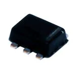
SOT-563 Package: 1.60 × 1.60 × 0.6 mm
Trip Point Accuracy:
– ±0.2°C (Typical) from –40°C to 125°C
Push-Pull Output
Selectable Hysteresis: 1/2/5/10°C
Supply Voltage Range: 1.4 V to 3.6 V
These devices require no additional components for
operation; each can function independent of
microprocessors or microcontrollers.
There are seven trip points available see Device
Options. Trip points can be programmed at the
factory to any desired temperature. For applications
that require different values, contact your local TI
representative.
2 Applications
•
•
•
•
•
Battery Charging
Battery Thermal Protection
Consumer Electronics
Enterprise
Telecom
The OUT pin is a push-pull, active-high output. When
the measured temperature is beyond the trip point
range, and the Set Output High (SOH) pin is low, the
OUT pin is high. The SOH pin is an input pin with an
internal pulldown resistor. When the SOH pin is
forced high, the OUT pin goes high regardless of the
measured temperature.
Device Information(1)
PART NUMBER
TMP303
PACKAGE
SOT-563 (6)
BODY SIZE (NOM)
1.60 mm × 1.20 mm
(1) For all available packages, see the orderable addendum at
the end of the data sheet.
TMP303 Functional Block Diagram
Typical Trip Threshold Accuracy at -20°C to 125°C
1.4V to 3.6V
40
VS
35
DS
ADC
OUT
HYSTSET0
HYSTSET1
Hysteresis
Logic
Trip Point
Logic
100kW
Population
30
Temperature
Sensor
25
20
15
10
5
GND
SOH
-1.0
-0.9
-0.8
-0.7
-0.6
-0.5
-0.4
-0.3
-0.2
-0.1
0
0.1
0.2
0.3
0.4
0.5
0.6
0.7
0.8
0.9
1.0
0
Temperature Accuracy (qC)
D003
1
An IMPORTANT NOTICE at the end of this data sheet addresses availability, warranty, changes, use in safety-critical applications,
intellectual property matters and other important disclaimers. PRODUCTION DATA.
�TMP303
SBOS486I – JULY 2009 – REVISED DECEMBER 2018
www.ti.com
Table of Contents
1
2
3
4
5
6
7
8
Features ..................................................................
Applications ...........................................................
Description .............................................................
Revision History.....................................................
Device Options.......................................................
Pin Configuration and Functions .........................
Specifications.........................................................
1
1
1
2
3
3
4
7.1
7.2
7.3
7.4
7.5
7.6
4
4
4
4
5
6
Absolute Maximum Ratings ......................................
ESD Ratings..............................................................
Recommended Operating Conditions.......................
Thermal Information ..................................................
Electrical Characteristics...........................................
Typical Characteristics ..............................................
Detailed Description .............................................. 8
8.1 Overview ................................................................... 8
8.2 Functional Block Diagram ......................................... 8
8.3 Feature Description................................................... 9
8.4 Device Functional Modes........................................ 11
9
Application and Implementation ........................ 12
9.1 Application Information............................................ 12
9.2 Typical Applications ................................................ 12
10 Power Supply Recommendations ..................... 16
11 Layout................................................................... 16
11.1 Layout Guidelines ................................................. 16
11.2 Layout Example .................................................... 16
12 Device and Documentation Support ................. 17
12.1
12.2
12.3
12.4
12.5
Receiving Notification of Documentation Updates
Community Resources..........................................
Trademarks ...........................................................
Electrostatic Discharge Caution ............................
Glossary ................................................................
17
17
17
17
17
13 Mechanical, Packaging, and Orderable
Information ........................................................... 17
4 Revision History
NOTE: Page numbers for previous revisions may differ from page numbers in the current version.
Changes from Revision H (October 2018) to Revision I
Page
•
Changed input pin voltage maximum value in the Absolute Maximum Ratings table from: ((V+) + 0.5) and ≤ 4 to:
((VS) + 0.3) and ≤ 4 ............................................................................................................................................................... 4
•
Changed output pin voltage maximum value n the Absolute Maximum Ratings table from: ((V+) + 0.5) and ≤ 4 to:
((VS) + 0.3) and ≤ 4 ............................................................................................................................................................... 4
Changes from Revision F (February 2016) to Revision G
Page
•
Added TMP303E, TMP303F, TMP303G devices to data sheet............................................................................................. 1
•
Changed number of Device Options from 4 to 7 ................................................................................................................... 1
•
Changed Trip Point Accuracy in Electrical Characteristics from TA = -20 to 125°C to TA = 60 to 125°C .............................. 5
Changes from Revision E (October 2015) to Revision F
Page
•
Added cross reference to Device Option Table. ................................................................................................................... 1
•
Added new image for Trip Threshold Accuracy .................................................................................................................... 1
•
Added Trip Points covering range -20 to 125°C .................................................................................................................... 5
•
Added Trip Accuracy Error vs Temperature graph. ............................................................................................................... 6
Changes from Revision D (September 2015) to Revision E
•
Changed I/O value of HYSTSET1 row in Pin Functions table .................................................................................................. 3
Changes from Revision C (September 2015) to Revision D
•
2
Page
Page
Consolidated part number to a generic TMP303.................................................................................................................... 1
Submit Documentation Feedback
Copyright © 2009–2018, Texas Instruments Incorporated
Product Folder Links: TMP303
�TMP303
www.ti.com
SBOS486I – JULY 2009 – REVISED DECEMBER 2018
Changes from Revision B (January 2011) to Revision C
•
Page
Added ESD Ratings table, Feature Description section, Device Functional Modes section, Application and
Implementation section, Power Supply Recommendations section, Layout section, Device and Documentation
Support section, and Mechanical, Packaging, and Orderable Information section ............................................................... 1
Changes from Revision A (September 2009) to Revision B
•
Page
Added TMP303B device to data sheet................................................................................................................................... 1
5 Device Options
(1)
DEVICE
TRIP POINTS (°C)
TMP303A
TL = 0, TH = 60 (1)
TMP303B
TL = 0, TH = 55 (1)
TMP303C
TL = -20, TH = 60 (1)
TMP303D
TL = -15, TH = 125 (1)
TMP303E
TL = 0, TH = 70 (1)
TMP303F
TL = 0, TH = 80 (1)
TMP303G
TL = 0, TH = 90 (1)
Contact a TI representative for other trip points.
6 Pin Configuration and Functions
DRL Package
6-Pin SOT-563
Top View
HYSTSET0 1
6
HYSTSET1
GND
2
5
VS
OUT
3
4
SOH
Pin Functions
PIN
NAME
NO.
I/O
HYSTSET0
1
Digital Input
GND
2
OUT
3
SOH
4
Digital Input
VS
5
Power
Supply
HYSTSET1
6
Digital Input
Ground
DESCRIPTION
This pin is used to set the amount of thermal hysteresis.
Ground
Digital Output Active high, push-pull output pin. Does not require a pullup resistor to VS.
Set output high (SOH) pin. If the SOH pin is pulled high, the TMP303 forces the output high.
If the SOH pin is grounded or left floating, this pin has no effect on the behavior of the
TMP303.
Power supply
This pin is used to set the amount of thermal hysteresis.
Submit Documentation Feedback
Copyright © 2009–2018, Texas Instruments Incorporated
Product Folder Links: TMP303
3
�TMP303
SBOS486I – JULY 2009 – REVISED DECEMBER 2018
www.ti.com
7 Specifications
7.1 Absolute Maximum Ratings
over operating free-air temperature range (unless otherwise noted) (1)
MIN
MAX
UNIT
4
V
Supply Voltage, VS – GND
Input Pins, Voltage
SOH, HYSTSET1, HYSTSET0
–0.5
((VS) + 0.3)
and ≤ 4
V
Output Pin, Voltage
OUT
–0.5
((VS) + 0.3)
and ≤ 4
V
Output Pin, Current
OUT
–55
8
mA
Operating Temperature
130
°C
Junction Temperature, TJ max
150
°C
150
°C
Storage Temperature, Tstg
(1)
–60
Stresses beyond those listed under Absolute Maximum Ratings may cause permanent damage to the device. These are stress ratings
only, which do not imply functional operation of the device at these or any other conditions beyond those indicated under Recommended
Operating Conditions. Exposure to absolute-maximum-rated conditions for extended periods may affect device reliability.
7.2 ESD Ratings
VALUE
Human-body model (HBM), per ANSI/ESDA/JEDEC JS-001
V(ESD)
(1)
(2)
Electrostatic discharge
(1)
UNIT
±2000
Charged-device model (CDM), per JEDEC specification JESD22C101 (2)
±1000
Machine model (MM)
±200
V
JEDEC document JEP155 states that 500-V HBM allows safe manufacturing with a standard ESD control process.
JEDEC document JEP157 states that 250-V CDM allows safe manufacturing with a standard ESD control process.
7.3 Recommended Operating Conditions
over operating free-air temperature range (unless otherwise noted)
MIN
NOM
MAX
UNIT
VS
Power Supply Voltage
1.4
3.6
V
TA
Specified Temperature Range
–40
125
°C
7.4 Thermal Information
TMP303
THERMAL METRIC
(1)
DRL (SOT-563)
UNIT
6 PINS
RθJA
Junction-to-ambient thermal resistance
210.3
°C/W
RθJC(top)
Junction-to-case (top) thermal resistance
105.0
°C/W
RθJB
Junction-to-board thermal resistance
87.5
°C/W
ψJT
Junction-to-top characterization parameter
6.1
°C/W
ψJB
Junction-to-board characterization parameter
87.0
°C/W
RθJC(bot)
Junction-to-case (bottom) thermal resistance
N/A
°C/W
(1)
4
For more information about traditional and new thermal metrics, see the Semiconductor and IC Package Thermal Metrics application
report, SPRA953.
Submit Documentation Feedback
Copyright © 2009–2018, Texas Instruments Incorporated
Product Folder Links: TMP303
�TMP303
www.ti.com
SBOS486I – JULY 2009 – REVISED DECEMBER 2018
7.5 Electrical Characteristics
At TA = –40°C to 125°C and VS = 1.4 V to 3.6 V, unless otherwise noted. (1)
PARAMETER
CONDITIONS
MIN
TYP
MAX
UNIT
TEMPERATURE MEASUREMENT
TL, TH Trip Point Accuracy (2)
TA = 55°C to 60°C, VS = 3.3 V
±0.2
±1
TA = -20 to 60°C, VS = 1.4 V to 3.6 V
±0.2
±1.5
TA = 60 to 125°C, VS = 1.4 V to 3.6 V
±0.2
±2.0
vs Supply
Hysteresis
±0.1
See Bit Setting vs Hysteresis Window
1
°C
°C/V
10
°C
HYSTERESIS SET INPUT
Input Logic Levels
Input Current
VIH
0.7 × VS
3.6
VIL
–0.5
0.3 × VS
IIN
0 < VIN < 3.6 V
V
1
μA
120
kΩ
SOH INPUT
Pulldown Resistor Value
Input Logic Levels
80
100
VIH
0.7 × VS
3.6
VIL
–0.5
0.3 × VS
Input Current
VIN = 3.6 V
V
36
μA
OUTPUT
VOH
Output Logic Levels
VOL
VS > 2 V, IOH = 0.5 mA
VS – 0.4
VS < 2 V, IOH = 0.5 mA
VS
VS – 0.2 × (VS)
VS
VS > 2 V, IOL = 1 mA
0
0.4
VS < 2 V, IOL = 1 mA
0
0.2 × VS
1.4
3.6
V
28
35
ms
3.5
5
4
8
V
POWER SUPPLY
Specified Supply
Voltage Range
VS
Power-up Start-up
Time
Quiescent Current
VS > 1.4 V
IQ
20
TA = –55°C to 60°C
TA = –40°C to 125°C
μA
TEMPERATURE RANGE
Specified Range
–40
125
°C
Operating Range
–55
130
°C
(1)
(2)
100% of all units are production tested at TA = 25°C. Over temperature specifications are specified by design.
TL, TH are device-specific. For example, TMP303A TL = 0°C, TH = 60°C; TMP303B TL = 0°C, TH = 55°C; TMP303C TL = –20°C, TH =
60°C; TMP303D TL = –15°C, TH = 125°C; TMP303E TL = 0°C, TH = 70°C; TMP303F TL = 0°C, TH = 80°C; TMP303G TL = 0°C, TH =
90°C
Submit Documentation Feedback
Copyright © 2009–2018, Texas Instruments Incorporated
Product Folder Links: TMP303
5
�TMP303
SBOS486I – JULY 2009 – REVISED DECEMBER 2018
www.ti.com
7.6 Typical Characteristics
At VS = 3.3 V and TA = 25°C, unless otherwise noted.
1
10
30 Units
9
Quiescent Current (mA)
0.75
Trip Accuracy (qC)
0.5
0.25
0
-0.25
-0.5
8
VS = 3.6V
7
6
5
4
3
VS = 1.4V
2
VS = 3.3V
1
-0.75
0
-1
-20
-60
0
20
40
60
80
Temperature (qC)
100
-40 -20
0
120
20
40
60
80
100 120 140
Temperature (°C)
D001
Figure 2. Quiescent Current vs Temperature
Figure 1. Trip Accuracy Error vs Temperature
100
120
90
80
Temperature (°C)
Temperature (°C)
100
80
60
40
70
60
50
40
30
20
20
10
0
0
0
5
10
15
20
25
0
30
20
40
Time (s)
60
80
100 120 140 160 180 200
Time (s)
Figure 3. Temperature Step Response in Perfluorinated
Fluid at 100°C vs Time
Figure 4. Thermal Step Response in Air at 100°C vs Time
40
35
OUT
Voltage (2V/div)
Population
30
25
20
15
VS
10
5
Time (8ms/div)
-1.0
-0.9
-0.8
-0.7
-0.6
-0.5
-0.4
-0.3
-0.2
-0.1
0
0.1
0.2
0.3
0.4
0.5
0.6
0.7
0.8
0.9
1.0
0
Temperature Accuracy (qC)
D003
Figure 5. Trip Threshold Accuracy at -20°C to 125°C
6
Figure 6. Power-Up and Power-Down Transient Response
Submit Documentation Feedback
Copyright © 2009–2018, Texas Instruments Incorporated
Product Folder Links: TMP303
�TMP303
www.ti.com
SBOS486I – JULY 2009 – REVISED DECEMBER 2018
Typical Characteristics (continued)
At VS = 3.3 V and TA = 25°C, unless otherwise noted.
300
250
OUT
200
VOL (mV)
Voltage (2V/div)
VS = 1.4V
IOL = 2mA
150
100
VS
50
0
-75
Time (10ms/div)
-50
-25
0
25
50
75
100
125
150
Temperature (°C)
Figure 7. Power-Up, Trip, and Power-Down Response
Figure 8. Output Logic Level Low vs Temperature
300
250
VS = 1.4V
IOH = 1mA
DVOH (mV)
200
150
100
50
0
-75
-50
-25
0
25
50
75
100
125
150
Temperature (°C)
Figure 9. Output Logic Level High vs Temperature
Submit Documentation Feedback
Copyright © 2009–2018, Texas Instruments Incorporated
Product Folder Links: TMP303
7
�TMP303
SBOS486I – JULY 2009 – REVISED DECEMBER 2018
www.ti.com
8 Detailed Description
8.1 Overview
The TMP303 devices are temperature switches used in battery-powered applications that require accurate
monitoring of a very specific temperature range from 0°C to 60°C (TMP303A), 0°C to 55°C (TMP303B), –20°C to
60°C (TMP303C), –15°C to 125°C (TMP303D), 0°C to 70°C (TMP303E), 0°C to 80°C (TMP303F) or 0°C to 90°C
(TMP303G). This functionality is accomplished through the preset trip window and two hysteresis bits, HYSTSET0
and HYSTSET1. The preset trip window temperature thresholds are configured at the factory; for other trip points,
contact a TI representative. Table 1 summarizes the bit setting versus hysteresis temperature window.
Table 1. Bit Setting vs Hysteresis Window
HYSTSET1
HYSTSET0
HYSTERESIS
GND
GND
1°C
GND
VS
2°C
VS
GND
5°C
VS
VS
10°C
8.2 Functional Block Diagram
1.4V to 3.6V
VS
Temperature
Sensor
DS
ADC
OUT
HYSTSET0
HYSTSET1
Hysteresis
Logic
Trip Point
Logic
100kW
GND
8
Submit Documentation Feedback
SOH
Copyright © 2009–2018, Texas Instruments Incorporated
Product Folder Links: TMP303
�TMP303
www.ti.com
SBOS486I – JULY 2009 – REVISED DECEMBER 2018
8.3 Feature Description
8.3.1 HYSTSET0, HYSTSET1 and SOH Functionality
The TMP303A temperature trip window resides within the range of 0°C to 60°C, the TMP303B within 0°C to
55°C, the TMP303C within –20°C to 60°C, the TMP303D within –15°C to 125°C, the TMP303E within 0°C to
70°C, the TMP303F within 0°C to 80°C, and the TMP303G within 0°C to 90°C. When any of these trip thresholds
is crossed, the output (OUT) changes state from low to high. OUT does not return to its original low state until
the temperature crosses the hysteresis threshold and returns within the range of the temperature trip window.
As an example, if the TMP303A is configured with a 10°C hysteresis window (that is, HYSTSET0 = HYSTSET1 =
VS), the output does not return to its low state until the temperature either crosses (TL + hysteresis) = 10°C or
(TH – hysteresis) = 50°C. The Set Output High (SOH) pin is intended to add test functionality to verify the
connectivity of the output (OUT) pin to the system controller or other temperature response system. The SOH pin
is internally pulled down to ground with a 100-kΩ resistor. If the SOH pin is grounded or left floating, it has no
effect on the behavior of the TMP303A. If the SOH pin is pulled high, the TMP303A immediately forces the
output high, regardless of temperature.
NOTE
This response occurs even if the temperature falls within the 0°C to 60°C temperature
window.
Figure 10 shows this design in graphical form.
TH = 60°C
50°C
Measured
Temperature
10°C
5°C
TL = 0°C
Changes hysteresis
from 10°C to 5°C
HYSTSET1
HYSTSET0
Forces OUT pin high
regardless of temperature
SOH
OUT
Time
Figure 10. TMP303A Output Transfer Curves With Hysteresis Change from 10°C to 5°C and SOH
Functionality
Submit Documentation Feedback
Copyright © 2009–2018, Texas Instruments Incorporated
Product Folder Links: TMP303
9
�TMP303
SBOS486I – JULY 2009 – REVISED DECEMBER 2018
www.ti.com
Feature Description (continued)
8.3.2 TMP303 Power Up and Timing
At device power up, the TMP303 exerts OUT = high, and typically requires 26 ms to return to a low state only if
the temperature falls within the hysteresis window set by HYSTSET0 and HYSTSET1.
The tolerance of the thermal response time is largely a result of the differences in conversion time, which varies
from 20 ms to 35 ms; likewise, this conversion does not take place after a power cycle until the supply voltage
has reached a level of at least 1.4 V. This sequence is illustrated in Figure 11.
60°C
60°C
3.3V
Temperature
1.4V
VS
1.4V
0°C
0°C
50
100
OUT = High
At Power-on
1
HYSTSET0 = High
HYSTSET1 = High
SOH = Low
OUT = High
After Conversion
Conversion
Time
Dt = 35ms (max)
0
0
50
100
0
OUT Logic State
0
OUT Logic State
3.3V
Temperature
Power Supply (V)
Power Supply (V)
VS
Ambient Temperature (°C)
50°C
Ambient Temperature (°C)
50°C
50
100
OUT = High
At Power-on
1
HYSTSET0 = High
HYSTSET1 = High
SOH = Low
Conversion
Time
Dt = 35ms (max)
OUT = Low
After Conversion
0
0
Time (ms)
50
100
Time (ms)
(a)
(b)
Figure 11. TMP303A Start-Up Delay vs Output Voltage (HYSTSET0 = HYSTSET1 = VS)
After the TMP303 powers up, all successive thermal response results for the device are achieved in a time frame
of 0.985 s to 1 s. This period is the minimum time frame required for the push-pull output (OUT) to change its
state from high to low (or conversely) when the device is active.
10
Submit Documentation Feedback
Copyright © 2009–2018, Texas Instruments Incorporated
Product Folder Links: TMP303
�TMP303
www.ti.com
SBOS486I – JULY 2009 – REVISED DECEMBER 2018
Feature Description (continued)
A maximum low output voltage is defined as a voltage level equivalent to (0.2 × VS); likewise, a minimum highoutput voltage is defined as (0.8 × VS). The timing associated with start-up time and conversion is shown in
Figure 12.
70
60
Temperature (°C)
50
40
30
20
10
0
0.01
0.1
1.0
10
1.0
10
OUT
Time (sec)
1
0
0.01
0.1
Time (sec)
Figure 12. TMP303A Start-Up and Conversion Timing (HYSTSET0 = HYSTSET1 = VS)
8.4 Device Functional Modes
The TMP303 family of devices has a single functional mode. Normal operation for the TMP303 family of devices
occurs when the power-supply voltage applied between the VS pin and GND is within the specified operating
range of 1.4 to 3.6 V.The temperature threshold is configured at the factory and the hysteresis is selected by
connecting the HYSTSET0 and HYSTSET1 pins to either the GND or Vs pins (see Table 1).
Submit Documentation Feedback
Copyright © 2009–2018, Texas Instruments Incorporated
Product Folder Links: TMP303
11
�TMP303
SBOS486I – JULY 2009 – REVISED DECEMBER 2018
www.ti.com
9 Application and Implementation
NOTE
Information in the following applications sections is not part of the TI component
specification, and TI does not warrant its accuracy or completeness. TI’s customers are
responsible for determining suitability of components for their purposes. Customers should
validate and test their design implementation to confirm system functionality.
9.1 Application Information
The TMP303 family of devices is simple to configure. The TMP303 contains an active high, push-pull output
stage and does not require a pullup resistor to VS for proper operation. The only external component that the
device requires is a bypass capacitor. TI strongly recommends using a 0.1-µF capacitor, placed as close as
possible to the supply pin.
9.2 Typical Applications
9.2.1 TMP303 Typical Configuration
Figure 13 shows the typical circuit configuration for the TMP303 family of devices. These devices have
preprogrammed trip-points. Select the TMP303 device that meets the application temperature trip requirement.
TMP303
HYSTSET0
GND
HYSTSET1
VS
0.1 F
OUTPUT
OUT
SOH
VS
1.4 V to 3.6 V
Figure 13. TMP303 Typical Application Configuration Schematic
9.2.1.1 Design Requirements
The TMP303 is a temperature switch commonly used to signal a microprocessor in the event of an over or under
temperature condition. The temperature that the TMP303 issues a output is determined by the device preset trip
window. The TMP303 issues an output when the temperature threshold is exceeded. To avoid the TMP303
signaling the microprocessor as soon as the temperature drops below the temperature threshold the TMP303
has a built-in hysteresis. The amount of hysteresis is determined by the hysteresis pins, HYSTSET0 and
HYSTSET1 . These pins are digital inputs and must be tied either high or low, according to Table 1.
9.2.1.2 Detailed Design Procedure
Select the appropriate TMP303 device that matches the application requirements; see the Device Options table
for different trip point ranges. Connect the HYSTSET0 and HYSTSET1 pins according to the application
requirements; see Table 1. In Figure 13 the TMP303 device is configured with a 1°C hysteresis window (that is,
HYSTSET0 = HYSTSET1 = GND). Place a 0.1-µF bypass capacitor close to the TMP303 device to reduce the noise
coupled from the power supply.
12
Submit Documentation Feedback
Copyright © 2009–2018, Texas Instruments Incorporated
Product Folder Links: TMP303
�TMP303
www.ti.com
SBOS486I – JULY 2009 – REVISED DECEMBER 2018
Typical Applications (continued)
9.2.1.3 Application Curves
Figure 14 and Figure 15 show the TMP303A power-on response with the ambient temperature (TA) less than
60°C and greater than 60°C respectively. TMP303B, TMP303C, TMP303D, TMP303E, TMP303F, and TMP303G
devices behave similarly with regards to power-on response with TA below or above the trip point.
Figure 15. TMP303A Power-On Response, TA Greater Than
60°C
Figure 14. TMP303A Power-On Response, TA Less Than
60°C
9.2.2 TMP303 With Switches
Figure 16 shows the most generic implementation of the TMP303 family of devices. Switches are shown
connecting the HYSTSET0 and HYSTSET1 pins to either VS or GND. The use of switches is not a requirement; the
switches are shown only to illustrate the various pin connection combinations. In practice, connecting the
HYSTSET0 and HYSTSET1 pins to ground or directly to the VS pin is sufficient and minimizes board space and
cost. If additional flexibility is desired, connections from the HYSTSET0 and HYSTSET1 pins can be made through
0-Ω resistors, which can be either populated or not, depending upon the desired connection.
TMP303
HYSTSET0
HYSTSET1
GND
VS
OUT
SOH
0.1 F
OUTPUT
VS
1.4 V to 3.6 V
Figure 16. TMP303 With Switches
Submit Documentation Feedback
Copyright © 2009–2018, Texas Instruments Incorporated
Product Folder Links: TMP303
13
�TMP303
SBOS486I – JULY 2009 – REVISED DECEMBER 2018
www.ti.com
Typical Applications (continued)
9.2.3 Simple Fan Controller
The circuit in Figure 17 senses system temperature and turns a cooling fan on when the sensor's temperature
exceeds a preselected value. The TMP303 device can be used directly to control the fan. The OUT pin is active
high, and it can be used directly to drive the DC fan. When temperature is within the temperature limits of the
system, the fan turns off, and when the temperature exceeds the trip-point, the fan turns on. In this example, the
TMP303A device is used and is configured with a 1°C hysteresis window (HYSTSET0 = HYSTSET1 = GND). The
TMP303A high trip-point is 60°C. When this trip-point temperature is exceeded, the output (OUT) changes state
from low to high. The output does not return to its low state until the temperature decreases below
(TH – hysteresis) = 59°C.
TMP303
HYSTSET0
12 V
GND
HYSTSET1
VS
0.1 F
OUT
SOH
VS
1.4 V to 3.6 V
OUTPUT
Figure 17. Simple Fan Controller
14
Submit Documentation Feedback
Copyright © 2009–2018, Texas Instruments Incorporated
Product Folder Links: TMP303
�TMP303
www.ti.com
SBOS486I – JULY 2009 – REVISED DECEMBER 2018
Typical Applications (continued)
9.2.4 Wireless Fixed Temperature Heat Detector
Heat detectors are needed in building automation. Conventional heat detectors need cables to supply power and
send the information back to a central system. Adding cables can be very costly and technically challenging in
old buildings, this leads to wireless battery operated heat detectors as preferred solutions. Running on battery
requires designing a very low power system for long haul. TMP303 can be used to design a low power heat
detector due to its very low quiescent current (5 µA maximum). The TMP303 device does not require any
additional components and can be interfaced with the MCU using only one GPIO. As an example, a wireless
transceiver with internal MCU can be used to monitor the TMP303 and communicate with a central system or
turn on an alarm in case of temperatures exceeding the trip-point. Figure 18 shows typical connections.
TMP303
HYSTSET0
VS
HYSTSET1
VS
VS
GND
+Coin Cell Battery
(3 V)
Wireless
MCU
0.1 F
OUT
GPIO
-
SOH
Figure 18. Wireless Fixed Temperature Heat Detector
Submit Documentation Feedback
Copyright © 2009–2018, Texas Instruments Incorporated
Product Folder Links: TMP303
15
�TMP303
SBOS486I – JULY 2009 – REVISED DECEMBER 2018
www.ti.com
10 Power Supply Recommendations
The TMP303 family of devices is designed to operate from a single power supply within the range of 1.4 V to
3.6 V. No specific power supply sequencing with respect to any of the input or output pins is required.
11 Layout
11.1 Layout Guidelines
Mount the TMP303 to a PCB as shown in Figure 19. For this example the HYSTSET0 and HYSTSET1 pins are
connected directly to ground. Connecting these pins to ground configures the device for 1°C hysteresis. The
SOH pin is grounded in this layout. Leaving this pin floating has no effect on the behavior of the TMP303.
•
•
Bypass the VS pin to ground with a low-ESR ceramic bypass capacitor. The typical recommended bypass
capacitance is a 0.1-μF ceramic capacitor with a X5R or X7R dielectric. The optimum placement is closest to
the VS and GND pins of the device. Take care in minimizing the loop area formed by the bypass-capacitor
connection, the VS pin, and the GND pin of the IC. Additional bypass capacitance can be added to
compensate for noisy or high-impedance power supplies.
The OUT pin is a push-pull, active-high output and does not require a pullup resistor to VS.
11.2 Layout Example
VIA to Power Ground Plane
0.1 µF
HYSTSET0
GND
HYSTSET1
TMP303
VS
Supply Voltage
OUT
SOH
Output
Ground Plane for
Thermal
Coupling to Heat
Source
Heat Source
Figure 19. PCB Layout Example
16
Submit Documentation Feedback
Copyright © 2009–2018, Texas Instruments Incorporated
Product Folder Links: TMP303
�TMP303
www.ti.com
SBOS486I – JULY 2009 – REVISED DECEMBER 2018
12 Device and Documentation Support
12.1 Receiving Notification of Documentation Updates
To receive notification of documentation updates, navigate to the device product folder on ti.com. In the upper
right corner, click on Alert me to register and receive a weekly digest of any product information that has
changed. For change details, review the revision history included in any revised document.
12.2 Community Resources
The following links connect to TI community resources. Linked contents are provided "AS IS" by the respective
contributors. They do not constitute TI specifications and do not necessarily reflect TI's views; see TI's Terms of
Use.
TI E2E™ Online Community TI's Engineer-to-Engineer (E2E) Community. Created to foster collaboration
among engineers. At e2e.ti.com, you can ask questions, share knowledge, explore ideas and help
solve problems with fellow engineers.
Design Support TI's Design Support Quickly find helpful E2E forums along with design support tools and
contact information for technical support.
12.3 Trademarks
E2E is a trademark of Texas Instruments.
All other trademarks are the property of their respective owners.
12.4 Electrostatic Discharge Caution
This integrated circuit can be damaged by ESD. Texas Instruments recommends that all integrated circuits be handled with
appropriate precautions. Failure to observe proper handling and installation procedures can cause damage.
ESD damage can range from subtle performance degradation to complete device failure. Precision integrated circuits may be more
susceptible to damage because very small parametric changes could cause the device not to meet its published specifications.
12.5 Glossary
SLYZ022 — TI Glossary.
This glossary lists and explains terms, acronyms, and definitions.
13 Mechanical, Packaging, and Orderable Information
The following pages include mechanical, packaging, and orderable information. This information is the most
current data available for the designated devices. This data is subject to change without notice and revision of
this document. For browser-based versions of this data sheet, refer to the left-hand navigation.
Submit Documentation Feedback
Copyright © 2009–2018, Texas Instruments Incorporated
Product Folder Links: TMP303
17
�PACKAGE OPTION ADDENDUM
www.ti.com
13-Aug-2022
PACKAGING INFORMATION
Orderable Device
Status
(1)
Package Type Package Pins Package
Drawing
Qty
Eco Plan
(2)
Lead finish/
Ball material
MSL Peak Temp
Op Temp (°C)
Device Marking
(3)
Samples
(4/5)
(6)
TMP303ADRLR
ACTIVE
SOT-5X3
DRL
6
4000
RoHS & Green NIPDAU | NIPDAUAG
Level-1-260C-UNLIM
-40 to 125
OCO
Samples
TMP303ADRLT
ACTIVE
SOT-5X3
DRL
6
250
RoHS & Green NIPDAU | NIPDAUAG
Level-1-260C-UNLIM
-40 to 125
OCO
Samples
TMP303BDRLR
ACTIVE
SOT-5X3
DRL
6
4000
RoHS & Green NIPDAU | NIPDAUAG
Level-1-260C-UNLIM
-40 to 125
QWM
Samples
TMP303BDRLT
ACTIVE
SOT-5X3
DRL
6
250
RoHS & Green NIPDAU | NIPDAUAG
Level-1-260C-UNLIM
-40 to 125
QWM
Samples
TMP303CDRLR
ACTIVE
SOT-5X3
DRL
6
4000
RoHS & Green
NIPDAU
Level-1-260C-UNLIM
-40 to 125
11U
Samples
TMP303CDRLT
ACTIVE
SOT-5X3
DRL
6
250
RoHS & Green
NIPDAU
Level-1-260C-UNLIM
-40 to 125
11U
Samples
TMP303DDRLR
ACTIVE
SOT-5X3
DRL
6
4000
RoHS & Green
NIPDAU
Level-1-260C-UNLIM
-40 to 125
(11U, 12Z)
Samples
TMP303DDRLT
ACTIVE
SOT-5X3
DRL
6
250
RoHS & Green
NIPDAU
Level-1-260C-UNLIM
-40 to 125
12Z
Samples
TMP303EDRLR
ACTIVE
SOT-5X3
DRL
6
4000
RoHS & Green
NIPDAU
Level-1-260C-UNLIM
-40 to 125
17Z
Samples
TMP303EDRLT
ACTIVE
SOT-5X3
DRL
6
250
RoHS & Green
NIPDAU
Level-1-260C-UNLIM
-40 to 125
17Z
Samples
TMP303FDRLR
ACTIVE
SOT-5X3
DRL
6
4000
RoHS & Green
NIPDAU
Level-1-260C-UNLIM
-40 to 125
18A
Samples
TMP303FDRLT
ACTIVE
SOT-5X3
DRL
6
250
RoHS & Green
NIPDAU
Level-1-260C-UNLIM
-40 to 125
18A
Samples
TMP303GDRLR
ACTIVE
SOT-5X3
DRL
6
4000
RoHS & Green
NIPDAU
Level-1-260C-UNLIM
-40 to 125
18B
Samples
TMP303GDRLT
ACTIVE
SOT-5X3
DRL
6
250
RoHS & Green
NIPDAU
Level-1-260C-UNLIM
-40 to 125
18B
Samples
(1)
The marketing status values are defined as follows:
ACTIVE: Product device recommended for new designs.
LIFEBUY: TI has announced that the device will be discontinued, and a lifetime-buy period is in effect.
NRND: Not recommended for new designs. Device is in production to support existing customers, but TI does not recommend using this part in a new design.
PREVIEW: Device has been announced but is not in production. Samples may or may not be available.
OBSOLETE: TI has discontinued the production of the device.
(2)
RoHS: TI defines "RoHS" to mean semiconductor products that are compliant with the current EU RoHS requirements for all 10 RoHS substances, including the requirement that RoHS substance
do not exceed 0.1% by weight in homogeneous materials. Where designed to be soldered at high temperatures, "RoHS" products are suitable for use in specified lead-free processes. TI may
reference these types of products as "Pb-Free".
Addendum-Page 1
�PACKAGE OPTION ADDENDUM
www.ti.com
13-Aug-2022
RoHS Exempt: TI defines "RoHS Exempt" to mean products that contain lead but are compliant with EU RoHS pursuant to a specific EU RoHS exemption.
Green: TI defines "Green" to mean the content of Chlorine (Cl) and Bromine (Br) based flame retardants meet JS709B low halogen requirements of


 工商网监
湘ICP备2023018690号
工商网监
湘ICP备2023018690号
