Product
Folder
Sample &
Buy
Technical
Documents
Tools &
Software
Support &
Community
TMS570LC4357
SPNS195C – FEBRUARY 2014 – REVISED JUNE 2016
TMS570LC4357 Hercules™ Microcontroller Based on the ARM® Cortex®-R Core
1 Device Overview
1.1
Features
1
• High-Performance Automotive-Grade
Microcontroller for Safety-Critical Applications
– Dual-Core Lockstep CPUs With ECC-Protected
Caches
– ECC on Flash and RAM Interfaces
– Built-In Self-Test (BIST) for CPU, High-End
Timers, and On-Chip RAMs
– Error Signaling Module (ESM) With Error Pin
– Voltage and Clock Monitoring
• ARM® Cortex® - R5F 32-Bit RISC CPU
– 1.66 DMIPS/MHz With 8-Stage Pipeline
– FPU With Single- and Double-Precision
– 16-Region Memory Protection Unit (MPU)
– 32KB of Instruction and 32KB of Data Caches
With ECC
– Open Architecture With Third-Party Support
• Operating Conditions
– Up to 300-MHz CPU Clock
– Core Supply Voltage (VCC): 1.14 to 1.32 V
– I/O Supply Voltage (VCCIO): 3.0 to 3.6 V
• Integrated Memory
– 4MB of Program Flash With ECC
– 512KB of RAM With ECC
– 128KB of Data Flash for Emulated EEPROM
With ECC
• 16-Bit External Memory Interface (EMIF)
• Hercules™ Common Platform Architecture
– Consistent Memory Map Across Family
– Real-Time Interrupt (RTI) Timer (OS Timer)
– Two 128-Channel Vectored Interrupt Modules
(VIMs) With ECC Protection on Vector Table
• VIM1 and VIM2 in Safety Lockstep Mode
– Two 2-Channel Cyclic Redundancy Checker
(CRC) Modules
• Direct Memory Access (DMA) Controller
– 32 Channels and 48 Peripheral Requests
– ECC Protection for Control Packet RAM
– DMA Accesses Protected by Dedicated MPU
• Frequency-Modulated Phase-Locked Loop
(FMPLL) With Built-In Slip Detector
• Separate Nonmodulating PLL
• IEEE 1149.1 JTAG, Boundary Scan, and ARM
CoreSight™ Components
• Advanced JTAG Security Module (AJSM)
• Trace and Calibration Capabilities
– ETM™, RTP, DMM, POM
• Multiple Communication Interfaces
– 10/100 Mbps Ethernet MAC (EMAC)
• IEEE 802.3 Compliant (3.3-V I/O Only)
• Supports MII, RMII, and MDIO
– FlexRay Controller With 2 Channels
• 8KB of Message RAM With ECC Protection
• Dedicated FlexRay Transfer Unit (FTU)
– Four CAN Controller (DCAN) Modules
• 64 Mailboxes, Each With ECC Protection
• Compliant to CAN Protocol Version 2.0B
– Two Inter-Integrated Circuit (I2C) Modules
– Five Multibuffered Serial Peripheral Interface
(MibSPI) Modules
• MibSPI1: 256 Words With ECC Protection
• Other MibSPIs: 128 Words With ECC
Protection
– Four UART (SCI) Interfaces, Two With Local
Interconnect Network (LIN 2.1) Interface
Support
• Two Next Generation High-End Timer (N2HET)
Modules
– 32 Programmable Channels Each
– 256-Word Instruction RAM With Parity
– Hardware Angle Generator for Each N2HET
– Dedicated High-End Timer Transfer Unit (HTU)
for Each N2HET
• Two 12-Bit Multibuffered Analog-to-Digital
Converter (MibADC) Modules
– MibADC1: 32 Channels Plus Control for up to
1024 Off-Chip Channels
– MibADC2: 25 Channels
– 16 Shared Channels
– 64 Result Buffers Each With Parity Protection
• Enhanced Timing Peripherals
– 7 Enhanced Pulse Width Modulator (ePWM)
Modules
– 6 Enhanced Capture (eCAP) Modules
– 2 Enhanced Quadrature Encoder Pulse (eQEP)
Modules
• Three On-Die Temperature Sensors
• Up to 145 Pins Available for General-Purpose I/O
(GPIO)
• 16 Dedicated GPIO Pins With External Interrupt
Capability
• Packages
– 337-Ball Grid Array (ZWT) [Green]
1
An IMPORTANT NOTICE at the end of this data sheet addresses availability, warranty, changes, use in safety-critical applications,
intellectual property matters and other important disclaimers. PRODUCTION DATA.
�TMS570LC4357
SPNS195C – FEBRUARY 2014 – REVISED JUNE 2016
1.2
•
•
•
•
2
www.ti.com
Applications
Braking Systems (Antilock Brake Systems and
Electronic Stability Control)
Electric Power Steering (EPS)
HEV and EV Inverter Systems
Battery-Management Systems
•
•
•
•
Active Driver Assistance Systems
Aerospace and Avionics
Railway Communications
Off-road Vehicles
Device Overview
Copyright © 2014–2016, Texas Instruments Incorporated
Submit Documentation Feedback
Product Folder Links: TMS570LC4357
�TMS570LC4357
www.ti.com
1.3
SPNS195C – FEBRUARY 2014 – REVISED JUNE 2016
Description
The TMS570LC4357 device is part of the Hercules TMS570 series of high-performance automotive-grade
ARM® Cortex®-R-based MCUs. Comprehensive documentation, tools, and software are available to
assist in the development of ISO 26262 and IEC 61508 functional safety applications. Start evaluating
today with the Hercules TMS570LC43x LaunchPad Development Kit. The TMS570LC4357 device has onchip diagnostic features including: dual CPUs in lockstep, Built-In Self-Test (BIST) logic for CPU, the
N2HET coprocessors, and for on-chip SRAMs; ECC protection on the L1 caches, L2 flash, and SRAM
memories. The device also supports ECC or parity protection on peripheral memories and loopback
capability on peripheral I/Os.
The TMS570LC4357 device integrates two ARM Cortex-R5F floating-point CPUs, operating in lockstep,
which offer an efficient 1.66 DMIPS/MHz, and can run up to 300 MHz providing up to 498 DMIPS. The
device supports the big-endian [BE32] format.
The TMS570LC4357 device has 4MB of integrated flash and 512KB of data RAM with single-bit error
correction and double-bit error detection. The flash memory on this device is a nonvolatile, electrically
erasable and programmable memory, implemented with a 64-bit-wide data bus interface. The flash
operates on a 3.3-V supply input (the same level as the I/O supply) for all read, program, and erase
operations. The SRAM supports read and write accesses in byte, halfword, and word modes.
The TMS570LC4357 device features peripherals for real-time control-based applications, including two
Next Generation High-End Timer (N2HET) timing coprocessors with up to 64 total I/O terminals.
The N2HET is an advanced intelligent timer that provides sophisticated timing functions for real-time
applications. The timer is software-controlled, with a specialized timer micromachine and an attached I/O
port. The N2HET can be used for pulse-width-modulated outputs, capture or compare inputs, or GPIO.
The N2HET is especially well suited for applications requiring multiple sensor information or drive
actuators with complex and accurate time pulses. The High-End Timer Transfer Unit (HTU) can perform
DMA-type transactions to transfer N2HET data to or from main memory. A Memory Protection Unit (MPU)
is built into the HTU.
The Enhanced Pulse Width Modulator (ePWM) module can generate complex pulse width waveforms with
minimal CPU overhead or intervention. The ePWM is easy to use and supports both high-side and lowside PWM and deadband generation. With integrated trip zone protection and synchronization with the onchip MibADC, the ePWM is ideal for digital motor control applications.
The Enhanced Capture (eCAP) module is essential in systems where the accurately timed capture of
external events is important. The eCAP can also be used to monitor the ePWM outputs or for simple PWM
generation when not needed for capture applications.
The Enhanced Quadrature Encoder Pulse (eQEP) module directly interfaces with a linear or rotary
incremental encoder to get position, direction, and speed information from a rotating machine as used in
high-performance motion and position-control systems.
The device has two 12-bit-resolution MibADCs with 41 total channels and 64 words of parity-protected
buffer RAM. The MibADC channels can be converted individually or by group for special conversion
sequences. Sixteen channels are shared between the two MibADCs. Each MibADC supports three
separate groupings. Each sequence can be converted once when triggered or configured for continuous
conversion mode. The MibADC has a 10-bit mode for use when compatibility with older devices or faster
conversion time is desired. One of the channels in MibADC1 and two of the channels in MibADC2 can be
used to convert temperature measurements from the three on-chip temperature sensors.
The device has multiple communication interfaces: Five MibSPIs; four UART (SCI) interfaces, two with LIN
support; four CANs; two I2C modules;one Ethernet Controller; and one FlexRay controller. The SPI
provides a convenient method of serial interaction for high-speed communications between similar shiftregister type devices. The LIN supports the Local Interconnect standard (LIN 2.1) and can be used as a
UART in full-duplex mode using the standard Non-Return-to-Zero (NRZ) format. The DCAN supports the
CAN 2.0B protocol standard and uses a serial, multimaster communication protocol that efficiently
supports distributed real-time control with robust communication rates of up to 1 Mbps. The DCAN is ideal
Device Overview
Copyright © 2014–2016, Texas Instruments Incorporated
Submit Documentation Feedback
Product Folder Links: TMS570LC4357
3
�TMS570LC4357
SPNS195C – FEBRUARY 2014 – REVISED JUNE 2016
www.ti.com
for applications operating in noisy and harsh environments (for example, automotive and industrial fields)
that require reliable serial communication or multiplexed wiring. The FlexRay controller uses a dualchannel serial, fixed time base multimaster communication protocol with communication rates of 10 Mbps
per channel. A FlexRay Transfer Unit (FTU) enables autonomous transfers of FlexRay data to and from
main CPU memory. HTU transfers are protected by a dedicated, built-in MPU. The Ethernet module
supports MII, RMII, and Management Data I/O (MDIO) interfaces. The I2C module is a multimaster
communication module providing an interface between the microcontroller and an I2C-compatible device
through the I2C serial bus. The I2C module supports speeds of 100 and 400 kbps.
The Frequency-Modulated Phase-Locked Loop (FMPLL) clock module multiplies the external frequency
reference to a higher frequency for internal use. The Global Clock Module (GCM) manages the mapping
between the available clock sources and the internal device clock domains.
The device also has two External Clock Prescaler (ECP) modules. When enabled, the ECPs output a
continuous external clock on the ECLK1 and ECLK2 balls. The ECLK frequency is a user-programmable
ratio of the peripheral interface clock (VCLK) frequency. This low-frequency output can be monitored
externally as an indicator of the device operating frequency.
The Direct Memory Access (DMA) controller has 32 channels, 48 peripheral requests, and ECC protection
on its memory. An MPU is built into the DMA to protect memory against erroneous transfers.
The Error Signaling Module (ESM) monitors on-chip device errors and determines whether an interrupt or
external Error pin/ball (nERROR) is triggered when a fault is detected. The nERROR signal can be
monitored externally as an indicator of a fault condition in the microcontroller.
The External Memory Interface (EMIF) provides a memory extension to asynchronous and synchronous
memories or other slave devices.
A Parameter Overlay Module (POM) is included to enhance the debugging capabilities of application code.
The POM can reroute flash accesses to internal RAM or to the EMIF, thus avoiding the reprogramming
steps necessary for parameter updates in flash. This capability is particularly helpful during real-time
system calibration cycles.
Several interfaces are implemented to enhance the debugging capabilities of application code. In addition
to the built-in ARM Cortex-R5F CoreSight debug features, the Embedded Cross Trigger (ECT) supports
the interaction and synchronization of multiple triggering events within the SoC. An External Trace
Macrocell (ETM) provides instruction and data trace of program execution. For instrumentation purposes,
a RAM Trace Port (RTP) module is implemented to support high-speed tracing of RAM and peripheral
accesses by the CPU or any other master. A Data Modification Module (DMM) gives the ability to write
external data into the device memory. Both the RTP and DMM have no or minimal impact on the program
execution time of the application code.
With integrated safety features and a wide choice of communication and control peripherals, the
TMS570LC4357 device is an ideal solution for high-performance real-time control applications with safetycritical requirements.
Device Information (1)
PART NUMBER
TMS570LC4357ZWT
(1)
4
PACKAGE
BODY SIZE
NFBGA (337)
16.00 mm × 16.00 mm
For more information on these devices, see Section 10, Mechanical Packaging and Orderable
Information.
Device Overview
Copyright © 2014–2016, Texas Instruments Incorporated
Submit Documentation Feedback
Product Folder Links: TMS570LC4357
�TMS570LC4357
www.ti.com
1.4
SPNS195C – FEBRUARY 2014 – REVISED JUNE 2016
Functional Block Diagram
DMA
POM
512KB
SRAM
4MB Flash
w/
&
ECC
HTU1
FTU
EMIF
PCR2
EMIF_nWAIT
EMIF_CLK
EMIF_CKE
EMIF_nCS[4:2]
EMIF_ADDR[21:0]
EMIF_nCS[0]
EMIF_DATA [15:0]
EMIF_BA[1:0]
EMIF_nDQM[1:0]
EMIF_nOE
EMIF_nWE
EMIF_nRAS
EMIF_nCAS
EMIF_nRW
PMM
EPC
SYS
MII
CCMR5F
Lockstep
VIMs
eQEP
1,2
eQEPxA
eQEPxB
eQEPxS
eQEPxI
eCAP
1..6
eCAP[6:1]
ePWM
1..7
nTZ[3:1]
SYNCO
SYNCI
ePWMxA
ePWMxB
RTI
#5
DCC1
#3
#4
#6
STC1
STC2
nPORRST
nRST
ECLK[2:1]
SYS
ESM
nERROR
DCAN4
CAN4_RX
CAN4_TX
MibSPI1
MibSPI2
MibSPI3
MibSPI4
MibSPI5
FlexRay
FRAY_RX1
FRAY_TX1
FRAY_TXEN1
FRAY_RX2
FRAY_TX2
FRAY_TXEN2
GIOA[7:0]
GIO
GIOB[7:0]
N2HET2[31:0]
N2HET2
N2HET2_PIN_nDIS
N2HET1[31:0]
N2HET1
N2HET1_PIN_nDIS
AD1IN[23:16]/
AD2IN[7:0]
AD2IN[24:16]
AD2EVT
VCCAD
VSSAD
ADREFHI
ADREFLO
MibADC 2
CRC
1,2
DCAN3
DCAN2
MDCLK
MDIO
MII_RXD[3:0]
MII_RXER
MII_TXD[3:0]
MII_TXEN
MII_TXCLK
MII_RXCLK
MII_CRS
MII_RXDV
MII_COL
MDIO
SCM
#2
AD1IN[15:8]/
AD2IN[15:8]
NMPU
CAN1_RX
CAN1_TX
CAN2_RX
CAN2_TX
CAN3_RX
CAN3_TX
DCAN1
EMAC Slaves
DCC2
AD1EXT_ENA
_
AD1EXT_SEL[4:0]
AD1EVT
AD1IN[7:0]
AD1IN[31:24]
HTU2
PCR 3
EMIF
Slave
IOMM
Core
MibADC 1
EMAC
Peripheral Interconnect Subsystem
Color Legend for
Power Domains
#1
TPIU
DMM
DAP
PCR1
always on
ETMDATA[31:0]
ETMTRACECTL
]
ETMTRACECLK
ETMTRACECLKIN
nTRST
TMS
TCK
RTCK
TDI
TDO
NMPU
CPU Interconnect Subsystem
Core/RAM
RTP
NMPU
Dual Cortex -R5F
CPUs in lockstep
128KB
Flash for
EEPROM
Emulation
w/ ECC
RTPnENA
RTPSYNC
RTPCLK
RTPDATA[15:0]
uSCU
32KB Icache
& Dcache w /
ECC
DMMnENA
DMMSYNC
DMMCLK
DMMDATA[15:0]
Figure 1-1 shows the functional block diagram of the device.
LIN1/
SCI1
LIN2/
SCI2
MIBSPI1_CLK
MIBSPI1_SIMO[1:0]
MIBSPI1_SOMI[1:0]
MIBSPI1_nCS[5:0]
MIBSPI1_nENA
MIBSPI2_CLK
MIBSPI2_SIMO
MIBSPI2_SOMI
MIBSPI2_nCS[1:0]
MIBSPI2_nENA
MIBSPI3_CLK
MIBSPI3_SIMO
MIBSPI3_SOMI
MIBSPI3_nCS[5:0]
MIBSPI3_nENA
MIBSPI4_CLK
MIBSPI4_SIMO
MIBSPI4_SOMI
MIBSPI4_nCS[5:0]
MIBSPI4_nENA
MIBSPI5_CLK
MIBSPI5_SIMO[3:0]
MIBSPI5_SOMI[3:0]
MIBSPI5_nCS[5:0]
MIBSPI5_nENA
LIN1_RX
LIN1_TX
LIN2_RX
LIN2_TX
SCI 3
SCI3_RX
SCI3_TX
SCI4
SCI4_RX
SCI4_TX
I2C1
I2C1_SDA
I2C1_SCL
I2C2
I2C2_SDA
I2C2_SCL
Copyright © 2016, Texas Instruments Incorporated
Figure 1-1. Functional Block Diagram
Device Overview
Copyright © 2014–2016, Texas Instruments Incorporated
Submit Documentation Feedback
Product Folder Links: TMS570LC4357
5
�TMS570LC4357
SPNS195C – FEBRUARY 2014 – REVISED JUNE 2016
www.ti.com
Table of Contents
1
2
3
4
Device Overview ......................................... 1
6.13
On-Chip SRAM Initialization and Testing .......... 105
1.1
Features .............................................. 1
6.14
External Memory Interface (EMIF) ................. 109
1.2
Applications ........................................... 2
6.15
Vectored Interrupt Manager ........................ 117
1.3
Description ............................................ 3
6.16
ECC Error Event Monitoring and Profiling ......... 121
1.4
Functional Block Diagram ............................ 5
6.17
DMA Controller..................................... 123
Revision History ......................................... 7
Device Comparison ..................................... 8
Terminal Configuration and Functions .............. 9
6.18
Real-Time Interrupt Module ........................ 127
6.19
Error Signaling Module............................. 129
6.20
Reset / Abort / Error Sources ...................... 134
4.1
6.21
Digital Windowed Watchdog ....................... 138
6.22
Debug Subsystem
ZWT BGA Package Ball-Map (337 Terminal Grid
Array) ................................................. 9
Terminal Functions .................................. 10
4.2
5
..........................................
Absolute Maximum Ratings .........................
ESD Ratings ........................................
Power-On Hours (POH) .............................
Device Recommended Operating Conditions.......
Specifications
5.1
5.2
5.3
5.4
5.5
5.9
5.10
6
Peripheral Information and Electrical
Specifications ......................................... 156
7.1
Enhanced Translator PWM Modules (ePWM) ..... 156
7.2
Enhanced Capture Modules (eCAP) ............... 161
55
56
7.3
7.4
Switching Characteristics over Recommended
Operating Conditions for Clock Domains ........... 57
Enhanced Quadrature Encoder (eQEP) ........... 164
12-bit Multibuffered Analog-to-Digital Converter
(MibADC)........................................... 166
7.5
General-Purpose Input/Output ..................... 179
57
7.6
Enhanced High-End Timer (N2HET)
59
7.7
FlexRay Interface .................................. 185
Input/Output Electrical Characteristics Over
Recommended Operating Conditions ............... 60
Thermal Resistance Characteristics for the BGA
Package (ZWT) ..................................... 61
7.8
Controller Area Network (DCAN) .................. 187
Timing and Switching Characteristics ............... 61
System Information and Electrical
Specifications ........................................... 64
6.1
Device Power Domains ............................. 64
6.2
Voltage Monitor Characteristics ..................... 65
6.3
Power Sequencing and Power-On Reset ........... 66
6.4
Warm Reset (nRST)................................. 68
6.5
................. 69
Clocks ............................................... 76
Clock Monitoring .................................... 87
Glitch Filters ......................................... 89
Device Memory Map ................................ 90
Flash Memory ...................................... 101
L2RAMW (Level 2 RAM Interface Module) ........ 104
ARM Cortex-R5F CPU Information
6.6
6.7
6.8
6.9
6.10
6.11
6.12
6
55
55
Wait States Required - L2 Memories
5.7
5.8
139
55
...............
Power Consumption Summary......................
5.6
7
.................................
ECC / Parity Protection for Accesses to Peripheral
RAMs .............................................. 104
..............
180
7.9
Local Interconnect Network Interface (LIN) ........ 188
7.10
Serial Communication Interface (SCI) ............. 189
7.11
7.12
Inter-Integrated Circuit (I2C) ....................... 190
Multibuffered / Standard Serial Peripheral
Interface ............................................ 193
7.13
Ethernet Media Access Controller ................. 207
8
Applications, Implementation, and Layout ...... 211
9
Device and Documentation Support .............. 212
8.1
TI Design or Reference Design .................... 211
9.1
Device Support..................................... 212
9.2
Documentation Support ............................ 214
9.3
Trademarks ........................................ 214
9.4
Electrostatic Discharge Caution
9.5
Glossary............................................ 214
9.6
Device Identification................................ 215
9.7
Module Certifications............................... 217
10 Mechanical Data
10.1
...................
......................................
214
223
Packaging Information ............................. 223
Table of Contents
Copyright © 2014–2016, Texas Instruments Incorporated
Submit Documentation Feedback
Product Folder Links: TMS570LC4357
�TMS570LC4357
www.ti.com
SPNS195C – FEBRUARY 2014 – REVISED JUNE 2016
2 Revision History
This data manual revision history highlights the technical changes made to the SPNS195B device-specific
data manual to make it an SPNS195C revision. These devices are now in the Production Data (PD) stage
of development.
Changes from January 31, 2016 to June 25, 2016 (from B Revision (January 2016) to C Revision)
•
•
•
•
•
•
•
•
•
•
•
•
•
•
•
Page
Global: Updated/Changed the product status from Product Preview to Production Data. .................................. 1
Table 6-13 (LPO Specifications): Updated/Changed LPO - HF oscillator, Untrimmed frequency TYP value from
"9.6" to "9" MHz ..................................................................................................................... 78
Section 6.9.3 (Special Consideration for CPU Access Errors Resulting in Imprecise Aborts): Add missing
subsection ............................................................................................................................ 96
Section 6.14.1 (External Memory Interface (EMIF), Features): Updated/Changed the EMIF asynchronous
memory maximum addressable size from "32KB" to "16MB" each ......................................................... 109
Section 6.14 (External Memory Interface (EMIF)): Added 32-bit access note using a 16-bit EMIF interface. ........ 109
Added "Commonly caused by ..." statement for clarification ................................................................. 131
Table 6-56 (ETMTRACECLK Timing): Restructured timing table formatting to standards............................... 149
Table 7-7, (eCAPx Clock Enable Control): Updated/Changed "ePWM" to "eCAP" in the MODULE INSTANCE
column............................................................................................................................... 162
Table 7-11, (eQEPx Clock Enable Control): Updated/Changed "ePWM" to "eQEP" in the MODULE INSTANCE
column............................................................................................................................... 164
Table 7-16 (MibADC1 Event Trigger Selection): Added lead-in paragraph referencing the able ....................... 166
(MibADC1 Event Trigger Hookup): NOTE: Added new paragraph ......................................................... 168
Table 7-17 (MibADC2 Event Trigger Selection): Added lead-in paragraph referencing the able ....................... 168
Section 7.4.2.3 (Controlling ADC1 and ADC2 Event Trigger Options Using SOC Output from ePWM Modules):
Updated/Changed the names of the four ePWM signals that event trigger the ADC .................................... 170
Table 7-22 (MibADC Operating Characteristics Over 3.0 V to 3.6 V Operating Conditions): Updated/Changed
the 10- and 12-bit mode formulas to be superscript power of 2 values .................................................... 175
Table 7-23 (MibADC Operating Characteristics Over 3.6 V to 5.25 V Operating Conditions): Updated/Changed
the 10- and 12-bit mode formulas to be superscript power of 2 values .................................................... 175
Revision History
Copyright © 2014–2016, Texas Instruments Incorporated
Submit Documentation Feedback
Product Folder Links: TMS570LC4357
7
�TMS570LC4357
SPNS195C – FEBRUARY 2014 – REVISED JUNE 2016
www.ti.com
3 Device Comparison
Table 3-1 lists the features of the TMS570LC4357 devices.
Table 3-1. TMS570LC4357 Device Comparison (1) (2)
FEATURES
DEVICES
TMS570LC4357ZWT (3)
Generic Part Number
Package
TMS570LS3137ZWT (3)
TMS570LS3135ZWT
TMS570LS1227ZWT (3)
337 BGA
337 BGA
337 BGA
337 BGA
ARM Cortex-R5F
ARM Cortex-R4F
ARM Cortex-R4F
ARM Cortex-R4F
Frequency (MHz)
300
180
180
180
Cache (KB)
32 I
32 D
–
–
–
Flash (KB)
4096
3072
3072
1280
RAM (KB)
512
256
256
192
Data Flash [EEPROM] (KB)
128
64
64
64
10/100
10/100
–
10/100
2-ch
2-ch
2-ch
2-ch
4
3
3
3
2 (41ch)
2 (24ch)
2 (24ch)
2 (24ch)
CPU
EMAC
FlexRay
CAN
MibADC
12-bit (Ch)
N2HET (Ch)
2 (64)
2 (44)
2 (44)
2 (44)
ePWM Channels
14
–
–
14
eCAP Channels
6
–
–
6
eQEP Channels
2
–
–
2
5 (4 x 6 + 2)
3 (6 + 6 + 4)
3 (6 + 6 + 4)
3 (6 + 6 + 4)
MibSPI (CS)
SPI (CS)
–
2 (2 + 1)
2 (2 + 1)
2 (2 + 1)
SCI (LIN)
4 (2 with LIN)
2 (1 with LIN)
2 (1 with LIN)
2 (1 with LIN)
2
1
1
1
168 (with 16 interrupt capable)
144 (with 16 interrupt capable)
144 (with 16 interrupt capable)
101 (with 16 interrupt capable)
I2C
GPIO (INT) (4)
EMIF
16-bit data
16-bit data
16-bit data
16-bit data
ETM (Trace)
32-bit
32-bit
32-bit
–
RTP/DMM
16/16
16/16
16/16
–
Operating
Temperature
–40ºC to 125ºC
–40ºC to 125ºC
–40ºC to 125ºC
–40ºC to 125ºC
Core Supply (V)
1.14 V – 1.32 V
1.14 V – 1.32 V
1.14 V – 1.32 V
1.14 V – 1.32 V
3.0 V – 3.6 V
3.0 V – 3.6 V
3.0 V – 3.6 V
3.0 V – 3.6 V
I/O Supply (V)
(1)
(2)
(3)
(4)
8
For additional device variants, see www.ti.com/tms570.
This table reflects the maximum configuration for each peripheral. Some functions are multiplexed and not all pins are available at the
same time.
Superset device
Total number of pins that can be used as general-purpose input or output when not used as part of a peripheral.
Device Comparison
Copyright © 2014–2016, Texas Instruments Incorporated
Submit Documentation Feedback
Product Folder Links: TMS570LC4357
�TMS570LC4357
www.ti.com
SPNS195C – FEBRUARY 2014 – REVISED JUNE 2016
4 Terminal Configuration and Functions
4.1
ZWT BGA Package Ball-Map (337 Terminal Grid Array)
A
B
C
D
E
F
G
H
J
K
L
MIBSPI5
NCS[0]
MIBSPI1
SIMO[0]
MIBSPI1
NENA
MIBSPI5
CLK
MIBSPI5
SIMO[0]
N2HET1
[28]
DMM_
DATA[0]
M
N
P
R
T
U
V
W
DCAN3RX
AD1EVT
AD1IN[15]
/
AD2IN[15]
AD1IN[22]
/
AD2IN[06]
AD1IN
[06]
AD1IN[11]
/
AD2IN[11]
AD2IN[24]
VSSAD
19
18
19
VSS
VSS
TMS
N2HET1
[10]
18
VSS
TCK
TDO
nTRST
N2HET1
[08]
MIBSPI1
CLK
MIBSPI1
SOMI[0]
MIBSPI5
NENA
MIBSPI5
SOMI[0]
N2HET1
[0]
DMM_
DATA[1]
DCAN3TX
AD1IN[24]
AD1IN[08]
/
AD2IN[08]
AD1IN[14]
/
AD2IN[14]
AD1IN[13]
/
AD2IN[13]
AD1IN
[04]
AD1IN
[02]
AD2IN[24]
17
TDI
nRST
EMIF_
ADDR[21]
EMIF_
nWE
MIBSPI5
SOMI[1]
DMM_
CLK
MIBSPI5
SIMO[3]
MIBSPI5
SIMO[2]
N2HET1
[31]
EMIF_
nCS[3]
EMIF_
nCS[2]
EMIF_
nCS[4]
EMIF_
nCS[0]
AD1IN[25]
AD1IN
[05]
AD1IN
[03]
AD1IN[10]
/
AD2IN[10]
AD1IN
[01]
AD1IN[09]
/
17
AD2IN[09]
16
RTCK
FRAY
TXEN1
EMIF_
ADDR[20]
EMIF_
BA[1]
MIBSPI5
SIMO[1]
DMM_
nENA
MIBSPI5
SOMI[3]
MIBSPI5
SOMI[2]
DMM_
SYNC
N2HET2
[08]
N2HET2
[09]
N2HET2
[10]
N2HET2
[11]
AD1IN[26]
AD1IN[23]
/
AD2IN[07]
AD1IN[12]
/
AD2IN[12]
AD1IN[19]
/
AD2IN[03]
ADREFLO
VSSAD
16
FRAYTX1
EMIF_
ADDR[19]
EMIF_
ADDR[18]
ETM
DATA[06]
ETM
DATA[05]
ETM
DATA[04]
ETM
DATA[03]
ETM
DATA[02]
ETM
ETM
ETM
ETM
DATA[16] / DATA[17] / DATA[18] / DATA[19] /
AD1IN[27]
EMIF_
EMIF_
EMIF_
EMIF_
DATA[0]
DATA[1]
DATA[2]
DATA[3]
AD1IN[28]
AD1IN[21]
/
AD2IN[05]
AD1IN[20]
/
AD2IN[04]
ADREFHI
VCCAD
15
VCCIO
VCCIO
VCC
VCCIO
AD1IN[29]
AD1IN[30]
AD1IN[18]
/
AD2IN[02]
AD1IN
[07]
AD1IN
[0]
14
VCCIO
ETM
DATA[01]
AD1IN[31]
AD1IN[17]
/
AD2IN[01]
AD1IN[16]
/
AD2IN[0]
AD2IN[16] 13
15 FRAYRX1
14
N2HET1
[26]
nERROR
EMIF_
ADDR[17]
EMIF_
ADDR[16]
ETM
DATA[07]
VCCIO
13
N2HET1
[17]
N2HET1
[19]
EMIF_
ADDR[15]
N2HET2
[04]
ETM
DATA[12] /
EMIF_BA[
0]
VCCIO
12
ECLK
N2HET1
[04]
EMIF_
ADDR[14]
N2HET2
[05]
ETM
DATA[13] /
EMIF_nOE
VCCIO
VSS
VSS
VCC
VSS
VSS
VCCIO
ETM
DATA[0]
MIBSPI5
NCS[3]
AD2IN[19]
AD2IN[18]
AD2IN[17] 12
11
N2HET1
[14]
N2HET1
[30]
EMIF_
ADDR[13]
N2HET2
[06]
ETM
DATA[14] /
EMIF_
nDQM[1]
VCCIO
VSS
VSS
VSS
VSS
VSS
VCCPLL
ETM
TRACE
CTL
AD2IN[20]
AD2IN[21]
AD2IN[22]
AD2IN[23] 11
ePWM1B
ETM
DATA[15] /
EMIF_
nDQM[0]
VCC
VCC
VSS
VSS
VSS
VCC
VCC
ETM
TRACE
CLKOUT
AD2EVT
MIBSPI1
NCS[4]
MIBSPI3
NCS[0]
GIOB[3]
10
ePWM1A
ETM
DATA[08] /
EMIF_
ADDR[5]
VCC
VSS
VSS
VSS
VSS
VSS
VCCIO
ETM
TRACE
CLKIN
MDCLK
MIBSPI1
NCS[5]
MIBSPI3
CLK
MIBSPI3
NENA
9
ETM
DATA[09] /
EMIF_
N2HET2[1]
EMIF_
ADDR[10]
ADDR[4]
VCCP
VSS
VSS
VCC
VSS
VSS
VCCIO
ETM
DATA[31] /
EMIF_
DATA[15]
N2HET2
[23]
MII_TXD
[0]
MIBSPI3
SOMI
MIBSPI3
SIMO
8
VCCIO
ETM
DATA[30] /
EMIF_
DATA[14]
N2HET2
[22]
MII_TX_
CLK
N2HET1
[09]
VCCIO
ETM
DATA[29] /
EMIF_
DATA[13]
N2HET2
[21]
MII_RX_
DV
N2HET1
[05]
MIBSPI5
NCS[2]
6
ETM
ETM
ETM
ETM
ETM
ETM
DATA[23] / DATA[24] / DATA[25] / DATA[26] / DATA[27] / DATA[28] /
EMIF_
EMIF_
EMIF_
EMIF_
EMIF_
EMIF_
DATA[7]
DATA[8]
DATA[9]
DATA[10] DATA[11] DATA[12]
N2HET2
[20]
MII_RX_
ER
MIBSPI3
NCS[1]
N2HET1
[02]
5
EMIF_
10 DCAN1TX DCAN1RX ADDR[12]
9
N2HET1
[27]
8 FRAYRX2
FRAY
TXEN2
FRAYTX2
EMIF_
ADDR[11]
7
LIN1RX
LIN1TX
EMIF_
ADDR[9]
N2HET2
[2]
ETM
DATA[10] /
EMIF_
ADDR[3]
VCCIO
6
GIOA[4]
MIBSPI5
NCS[1]
EMIF_
ADDR[8]
N2HET2
[0]
ETM
DATA[11] /
EMIF_
ADDR[2]
VCCIO
5
GIOA[0]
GIOA[5]
EMIF_
ADDR[7]
EMIF_
ADDR[1]
ETM
ETM
ETM
DATA[20] / DATA[21] / DATA[22] /
EMIF_
EMIF_
EMIF_
DATA[4]
DATA[6]
DATA[5]
4
N2HET1
[16]
N2HET1
[12]
EMIF_
ADDR[6]
EMIF_
ADDR[0]
MII_TXEN
MDIO
3
N2HET1
[29]
N2HET1
[22]
MIBSPI3
NCS[3]
N2HET2
[12]
N2HET1
[11]
2
VSS
MIBSPI3
NCS[2]
GIOA[1]
N2HET2
[13]
1
VSS
VSS
GIOA[2]
A
B
C
VCCIO
VCC
VCC
VCCIO
VCC
VCCIO
VCCIO
VCCIO
VCCIO
nPORRST 7
VCCIO
VCCIO
FLTP2
FLTP1
MII_TXD
[3]
N2HET1
[21]
N2HET1
[23]
N2HET2
[15]
N2HET2
[16]
N2HET2
[17]
N2HET2
[18]
N2HET2
[19]
EMIF_
nCAS
MII_
RXCLK
MII_RXD
[0]
MII_CRS
MII_COL
4
MIBSPI1
NCS[1]
MIBSPI1
NCS[2]
GIOA[6]
MIBSPI1
NCS[3]
EMIF_
CLK
EMIF_
CKE
N2HET1
[25]
N2HET2
[7]
EMIF_
nWAIT
EMIF_
nRAS
MII_RXD
[1]
MII_RXD
[2]
MII_RXD
[3]
N2HET1
[06]
3
N2HET2
[3]
GIOB[2]
GIOB[5]
DCAN2TX
GIOB[6]
GIOB[1]
KELVIN_
GND
GIOB[0]
N2HET1
[13]
N2HET1
[20]
MIBSPI1
NCS[0]
MII_TXD
[2]
TEST
N2HET1
[1]
VSS
2
N2HET2
[14]
GIOA[3]
GIOB[7]
GIOB[4]
DCAN2RX
N2HET1
[18]
OSCIN
OSCOUT
GIOA[7]
N2HET1
[15]
N2HET1
[24]
MII_TXD
[1]
N2HET1
[7]
NHET1
[03]
VSS
VSS
1
D
E
F
G
H
J
K
L
M
N
P
R
T
U
V
W
Figure 4-1. ZWT Package Pinout. Top View
Note: Balls can have multiplexed functions. See Section 4.2.2 for detailed information.
Terminal Configuration and Functions
Copyright © 2014–2016, Texas Instruments Incorporated
Submit Documentation Feedback
Product Folder Links: TMS570LC4357
9
�TMS570LC4357
SPNS195C – FEBRUARY 2014 – REVISED JUNE 2016
4.2
www.ti.com
Terminal Functions
Table 4-1 through Table 4-27 identify the external signal names, the associated terminal numbers along
with the mechanical package designator, the terminal type (Input, Output, I/O, Power, or Ground), whether
the terminal has any internal pullup/pulldown, whether the terminal can be configured as a GIO, and a
functional terminal description. The first signal name listed is the primary function for that terminal. The
signal name in Bold is the function being described. For information on how to select between different
multiplexed functions, see the Section 4.2.2, Multiplexing of this data manual along with the I/O
Multiplexing Module (IOMM) chapter in the Technical Reference Manual (TRM) (SPNU563).
NOTE
In the Terminal Functions tables below, the "Default Pull State" is the state of the pull applied
to the terminal while nPORRST is low and immediately after nPORRST goes High. The
default pull direction may change when software configures the pin for an alternate function.
The "Pull Type" is the type of pull asserted when the signal name in bold is enabled for the
given terminal by the IOMM control registers.
All I/O signals except nRST are configured as inputs while nPORRST is low and immediately
after nPORRST goes High. While nPORRST is low, the input buffers are disabled, and the
output buffers are disabled with the default pulls enabled.
All output-only signals have the output buffer disabled and the default pull enabled while
nPORRST is low, and are configured as outputs with the pulls disabled immediately after
nPORRST goes High.
10
Terminal Configuration and Functions
Copyright © 2014–2016, Texas Instruments Incorporated
Submit Documentation Feedback
Product Folder Links: TMS570LC4357
�TMS570LC4357
www.ti.com
4.2.1
SPNS195C – FEBRUARY 2014 – REVISED JUNE 2016
ZWT Package
4.2.1.1
Multibuffered Analog-to-Digital Converters (MibADC)
Table 4-1. ZWT Multibuffered Analog-to-Digital Converters (MibADC1, MibADC2)
TERMINAL
SIGNAL NAME
337
ZWT
SIGNAL
TYPE
DEFAULT
PULL STATE
PULL TYPE
OUTPUT
BUFFER
DRIVE
STRENGTH
DESCRIPTION
AD1EVT/MII_RX_ER/RMII_RX_ER/nTZ1_1
N19
I/O
Pulldown
Programmable, 20 µA
2mA ZD
AD1IN[0]
W14
Input
-
-
-
ADC1 event trigger input, or GIO
ADC1 Input
AD1IN[1]
V17
Input
-
-
-
ADC1 Input
AD1IN[2]
V18
Input
-
-
-
ADC1 Input
AD1IN[3]
T17
Input
-
-
-
ADC1 Input
AD1IN[4]
U18
Input
-
-
-
ADC1 Input
AD1IN[5]
R17
Input
-
-
-
ADC1 Input
AD1IN[6]
T19
Input
-
-
-
ADC1 Input
AD1IN[7]
V14
Input
-
-
-
ADC1 Input
AD1IN[8]/AD2IN[8]
P18
Input
-
-
-
ADC1/ADC2 shared Input
AD1IN[9]/AD2IN[9]
W17
Input
-
-
-
ADC1/ADC2 shared Input
AD1IN[10]/AD2IN[10]
U17
Input
-
-
-
ADC1/ADC2 shared Input
AD1IN[11]/AD2IN[11]
U19
Input
-
-
-
ADC1/ADC2 shared Input
AD1IN[12]/AD2IN[12]
T16
Input
-
-
-
ADC1/ADC2 shared Input
AD1IN[13]/AD2IN[13]
T18
Input
-
-
-
ADC1/ADC2 shared Input
AD1IN[14]/AD2IN[14]
R18
Input
-
-
-
ADC1/ADC2 shared Input
AD1IN[15]/AD2IN[15]
P19
Input
-
-
-
ADC1/ADC2 shared Input
AD1IN[16]/AD2IN[0]
V13
Input
-
-
-
ADC1/ADC2 shared Input
AD1IN[17]/AD2IN[1]
U13
Input
-
-
-
ADC1/ADC2 shared Input
AD1IN[18]/AD2IN[2]
U14
Input
-
-
-
ADC1/ADC2 shared Input
AD1IN[19]/AD2IN[3]
U16
Input
-
-
-
ADC1/ADC2 shared Input
AD1IN[20]/AD2IN[4]
U15
Input
-
-
-
ADC1/ADC2 shared Input
AD1IN[21]/AD2IN[5]
T15
Input
-
-
-
ADC1/ADC2 shared Input
AD1IN[22]/AD2IN[6]
R19
Input
-
-
-
ADC1/ADC2 shared Input
AD1IN[23]/AD2IN[7]
R16
Input
-
-
-
ADC1/ADC2 shared Input
AD1IN[24]
N18
Input
-
-
-
ADC1 Input
Terminal Configuration and Functions
Copyright © 2014–2016, Texas Instruments Incorporated
Submit Documentation Feedback
Product Folder Links: TMS570LC4357
11
�TMS570LC4357
SPNS195C – FEBRUARY 2014 – REVISED JUNE 2016
www.ti.com
Table 4-1. ZWT Multibuffered Analog-to-Digital Converters (MibADC1, MibADC2) (continued)
TERMINAL
SIGNAL NAME
337
ZWT
SIGNAL
TYPE
DEFAULT
PULL STATE
PULL TYPE
OUTPUT
BUFFER
DRIVE
STRENGTH
DESCRIPTION
AD1IN[25]
P17
Input
-
-
-
ADC1 Input
AD1IN[26]
P16
Input
-
-
-
ADC1 Input
AD1IN[27]
P15
Input
-
-
-
ADC1 Input
AD1IN[28]
R15
Input
-
-
-
ADC1 Input
AD1IN[29]
R14
Input
-
-
-
ADC1 Input
AD1IN[30]
T14
Input
-
-
-
ADC1 Input
AD1IN[31]
T13
Input
-
-
-
ADC1 Input(1)
AD2EVT
T10
MIBSPI3NCS[0]/AD2EVT/eQEP1I
V10(2)
I/O
Pulldown
Programmable, 20 µA
2mA ZD
AD2IN[16]
W13
Input
-
-
-
ADC2 Input
AD2IN[17]
W12
Input
-
-
-
ADC2 Input
AD2IN[18]
V12
Input
-
-
-
ADC2 Input
AD2IN[19]
U12
Input
-
-
-
ADC2 Input
AD2IN[20]
T11
Input
-
-
-
ADC2 Input
AD2IN[21]
U11
Input
-
-
-
ADC2 Input
AD2IN[22]
V11
Input
-
-
-
ADC2 Input
AD2IN[23]
W11
Input
-
-
-
ADC2 Input
AD2IN[24]
V19
AD2IN[24]
W18
Input
-
-
-
ADC2 Input
ADREFHI
V15(3)
Input
-
-
-
ADC high reference supply
ADREFLO
V16(3)
Input
-
-
-
ADC low reference supply
MIBSPI3SOMI/AD1EXT_ENA/ECAP2
V8
MIBSPI5SOMI[3]/DMM_DATA[15]/I2C2_SCL/AD1EXT_ENA
G16
Output
Pullup
20 µA
2mA ZD
External Mux ENA
MIBSPI3SIMO/AD1EXT_SEL[0]/ECAP3
W8
MIBSPI5SIMO[1]/DMM_DATA[9]/AD1EXT_SEL[0]
E16
Output
Pullup
20 µA
2mA ZD
External Mux Select 0
MIBSPI3CLK/AD1EXT_SEL[1]/eQEP1A
V9
MIBSPI5SIMO[2]/DMM_DATA[10]/AD1EXT_SEL[1]
H17
Output
Pullup
20 µA
2mA ZD
External Mux Select 1
MIBSPI5SIMO[3]/DMM_DATA[11]/I2C2_SDA/AD1EXT_SEL[2]
G17
Output
Pullup
20 µA
2mA ZD
External Mux Select 2
MIBSPI5SOMI[1]/DMM_DATA[13]/AD1EXT_SEL[3]
E17
Output
Pullup
20 µA
2mA ZD
External Mux Select 3
MIBSPI5SOMI[2]/DMM_DATA[14]/AD1EXT_SEL[4]
H16
Output
Pullup
20 µA
2mA ZD
External Mux Select 4
12
Terminal Configuration and Functions
ADC2 event trigger input, or GIO
Copyright © 2014–2016, Texas Instruments Incorporated
Submit Documentation Feedback
Product Folder Links: TMS570LC4357
�TMS570LC4357
www.ti.com
SPNS195C – FEBRUARY 2014 – REVISED JUNE 2016
Table 4-1. ZWT Multibuffered Analog-to-Digital Converters (MibADC1, MibADC2) (continued)
TERMINAL
337
ZWT
SIGNAL NAME
SIGNAL
TYPE
DEFAULT
PULL STATE
PULL TYPE
OUTPUT
BUFFER
DRIVE
STRENGTH
DESCRIPTION
VCCAD
W15(3)
Input
-
-
-
Operating supply for ADC
VSSAD
W16(3)
Input
-
-
-
ADC supply ground
VSSAD
W19(3)
Input
-
-
-
ADC supply ground
(1) This ADC channel is also multiplexed with an internal temperature sensor.
(2) This is the secondary terminal at which the signal is also available. See Section 4.2.2.2 for more detail on how to select between the available terminals for input functionality.
(3) The ADREFHI, ADREFLO, VCCAD, and VSSAD connections are common for both ADC cores.
Terminal Configuration and Functions
Copyright © 2014–2016, Texas Instruments Incorporated
Submit Documentation Feedback
Product Folder Links: TMS570LC4357
13
�TMS570LC4357
SPNS195C – FEBRUARY 2014 – REVISED JUNE 2016
4.2.1.2
www.ti.com
Enhanced High-End Timer Modules (N2HET)
Table 4-2. ZWT Enhanced High-End Timer Modules (N2HET)
Terminal
Signal Name
337
ZWT
Signal
Type
Default Pull
State
Pull Type
Output
Buffer
Drive
Strength
Description
N2HET1[0]/MIBSPI4CLK/ePWM2B
K18
I/O
Pulldown
Programmable,
20 µA
2 mA ZD
N2HET1 time input capture or
output compare, or GIO
N2HET1[1]/MIBSPI4NENA/N2HET2[8]/eQEP2A
V2
I/O
Pulldown
Programmable,
20 µA
2 mA ZD
N2HET1 time input capture or
output compare, or GIO
N2HET1[2]/MIBSPI4SIMO/ePWM3A
W5
I/O
Pulldown
Programmable,
20 µA
2 mA ZD
N2HET1 time input capture or
output compare, or GIO
N2HET1[3]/MIBSPI4NCS[0]/N2HET2[10]/eQEP2B
U1
I/O
Pulldown
Programmable,
20 µA
2mA ZD
N2HET1 time input capture or
output compare, or GIO
N2HET1[4]/MIBSPI4NCS[1]/ePWM4B
B12
I/O
Pulldown
Programmable,
20 µA
2mA ZD
N2HET1 time input capture or
output compare, or GIO
N2HET1[5]/MIBSPI4SOMI/N2HET2[12]/ePWM3B
V6
I/O
Pulldown
Programmable,
20 µA
2mA ZD
N2HET1 time input capture or
output compare, or GIO
N2HET1[6]/SCI3RX/ePWM5A
W3
I/O
Pulldown
Programmable,
20 µA
2mA ZD
N2HET1 time input capture or
output compare, or GIO
N2HET1[7]/MIBSPI4NCS[2]/N2HET2[14]/ePWM7B
T1
I/O
Pulldown
Programmable,
20 µA
2mA ZD
N2HET1 time input capture or
output compare, or GIO
N2HET1[8]/MIBSPI1SIMO[1]/MII_TXD[3]
E18
I/O
Pulldown
Programmable,
20 µA
8mA
N2HET1 time input capture or
output compare, or GIO
N2HET1[9]/MIBSPI4NCS[3]/N2HET2[16]/ePWM7A
V7
I/O
Pulldown
Programmable,
20 µA
2mA ZD
N2HET1 time input capture or
output compare, or GIO
N2HET1[10]/MIBSPI4NCS[4]/MII_TX_CLK/nTZ1_3
D19
I/O
Pulldown
Programmable,
20 µA
2mA ZD
N2HET1 time input capture or
output compare, or GIO
N2HET1[11]/MIBSPI3NCS[4]/N2HET2[18]/ePWM1SYNCO
E3
I/O
Pulldown
Programmable,
20 µA
2mA ZD
N2HET1 time input capture or
output compare, or GIO
N2HET1[12]/MIBSPI4NCS[5]/MII_CRS/RMII_CRS_DV
B4
I/O
Pulldown
Programmable,
20 µA
2mA ZD
N2HET1 time input capture or
output compare, or GIO
N2HET1[13]/SCI3TX/N2HET2[20]/ePWM5B
N2
I/O
Pulldown
Programmable,
20 µA
2mA ZD
N2HET1 time input capture or
output compare, or GIO
N2HET1[14]
A11
I/O
Pulldown
Programmable,
20 µA
2mA ZD
N2HET1 time input capture or
output compare, or GIO
N2HET1[15]/MIBSPI1NCS[4]/N2HET2[22]/ECAP1
N1
I/O
Pulldown
Programmable,
20 µA
2mA ZD
N2HET1 time input capture or
output compare, or GIO
N2HET1[16]/ePWM1SYNCI/ePWM1SYNCO
A4
I/O
Pulldown
Programmable,
20 µA
2mA ZD
N2HET1 time input capture or
output compare, or GIO
14
Terminal Configuration and Functions
Copyright © 2014–2016, Texas Instruments Incorporated
Submit Documentation Feedback
Product Folder Links: TMS570LC4357
�TMS570LC4357
www.ti.com
SPNS195C – FEBRUARY 2014 – REVISED JUNE 2016
Table 4-2. ZWT Enhanced High-End Timer Modules (N2HET) (continued)
Terminal
Signal Name
337
ZWT
N2HET1[17]/EMIF_nOE/SCI4RX
A13
MIBSPI1NCS[1]/MII_COL/N2HET1[17]/eQEP1S
F3(1)
N2HET1[18]/EMIF_RNW/ePWM6A
J1
N2HET1[19]/EMIF_nDQM[0]/SCI4TX
B13
MIBSPI1NCS[2]/MDIO/N2HET1[19]
G3(1)
N2HET1[20]/EMIF_nDQM[1]/ePWM6B
P2
N2HET1[21]/EMIF_nDQM[2]
H4
MIBSPI1NCS[3]/N2HET1[21]/nTZ1_3
J3(1)
N2HET1[22]/EMIF_nDQM[3]
B3
N2HET1[23]/EMIF_BA[0]
J4
MIBSPI1NENA/MII_RXD[2]/N2HET1[23]/ECAP4
G19(1)
N2HET1[24]/MIBSPI1NCS[5]/MII_RXD[0]/RMII_RXD[0]
P1
N2HET1[25]
M3
MIBSPI3NCS[1]/MDCLK/N2HET1[25]
V5(1)
N2HET1[26]/MII_RXD[1]/RMII_RXD[1]
A14
N2HET1[27]
A9
MIBSPI3NCS[2]/I2C1_SDA/N2HET1[27]/nTZ1_2
B2(1)
N2HET1[28]/MII_RXCLK/RMII_REFCLK
K19
N2HET1[29]
A3
MIBSPI3NCS[3]/I2C1_SCL/N2HET1[29]/nTZ1_1
C3(1)
N2HET1[30]/MII_RX_DV/eQEP2S
B11
N2HET1[31]
J17
MIBSPI3NENA/MIBSPI3NCS[5]/N2HET1[31]/eQEP1B
W9(1)
N2HET2[0]
D6
GIOA[2]/N2HET2[0]/eQEP2I
C1(1)
N2HET2[1]/N2HET1_NDIS
D8
EMIF_ADDR[0]/N2HET2[1]
D4(1)
Signal
Type
Default Pull
State
Pull Type
Output
Buffer
Drive
Strength
I/O
Pulldown
Programmable,
20 µA
2mA ZD
N2HET1 time input capture or
output compare, or GIO
I/O
Pulldown
Programmable,
20 µA
2mA ZD
N2HET1 time input capture or
output compare, or GIO
I/O
Pulldown
Programmable,
20 µA
2m A ZD
N2HET1 time input capture or
output compare, or GIO
I/O
Pulldown
Programmable,
20 µA
2mA ZD
N2HET1 time input capture or
output compare, or GIO
I/O
Pulldown
Programmable,
20 µA
2mA ZD
N2HET1 time input capture or
output compare, or GIO
I/O
Pulldown
Programmable,
20 µA
2mA ZD
N2HET1 time input capture or
output compare, or GIO
I/O
Pulldown
Programmable,
20 µA
2mA ZD
N2HET1 time input capture or
output compare, or GIO
I/O
Pulldown
Programmable,
20 µA
2mA ZD
N2HET1 time input capture or
output compare, or GIO
I/O
Pulldown
Programmable,
20 µA
2mA ZD
N2HET1 time input capture or
output compare, or GIO
I/O
Pulldown
Programmable,
20 µA
2mA ZD
N2HET1 time input capture or
output compare, or GIO
I/O
Pulldown
Programmable,
20 µA
2mA ZD
N2HET1 time input capture or
output compare, or GIO
I/O
Pulldown
Programmable,
20 µA
2mA ZD
N2HET1 time input capture or
output compare, or GIO
I/O
Pulldown
Programmable,
20 µA
2mA ZD
N2HET1 time input capture or
output compare, or GIO
I/O
Pulldown
Programmable,
20 µA
2mA ZD
N2HET1 time input capture or
output compare, or GIO
I/O
Pulldown
Programmable,
20 µA
2mA ZD
N2HET1 time input capture or
output compare, or GIO
I/O
Pulldown
Programmable,
20 µA
2mA ZD
N2HET2 time input capture or
output compare, or GIO
I/O
Pulldown
Programmable,
20 µA
2mA ZD
N2HET2 time input capture or
output compare, or GIO
Description
Terminal Configuration and Functions
Copyright © 2014–2016, Texas Instruments Incorporated
Submit Documentation Feedback
Product Folder Links: TMS570LC4357
15
�TMS570LC4357
SPNS195C – FEBRUARY 2014 – REVISED JUNE 2016
www.ti.com
Table 4-2. ZWT Enhanced High-End Timer Modules (N2HET) (continued)
Terminal
Signal Name
337
ZWT
N2HET2[2]/N2HET2_NDIS
D7
GIOA[3]/N2HET2[2]
E1(1)
N2HET2[3]/MIBSPI2CLK
E2
EMIF_ADDR[1]/N2HET2[3]
D5(1)
N2HET2[4]
D13
GIOA[6]/N2HET2[4]/ePWM1B
H3(1)
N2HET2[5]
D12
EMIF_BA[1]/N2HET2[5]
D16(1)
N2HET2[6]
D11
GIOA[7]/N2HET2[6]/ePWM2A
M1(1)
N2HET2[7]/MIBSPI2NCS[0]
N3
EMIF_nCS[0]/RTP_DATA[15]/N2HET2[7]
N17(1)
N2HET2[8]
K16
N2HET1[1]/MIBSPI4NENA/N2HET2[8]/eQEP2A
V2(1)
N2HET2[9]
L16
EMIF_nCS[3]/RTP_DATA[14]/N2HET2[9]
K17(1)
N2HET2[10]
M16
N2HET1[3]/MIBSPI4NCS[0]/N2HET2[10]/eQEP2B
U1(1)
N2HET2[11]
N16
EMIF_ADDR[6]/RTP_DATA[13]/N2HET2[11]
C4(1)
N2HET2[12]/MIBSPI2NENA/MIBSPI2NCS[1]
D3
N2HET1[5]/MIBSPI4SOMI/N2HET2[12]/ePWM3B
V6(1)
N2HET2[13]/MIBSPI2SOMI
D2
EMIF_ADDR[7]/RTP_DATA[12]/N2HET2[13]
C5(1)
N2HET2[14]/MIBSPI2SIMO
D1
N2HET1[7]/MIBSPI4NCS[2]/N2HET2[14]/ePWM7B
T1(1)
N2HET2[15]
K4
EMIF_ADDR[8]/RTP_DATA[11]/N2HET2[15]
C6(1)
N2HET2[16]
L4
N2HET1[9]/MIBSPI4NCS[3]/N2HET2[16]/ePWM7A
V7(1)
N2HET2[17]
M4
16
Signal
Type
Default Pull
State
Pull Type
Output
Buffer
Drive
Strength
I/O
Pulldown
Programmable,
20 µA
2mA ZD
N2HET2 time input capture or
output compare, or GIO
I/O
Pulldown
Programmable,
20 µA
2mA ZD
N2HET2 time input capture or
output compare, or GIO
I/O
Pulldown
Programmable,
20 µA
2mA ZD
N2HET2 time input capture or
output compare, or GIO
I/O
Pulldown
Programmable,
20 µA
2mA ZD
N2HET2 time input capture or
output compare, or GIO
I/O
Pulldown
Programmable,
20 µA
2mA ZD
N2HET2 time input capture or
output compare, or GIO
I/O
Pulldown
Programmable,
20 µA
2mA ZD
N2HET2 time input capture or
output compare, or GIO
I/O
Pulldown
Programmable,
20 µA
2mA ZD
N2HET2 time input capture or
output compare, or GIO
I/O
Pulldown
Programmable,
20 µA
2mA ZD
N2HET2 time input capture or
output compare, or GIO
I/O
Pulldown
Programmable,
20 µA
2mA ZD
N2HET2 time input capture or
output compare, or GIO
I/O
Pulldown
Programmable,
20 µA
2mA ZD
N2HET2 time input capture or
output compare, or GIO
I/O
Pulldown
Programmable,
20 µA
2mA ZD
N2HET2 time input capture or
output compare, or GIO
I/O
Pulldown
Programmable,
20 µA
2mA ZD
N2HET2 time input capture or
output compare, or GIO
I/O
Pulldown
Programmable,
20 µA
2mA ZD
N2HET2 time input capture or
output compare, or GIO
I/O
Pulldown
Programmable,
20 µA
2mA ZD
N2HET2 time input capture or
output compare, or GIO
I/O
Pulldown
Programmable,
20 µA
2mA ZD
N2HET2 time input capture or
output compare, or GIO
I/O
Pulldown
Programmable,
20 µA
2mA ZD
N2HET2 time input capture or
output compare, or GIO
Terminal Configuration and Functions
Description
Copyright © 2014–2016, Texas Instruments Incorporated
Submit Documentation Feedback
Product Folder Links: TMS570LC4357
�TMS570LC4357
www.ti.com
SPNS195C – FEBRUARY 2014 – REVISED JUNE 2016
Table 4-2. ZWT Enhanced High-End Timer Modules (N2HET) (continued)
Terminal
Signal Name
337
ZWT
Signal
Type
Default Pull
State
Pull Type
Output
Buffer
Drive
Strength
I/O
Pulldown
Programmable,
20 µA
2mA ZD
N2HET2 time input capture or
output compare, or GIO
I/O
Pulldown
Programmable,
20 µA
2mA ZD
N2HET2 time input capture or
output compare, or GIO
I/O
Pulldown
Programmable,
20 µA
2mA ZD
N2HET2 time input capture or
output compare, or GIO
I/O
Pulldown
Programmable,
20 µA
2mA ZD
N2HET2 time input capture or
output compare, or GIO
I/O
Pulldown
Programmable,
20 µA
2mA ZD
N2HET2 time input capture or
output compare, or GIO
Description
N2HET2[18]
N4
N2HET1[11]/MIBSPI3NCS[4]/N2HET2[18]/ePWM1SYNCO
E3(1)
N2HET2[19]/LIN2RX
P4
N2HET2[20]/LIN2TX
T5
N2HET1[13]/SCI3TX/N2HET2[20]/ePWM5B
N2(1)
N2HET2[21]
T6
N2HET2[22]
T7
N2HET1[15]/MIBSPI1NCS[4]/N2HET2[22]/ECAP1
N1(1)
N2HET2[23]
T8
I/O
Pulldown
Programmable,
20 µA
2mA ZD
N2HET2 time input capture or
output compare, or GIO
ETMDATA[24]/EMIF_DATA[8]/N2HET2[24]/MIBSPI5NCS[4]
L5
I/O
Pulldown
Programmable,
20 µA
2mA ZD
N2HET2 time input capture or
output compare, or GIO
ETMDATA[25]/EMIF_DATA[9]/N2HET2[25]/MIBSPI5NCS[5]
M5
I/O
Pulldown
Programmable,
20 µA
2mA ZD
N2HET2 time input capture or
output compare, or GIO
ETMDATA[26]/EMIF_DATA[10]/N2HET2[26]
N5
I/O
Pulldown
Programmable,
20 µA
2mA ZD
N2HET2 time input capture or
output compare, or GIO
ETMDATA[27]/EMIF_DATA[11]/N2HET2[27]
P5
I/O
Pulldown
Programmable,
20 µA
2mA ZD
N2HET2 time input capture or
output compare, or GIO
ETMDATA[28]/EMIF_DATA[12]/N2HET2[28]/GIOA[0]
R5
I/O
Pulldown
Programmable,
20 µA
2mA ZD
N2HET2 time input capture or
output compare, or GIO
ETMDATA[29]/EMIF_DATA[13]/N2HET2[29]/GIOA[1]
R6
I/O
Pulldown
Programmable,
20 µA
2mA ZD
N2HET2 time input capture or
output compare, or GIO
ETMDATA[30]/EMIF_DATA[14]/N2HET2[30]/GIOA[3]
R7
I/O
Pulldown
Programmable,
20 µA
2mA ZD
N2HET2 time input capture or
output compare, or GIO
ETMDATA[31]/EMIF_DATA[15]/N2HET2[31]/GIOA[4]
R8
I/O
Pulldown
Programmable,
20 µA
2mA ZD
N2HET2 time input capture or
output compare, or GIO
N2HET2[1]/N2HET1_NDIS
D8
Input
Pulldown
Fixed, 20 µA
2mA ZD
N2HET1 Disable
N2HET2[2]/N2HET2_NDIS
D7
Input
Pulldown
Fixed, 20 µA
2mA ZD
N2HET2 Disable
(1) This is the secondary terminal at which the signal is also available. See Section 4.2.2.2 for more detail on how to select between the available terminals for input functionality.
Terminal Configuration and Functions
Copyright © 2014–2016, Texas Instruments Incorporated
Submit Documentation Feedback
Product Folder Links: TMS570LC4357
17
�TMS570LC4357
SPNS195C – FEBRUARY 2014 – REVISED JUNE 2016
4.2.1.3
www.ti.com
RAM Trace Port (RTP)
Table 4-3. ZWT RAM Trace Port (RTP)
Terminal
337
ZWT
Signal Type
Default Pull
State
Pull Type
Output Buffer
Drive Strength
EMIF_ADDR[21]/RTP_CLK
C17
I/O
Pulldown
Programmable, 20 µA
8mA
RTP packet clock, or GIO
EMIF_ADDR[18]/RTP_DATA[0]
D15
I/O
Pulldown
Programmable, 20 µA
8mA
RTP packet data, or GIO
EMIF_ADDR[17]/RTP_DATA[1]
C14
I/O
Pulldown
Programmable, 20 µA
8mA
RTP packet data, or GIO
EMIF_ADDR[16]/RTP_DATA[2]
D14
I/O
Pulldown
Programmable, 20 µA
8mA
RTP packet data, or GIO
EMIF_ADDR[15]/RTP_DATA[3]
C13
I/O
Pulldown
Programmable, 20 µA
8mA
RTP packet data, or GIO
EMIF_ADDR[14]/RTP_DATA[4]
C12
I/O
Pulldown
Programmable, 20 µA
8mA
RTP packet data, or GIO
EMIF_ADDR[13]/RTP_DATA[5]
C11
I/O
Pulldown
Programmable, 20 µA
8mA
RTP packet data, or GIO
EMIF_ADDR[12]/RTP_DATA[6]
C10
I/O
Pulldown
Programmable, 20 µA
8mA
RTP packet data, or GIO
EMIF_nCS[4]/RTP_DATA[7]/GIOB[5]
M17
I/O
Pulldown
Programmable, 20 µA
8mA
RTP packet data, or GIO
EMIF_ADDR[11]/RTP_DATA[8]
C9
I/O
Pulldown
Programmable, 20 µA
8mA
RTP packet data, or GIO
EMIF_ADDR[10]/RTP_DATA[9]
C8
I/O
Pulldown
Programmable, 20 µA
8mA
RTP packet data, or GIO
EMIF_ADDR[9]/RTP_DATA[10]
C7
I/O
Pulldown
Programmable, 20 µA
8mA
RTP packet data, or GIO
EMIF_ADDR[8]/RTP_DATA[11]/N2HET2[15]
C6
I/O
Pulldown
Programmable, 20 µA
8mA
RTP packet data, or GIO
EMIF_ADDR[7]/RTP_DATA[12]/N2HET2[13]
C5
I/O
Pulldown
Programmable, 20 µA
8mA
RTP packet data, or GIO
EMIF_ADDR[6]/RTP_DATA[13]/N2HET2[11]
C4
I/O
Pulldown
Programmable, 20 µA
8mA
RTP packet data, or GIO
EMIF_nCS[3]/RTP_DATA[14]/N2HET2[9]
K17
I/O
Pulldown
Programmable, 20 µA
8mA
RTP packet data, or GIO
EMIF_nCS[0]/RTP_DATA[15]/N2HET2[7]
N17
I/O
Pulldown
Programmable, 20 µA
8mA
RTP packet data, or GIO
EMIF_ADDR[19]/RTP_nENA
C15
I/O
Pullup
Programmable, 20 µA
8mA
RTP packet handshake, or GIO
EMIF_ADDR[20]/RTP_nSYNC
C16
I/O
Pullup
Programmable, 20 µA
8mA
RTP synchronization, or GIO
Signal Name
Description
(1) This is the secondary terminal at which the signal is also available. See Section 4.2.2.2 for more detail on how to select between the available terminals for input functionality.
18
Terminal Configuration and Functions
Copyright © 2014–2016, Texas Instruments Incorporated
Submit Documentation Feedback
Product Folder Links: TMS570LC4357
�TMS570LC4357
www.ti.com
4.2.1.4
SPNS195C – FEBRUARY 2014 – REVISED JUNE 2016
Enhanced Capture Modules (eCAP)
Table 4-4. ZWT Enhanced Capture Modules (eCAP)
Terminal
Signal
Type
Default Pull
State
Pull Type
Output
Buffer
Drive
Strength
N1
I/O
Pullup
Fixed, 20 µA
8mA
Enhanced Capture Module 1 I/O
MIBSPI3SOMI/AD1EXT_ENA/ECAP2
V8
I/O
Pullup
Fixed, 20 µA
8mA
Enhanced Capture Module 2 I/O
MIBSPI3SIMO/AD1EXT_SEL[0]/ECAP3
W8
I/O
Pullup
Fixed, 20 µA
8mA
Enhanced Capture Module 3 I/O
MIBSPI1NENA/MII_RXD[2]/N2HET1[23]/ECAP4
G19
I/O
Pullup
Fixed, 20 µA
8mA
Enhanced Capture Module 4 I/O
MIBSPI5NENA/DMM_DATA[7]/MII_RXD[3]/ECAP5
H18
I/O
Pullup
Fixed, 20 µA
8mA
Enhanced Capture Module 5 I/O
MIBSPI1NCS[0]/MIBSPI1SOMI[1]/MII_TXD[2]/ECAP6
R2
I/O
Pullup
Fixed, 20 µA
8mA
Enhanced Capture Module 6 I/O
Signal Name
N2HET1[15]/MIBSPI1NCS[4]/N2HET2[22]/ECAP1
337
ZWT
Description
Terminal Configuration and Functions
Copyright © 2014–2016, Texas Instruments Incorporated
Submit Documentation Feedback
Product Folder Links: TMS570LC4357
19
�TMS570LC4357
SPNS195C – FEBRUARY 2014 – REVISED JUNE 2016
4.2.1.5
www.ti.com
Enhanced Quadrature Encoder Pulse Modules (eQEP)
Table 4-5. ZWT Enhanced Quadrature Encoder Pulse Modules (eQEP)(1)
Terminal
Signal
Type
Default Pull
State
Pull Type
Output
Buffer
Drive
Strength
V9
Input
Pullup
Fixed, 20 µA
-
Enhanced QEP1 Input A
MIBSPI3NENA/MIBSPI3NCS[5]/N2HET1[31]/eQEP1B
W9
Input
Pullup
Fixed, 20 µA
-
Enhanced QEP1 Input B
MIBSPI3NCS[0]/AD2EVT/eQEP1I
V10
I/O
Pullup
Fixed, 20 µA
8mA
Enhanced QEP1 Index
MIBSPI1NCS[1]/MII_COL/N2HET1[17]/eQEP1S
F3
I/O
Pullup
Fixed, 20 µA
8mA
Enhanced QEP1 Strobe
N2HET1[1]/MIBSPI4NENA/N2HET2[8]/eQEP2A
V2
Input
Pullup
Fixed, 20 µA
-
Enhanced QEP2 Input A
N2HET1[3]/MIBSPI4NCS[0]/N2HET2[10]/eQEP2B
U1
Input
Pullup
Fixed, 20 µA
-
Enhanced QEP2 Input B
GIOA[2]/N2HET2[0]/eQEP2I
C1
I/O
Pullup
Fixed, 20 µA
8mA
Enhanced QEP2 Index
N2HET1[30]/MII_RX_DV/eQEP2S
B11
I/O
Pullup
Fixed, 20 µA
8mA
Enhanced QEP2 Strobe
Signal Name
MIBSPI3CLK/AD1EXT_SEL[1]/eQEP1A
337
ZWT
Description
(1) These signals are double-synchronized and then optionally filtered with a 6-cycle VCLK4-based counter.
20
Terminal Configuration and Functions
Copyright © 2014–2016, Texas Instruments Incorporated
Submit Documentation Feedback
Product Folder Links: TMS570LC4357
�TMS570LC4357
www.ti.com
4.2.1.6
SPNS195C – FEBRUARY 2014 – REVISED JUNE 2016
Enhanced Pulse-Width Modulator Modules (ePWM)
Table 4-6. ZWT Enhanced Pulse-Width Modulator Modules (ePWM)
TERMINAL
337
ZWT
SIGNAL NAME
ePWM1A
D9
B5(1)
GIOA[5]/EXTCLKIN1/ePWM1A
ePWM1B
D10
GIOA[6]/N2HET2[4]/ePWM1B
H3(1)
N2HET1[16]/ePWM1SYNCI/ePWM1SYNCO
A4
N2HET1[11]/MIBSPI3NCS[4]/N2HET2[18]/
ePWM1SYNCO
E3
SIGNAL
TYPE
DEFAULT
PULL
STATE
PULL
TYPE
OUTPUT
BUFFER
DRIVE
STRENGTH
DESCRIPTION
Output
–
–
8 mA
Enhanced PWM1 Output A
Output
–
–
8 mA
Enhanced PWM1 Output B
Input
Pulldown
Fixed,
20 µA
–
External ePWM Sync Pulse
Input
Output
Pulldown
20 µA
2mA ZD
External ePWM Sync Pulse
Output
A4(1)
N2HET1[16]/ePWM1SYNCI/ePWM1SYNCO
GIOA[7]/N2HET2[6]/ePWM2A
M1
Output
Pulldown
20 µA
8 mA
Enhanced PWM2 Output A
N2HET1[0]/MIBSPI4CLK/ePWM2B
K18
Output
Pulldown
20 µA
8 mA
Enhanced PWM2 Output B
N2HET1[2]/MIBSPI4SIMO/ePWM3A
W5
Output
Pulldown
20 µA
8 mA
Enhanced PWM3 Output A
N2HET1[5]/MIBSPI4SOMI/N2HET2[12]/ePWM3B
V6
Output
Pulldown
20 µA
8 mA
Enhanced PWM3 Output B
MIBSPI5NCS[0]/DMM_DATA[5]/ePWM4A
E19
Output
Pulldown
20 µA
8 mA
Enhanced PWM4 Output A
N2HET1[4]/MIBSPI4NCS[1]/ePWM4B
B12
Output
Pulldown
20 µA
8 mA
Enhanced PWM4 Output B
N2HET1[6]/SCI3RX/ePWM5A
W3
Output
Pulldown
20 µA
8 mA
Enhanced PWM5 Output A
N2HET1[13]/SCI3TX/N2HET2[20]/ePWM5B
N2
Output
Pulldown
20 µA
8 mA
Enhanced PWM5 Output B
N2HET1[18]/EMIF_RNW/ePWM6A
J1
Output
–
–
8 mA
Enhanced PWM6 Output A
N2HET1[20]/EMIF_nDQM[1]/ePWM6B
P2
Output
–
–
8 mA
Enhanced PWM6 Output B
N2HET1[9]/MIBSPI4NCS[3]/N2HET2[16]/ePWM7A
V7
Output
–
–
8 mA
Enhanced PWM7 Output A
N2HET1[7]/MIBSPI4NCS[2]/N2HET2[14]/ePWM7B
T1
Output
–
–
8 mA
Enhanced PWM7 Output B
Input
Pulldown
Fixed,
20 µA
–
Trip Zone 1 Input 1
Input
Pulldown
Fixed,
20 µA
–
Trip Zone 1 Input 2
Input
Pullup
Fixed,
20 µA
–
Trip Zone 1 Input 3
AD1EVT/MII_RX_ER/RMII_RX_ER/nTZ1_1
N19
MIBSPI3NCS[3]/I2C1_SCL/N2HET1[29]/nTZ1_1
C3(1)
GIOB[7]/nTZ1_2
F1
B2(1)
MIBSPI3NCS[2]/I2C1_SDA/N2HET1[27]/nTZ1_2
MIBSPI1NCS[3]/N2HET1[21]/nTZ1_3
J3
N2HET1[10]/MIBSPI4NCS[4]/MII_TX_CLK/nTZ1_3
D19(1)
(1) This is the secondary terminal at which the signal is also available. See Section 4.2.2.2 for more detail on how to select between the
available terminals for input functionality.
Terminal Configuration and Functions
Copyright © 2014–2016, Texas Instruments Incorporated
Submit Documentation Feedback
Product Folder Links: TMS570LC4357
21
�TMS570LC4357
SPNS195C – FEBRUARY 2014 – REVISED JUNE 2016
4.2.1.7
22
www.ti.com
Data Modification Module (DMM)
Terminal Configuration and Functions
Copyright © 2014–2016, Texas Instruments Incorporated
Submit Documentation Feedback
Product Folder Links: TMS570LC4357
�TMS570LC4357
www.ti.com
SPNS195C – FEBRUARY 2014 – REVISED JUNE 2016
Table 4-7. ZWT Data Modification Module (DMM)
Terminal
Signal Name
337
ZWT
Signal Type
Default Pull
State
Pull Type
Output Buffer
Drive
Strength
DMM_CLK
F17
I/O
Pullup
Programmable, 20 µA
2mA ZD
DMM clock, or GIO
DMM_DATA[0]
L19
I/O
Pullup
Programmable, 20 µA
2mA ZD
DMM data, or GIO
DMM_DATA[1]
L18
I/O
Pullup
Programmable, 20 µA
2mA ZD
DMM data, or GIO
MIBSPI5NCS[2]/DMM_DATA[2]
W6
I/O
Pullup
Programmable, 20 µA
2mA ZD
DMM data, or GIO
MIBSPI5NCS[3]/DMM_DATA[3]
T12
I/O
Pullup
Programmable, 20 µA
2mA ZD
DMM data, or GIO
MIBSPI5CLK/DMM_DATA[4]/MII_TXEN/RMII_TXEN
H19
I/O
Pullup
Programmable, 20 µA
2mA ZD
DMM data, or GIO
MIBSPI5NCS[0]/DMM_DATA[5]/ePWM4A
E19
I/O
Pullup
Programmable, 20 µA
2mA ZD
DMM data, or GIO
MIBSPI5NCS[1]/DMM_DATA[6]
B6
I/O
Pullup
Programmable, 20 µA
2mA ZD
DMM data, or GIO
MIBSPI5NENA/DMM_DATA[7]/MII_RXD[3]/ECAP5
H18
I/O
Pullup
Programmable, 20 µA
2mA ZD
DMM data, or GIO
MIBSPI5SIMO[0]/DMM_DATA[8]/MII_TXD[1]/RMII_TXD[1]
J19
I/O
Pullup
Programmable, 20 µA
2mA ZD
DMM data, or GIO
MIBSPI5SIMO[1]/DMM_DATA[9]/AD1EXT_SEL[0]
E16
I/O
Pullup
Programmable, 20 µA
2mA ZD
DMM data, or GIO
MIBSPI5SIMO[2]/DMM_DATA[10]/AD1EXT_SEL[1]
H17
I/O
Pullup
Programmable, 20 µA
2mA ZD
DMM data, or GIO
MIBSPI5SIMO[3]/DMM_DATA[11]/I2C2_SDA/AD1EXT_SEL[2]
G17
I/O
Pullup
Programmable, 20 µA
2mA ZD
DMM data, or GIO
MIBSPI5SOMI[0]/DMM_DATA[12]/MII_TXD[0]/RMII_TXD[0]
J18
I/O
Pullup
Programmable, 20 µA
2mA ZD
DMM data, or GIO
MIBSPI5SOMI[1]/DMM_DATA[13]/AD1EXT_SEL[3]
E17
I/O
Pullup
Programmable, 20 µA
2mA ZD
DMM data, or GIO
MIBSPI5SOMI[2]/DMM_DATA[14]/AD1EXT_SEL[4]
H16
I/O
Pullup
Programmable, 20 µA
2mA ZD
DMM data, or GIO
MIBSPI5SOMI[3]/DMM_DATA[15]/I2C2_SCL/AD1EXT_ENA
G16
I/O
Pullup
Programmable, 20 µA
2mA ZD
DMM data, or GIO
DMM_nENA
F16
I/O
Pullup
Programmable, 20 µA
2mA ZD
DMM handshake, or GIO
DMM_SYNC
J16
I/O
Pullup
Programmable, 20 µA
2mA ZD
DMM synchronization, or GIO
Description
Terminal Configuration and Functions
Copyright © 2014–2016, Texas Instruments Incorporated
Submit Documentation Feedback
Product Folder Links: TMS570LC4357
23
�TMS570LC4357
SPNS195C – FEBRUARY 2014 – REVISED JUNE 2016
4.2.1.8
www.ti.com
General-Purpose Input / Output (GIO)
Table 4-8. ZWT General-Purpose Input / Output (GIO)
Terminal
Signal Name
337
ZWT
GIOA[0]
A5
ETMDATA[28]/EMIF_DATA[12]/N2HET2[28]/GIOA[0]
R5(1)
GIOA[1]
C2
ETMDATA[29]/EMIF_DATA[13]/N2HET2[29]/GIOA[1]
R6(1)
GIOA[2]/N2HET2[0]/eQEP2I
C1
FRAYTX1/GIOA[2]
B15(1)
GIOA[3]/N2HET2[2]
E1
ETMDATA[30]/EMIF_DATA[14]/N2HET2[30]/GIOA[3]
R7(1)
GIOA[4]
A6
ETMDATA[31]/EMIF_DATA[15]/N2HET2[31]/GIOA[4]
R8(1)
GIOA[5]/EXTCLKIN1/ePWM1A
B5
ETMTRACECLKIN/EXTCLKIN2/GIOA[5]
R9(1)
GIOA[6]/N2HET2[4]/ePWM1B
H3
ETMTRACECLKOUT/GIOA[6]
R10(1)
GIOA[7]/N2HET2[6]/ePWM2A
M1
ETMTRACECTL/GIOA[7]
R11(1)
GIOB[0]
M2
FRAYTX2/GIOB[0]
B8(1)
GIOB[1]
K2
FRAYTXEN1/GIOB[1]
B16(1)
GIOB[2]/DCAN4TX
F2
FRAYTXEN2/GIOB[2]
B9(1)
GIOB[3]/DCAN4RX
W10
EMIF_nCAS/GIOB[3]
R4(1)
GIOB[4]
G1
EMIF_nCS[2]/GIOB[4]
L17(1)
GIOB[5]
G2
EMIF_nCS[4]/RTP_DATA[7]/GIOB[5]
M17(1)
24
Signal Type
Default Pull
State
Pull Type
Output Buffer
Drive
Strength
I/O
Pulldown
Programmable, 20 µA
2mA ZD
General-purpose I/O, external interrupt capable
I/O
Pulldown
Programmable, 20 µA
2mA ZD
General-purpose I/O, external interrupt capable
I/O
Pulldown
Programmable, 20 µA
2mA ZD
General-purpose I/O, external interrupt capable
I/O
Pulldown
Programmable, 20 µA
2mA ZD
General-purpose I/O, external interrupt capable
I/O
Pulldown
Programmable, 20 µA
2mA ZD
General-purpose I/O, external interrupt capable
I/O
Pulldown
Programmable, 20 µA
2mA ZD
General-purpose I/O, external interrupt capable
I/O
Pulldown
Programmable, 20 µA
2mA ZD
General-purpose I/O, external interrupt capable
I/O
Pulldown
Programmable, 20 µA
2mA ZD
General-purpose I/O, external interrupt capable
I/O
Pulldown
Programmable, 20 µA
2mA ZD
General-purpose I/O, external interrupt capable
I/O
Pulldown
Programmable, 20 µA
2mA ZD
General-purpose I/O, external interrupt capable
I/O
Pulldown
Programmable, 20 µA
2mA ZD
General-purpose I/O, external interrupt capable
I/O
Pulldown
Programmable, 20 µA
2mA ZD
General-purpose I/O, external interrupt capable
I/O
Pulldown
Programmable, 20 µA
2mA ZD
General-purpose I/O, external interrupt capable
I/O
Pulldown
Programmable, 20 µA
2mA ZD
General-purpose I/O, external interrupt capable
Terminal Configuration and Functions
Description
Copyright © 2014–2016, Texas Instruments Incorporated
Submit Documentation Feedback
Product Folder Links: TMS570LC4357
�TMS570LC4357
www.ti.com
SPNS195C – FEBRUARY 2014 – REVISED JUNE 2016
Table 4-8. ZWT General-Purpose Input / Output (GIO) (continued)
Terminal
Signal Name
337
ZWT
GIOB[6]/nERROR
J2
EMIF_nRAS/GIOB[6]
R3(1)
GIOB[7]/nTZ1_2
F1
EMIF_nWAIT/GIOB[7]
P3(1)
Signal Type
Default Pull
State
Pull Type
Output Buffer
Drive
Strength
I/O
Pulldown
Programmable, 20 µA
2mA ZD
General-purpose I/O, external interrupt capable
I/O
Pulldown
Programmable, 20 µA
2mA ZD
General-purpose I/O, external interrupt capable
Description
(1) This is the secondary terminal at which the signal is also available. See Section 4.2.2.2 for more detail on how to select between the available terminals for input functionality.
Terminal Configuration and Functions
Copyright © 2014–2016, Texas Instruments Incorporated
Submit Documentation Feedback
Product Folder Links: TMS570LC4357
25
�TMS570LC4357
SPNS195C – FEBRUARY 2014 – REVISED JUNE 2016
4.2.1.9
www.ti.com
FlexRay Interface Controller (FlexRay)
Table 4-9. FlexRay Interface Controller (FlexRay)
Terminal
Signal Name
337
ZWT
FRAYRX1
A15
Signal
Type
Default Pull
State
Pull Type
Output
Buffer
Drive
Strength
Input
Pullup
Fixed, 100 µA
–
FlexRay data receive (channel 1)
Description
FRAYRX2
A8
Input
Pullup
Fixed, 100 µA
–
FlexRay data receive (channel 2)
FRAYTX1/GIOA[2]
B15
Output
Pulldown
20 µA
8mA
FlexRay data transmit (channel 1)
FRAYTX2/GIOB[0]
B8
Output
Pulldown
20 µA
8mA
FlexRay data transmit (channel 2)
FRAYTXEN1/GIOB[1]
B16
Output
Pulldown
20 µA
8mA
FlexRay transmit enable (channel 1)
FRAYTXEN2/GIOB[2]
B9
Output
Pulldown
20 µA
8mA
FlexRay transmit enable (channel 2)
26
Terminal Configuration and Functions
Copyright © 2014–2016, Texas Instruments Incorporated
Submit Documentation Feedback
Product Folder Links: TMS570LC4357
�TMS570LC4357
www.ti.com
SPNS195C – FEBRUARY 2014 – REVISED JUNE 2016
4.2.1.10 Controller Area Network Controllers (DCAN)
Table 4-10. ZWT Controller Area Network Controllers (DCAN)
Terminal
Signal
Type
Default Pull
State
Pull Type
Output
Buffer
Drive
Strength
Description
Signal Name
337
ZWT
DCAN1RX
B10
I/O
Pullup
Programmable,
20 µA
2mA ZD
CAN1 receive, or GIO
DCAN1TX
A10
I/O
Pullup
Programmable,
20 µA
2mA ZD
CAN1 transmit, or GIO
DCAN2RX
H1
I/O
Pullup
Programmable,
20 µA
2mA ZD
CAN2 receive, or GIO
DCAN2TX
H2
I/O
Pullup
Programmable,
20 µA
2mA ZD
CAN2 transmit, or GIO
DCAN3RX
M19
I/O
Pullup
Programmable,
20 µA
2mA ZD
CAN3 receive, or GIO
DCAN3TX
M18
I/O
Pullup
Programmable,
20 µA
2mA ZD
CAN3 transmit, or GIO
GIOB[3]/DCAN4RX
W10
I/O
Pulldown
Programmable,
20 µA
2mA ZD
CAN4 receive, or GIO
GIOB[2]/DCAN4TX
F2
I/O
Pulldown
Programmable,
20 µA
2mA ZD
CAN4 transmit, or GIO
Terminal Configuration and Functions
Copyright © 2014–2016, Texas Instruments Incorporated
Submit Documentation Feedback
Product Folder Links: TMS570LC4357
27
�TMS570LC4357
SPNS195C – FEBRUARY 2014 – REVISED JUNE 2016
www.ti.com
4.2.1.11 Local Interconnect Network Interface Module (LIN)
Table 4-11. ZWT Local Interconnect Network Interface Module (LIN)
Terminal
Signal Name
337
ZWT
Signal
Type
Default Pull
State
Pull Type
Output
Buffer
Drive
Strength
Description
LIN1RX
A7
I/O
Pullup
Programmable,
20 µA
2mA ZD
LIN receive, or GIO
LIN1TX
B7
I/O
Pullup
Programmable,
20 µA
2mA ZD
LIN transmit, or GIO
N2HET2[19]/LIN2RX
P4
I/O
Pulldown
Programmable,
20 µA
2mA ZD
LIN receive, or GIO
N2HET2[20]/LIN2TX
T5
I/O
Pulldown
Programmable,
20 µA
2mA ZD
LIN transmit, or GIO
28
Terminal Configuration and Functions
Copyright © 2014–2016, Texas Instruments Incorporated
Submit Documentation Feedback
Product Folder Links: TMS570LC4357
�TMS570LC4357
www.ti.com
SPNS195C – FEBRUARY 2014 – REVISED JUNE 2016
4.2.1.12 Standard Serial Communication Interface (SCI)
Table 4-12. ZWT Standard Serial Communication Interface (SCI)
Terminal
Signal Name
337
ZWT
Signal
Type
Default Pull
State
Pull Type
Output
Buffer
Drive
Strength
Description
N2HET1[6]/SCI3RX/ePWM5A
W3
I/O
Pulldown
Programmable,
20 µA
2mA ZD
SCI receive, or GIO
N2HET1[13]/SCI3TX/N2HET2[20]/ePWM5B
N2
I/O
Pulldown
Programmable,
20 µA
2mA ZD
SCI transmit, or GIO
N2HET1[17]/EMIF_nOE/SCI4RX
A13
I/O
Pulldown
Programmable,
20 µA
2mA ZD
SCI receive, or GIO
N2HET1[19]/EMIF_nDQM[0]/SCI4TX
B13
I/O
Pulldown
Programmable,
20 µA
2mA ZD
SCI transmit, or GIO
Terminal Configuration and Functions
Copyright © 2014–2016, Texas Instruments Incorporated
Submit Documentation Feedback
Product Folder Links: TMS570LC4357
29
�TMS570LC4357
SPNS195C – FEBRUARY 2014 – REVISED JUNE 2016
www.ti.com
4.2.1.13 Inter-Integrated Circuit Interface Module (I2C)
Table 4-13. ZWT Inter-Integrated Circuit Interface Module (I2C)
Terminal
Signal Name
MIBSPI3NCS[3]/I2C1_SCL/N2HET1[29]/nTZ1_1
MIBSPI3NCS[2]/I2C1_SDA/N2HET1[27]/nTZ1_2
Signal
Type
Default Pull
State
C3
I/O
Pullup
337
ZWT
Output
Buffer
Drive
Strength
Description
Programmable,
20 µA
2mA ZD
I2C serial clock, or GIO
Pull Type
B2
I/O
Pullup
Programmable, 20uA
2mA ZD
I2C serial data, or GIO
MIBSPI5SOMI[3]/DMM_DATA[15]/I2C2_SCL/AD1EXT_ENA
G16
I/O
Pullup
Programmable, 20uA
2mA ZD
I2C serial clock, or GIO
MIBSPI5SIMO[3]/DMM_DATA[11]/I2C2_SDA/AD1EXT_SEL[2]
G17
I/O
Pullup
Programmable, 20uA
2mA ZD
I2C serial data, or GIO
30
Terminal Configuration and Functions
Copyright © 2014–2016, Texas Instruments Incorporated
Submit Documentation Feedback
Product Folder Links: TMS570LC4357
�TMS570LC4357
www.ti.com
SPNS195C – FEBRUARY 2014 – REVISED JUNE 2016
4.2.1.14 Multibuffered Serial Peripheral Interface Modules (MibSPI)
Table 4-14. ZWT Multibuffered Serial Peripheral Interface Modules (MibSPI)
Terminal
Signal Name
337
ZWT
Signal Type
Default Pull
State
MIBSPI1CLK
F18
I/O
Pullup
Programmable, 20 µA
8mA
MibSPI1 clock, or GIO
MIBSPI1NCS[0]/MIBSPI1SOMI[1]/MII_TXD[2]/ECAP6
R2
I/O
Pullup
Programmable, 20 >µA
8mA
MibSPI1 chip select, or GIO
MIBSPI1NCS[1]/MII_COL/N2HET1[17]/eQEP1S
F3
I/O
Pullup
Programmable, 20 µA
2mA ZD
MibSPI1 chip select, or GIO
MIBSPI1NCS[2]/MDIO /N2HET1[19]
G3
I/O
Pullup
Programmable, 20 µA
2mA ZD
MibSPI1 chip select, or GIO
MIBSPI1NCS[3]/N2HET1[21]/nTZ1_3
J3
I/O
Pullup
Programmable, 20 µA
2mA ZD
MibSPI1 chip select, or GIO
MIBSPI1NCS[4]
U10
I/O
Pullup
Programmable, 20 µA
2mA ZD
MibSPI1 chip select, or GIO
N2HET1[15]/MIBSPI1NCS[4]/N2HET2[22]/ECAP1
N1(1)
MIBSPI1NCS[5]
U9
I/O
Pullup
Programmable, 20 µA
2mA ZD
MibSPI1 chip select, or GIO
N2HET1[24]/MIBSPI1NCS[5]/MII_RXD[0]/RMII_RXD[0]
P1(1)
MIBSPI1NENA/MII_RXD[2]/N2HET1[23]/ECAP4
G19
I/O
Pullup
Programmable, 20 µA
2mA ZD
MibSPI1 enable, or GIO
MIBSPI1SIMO[0]
F19
I/O
Pullup
Programmable, 20 µA
8mA
MibSPI1 slave-in master-out, or GIO
N2HET1[8]/MIBSPI1SIMO[1]/MII_TXD[3]
E18
I/O
Pulldown
Programmable, 20 µA
8mA
MibSPI1 slave-in master-out, or GIO
MIBSPI1SOMI[0]
G18
I/O
Pullup
Programmable, 20 µA
8mA
MibSPI1 slave-out master-in, or GIO
MIBSPI1NCS[0]/MIBSPI1SOMI[1]/MII_TXD[2]/ECAP6
R2
I/O
Pullup
Programmable, 20 µA
8mA
MibSPI1 slave-out master-in, or GIO
N2HET2[3]/MIBSPI2CLK
E2
I/O
Pulldown
Programmable, 20 µA
8mA
MibSPI2 clock, or GIO
N2HET2[7]/MIBSPI2NCS[0]
N3
I/O
Pulldown
Programmable, 20 µA
2mA ZD
MibSPI2 chip select, or GIO
N2HET2[12]/MIBSPI2NENA/MIBSPI2NCS[1]
D3
I/O
Pulldown
Programmable, 20 µA
2mA ZD
MibSPI2 chip select, or GIO
N2HET2[12]/MIBSPI2NENA/MIBSPI2NCS[1]
D3
I/O
Pulldown
Programmable, 20 µA
2mA ZD
MibSPI2 enable, or GIO
N2HET2[14]/MIBSPI2SIMO
D1
I/O
Pulldown
Programmable, 20 µA
8mA
MibSPI2 slave-in master-out, or GIO
N2HET2[13]/MIBSPI2SOMI
D2
I/O
Pulldown
Programmable, 20 µA
8mA
MibSPI2 slave-out master-in, or GIO
MIBSPI3CLK/AD1EXT_SEL[1]/eQEP1A
V9
I/O
Pullup
Programmable, 20 µA
8mA
MibSPI3 clock, or GIO
MIBSPI3NCS[0]/AD2EVT/eQEP1I
V10
I/O
Pullup
Programmable, 20 µA
2mA ZD
MibSPI3 chip select, or GIO
MIBSPI3NCS[1]/MDCLK/N2HET1[25]
V5
I/O
Pullup
Programmable, 20 µA
2mA ZD
MibSPI3 chip select, or GIO
MIBSPI3NCS[2]/I2C1_SDA/N2HET1[27] /nTZ1_2
B2
I/O
Pullup
Programmable, 20 µA
2mA ZD
MibSPI3 chip select, or GIO
MIBSPI3NCS[3]/I2C1_SCL/N2HET1[29] /nTZ1_1
C3
I/O
Pullup
Programmable, 20 µA
2mA ZD
MibSPI3 chip select, or GIO
N2HET1[11]/MIBSPI3NCS[4]/N2HET2[18]/ePWM1SYNCO
E3
I/O
Pulldown
Programmable, 20 µA
2mA ZD
MibSPI3 chip select, or GIO
MIBSPI3NENA/MIBSPI3NCS[5]/N2HET1[31]/eQEP1B
W9
I/O
Pullup
Programmable, 20 µA
2mA ZD
MibSPI3 chip select, or GIO
MIBSPI3NENA/MIBSPI3NCS[5]/N2HET1[31]/eQEP1B
W9
I/O
Pullup
Programmable, 20 µA
2mA ZD
MibSPI3 enable, or GIO
MIBSPI3SIMO/AD1EXT_SEL[0]/ECAP3
W8
I/O
Pullup
Programmable, 20 µA
8mA
MibSPI3 slave-in master-out, or GIO
MIBSPI3SOMI/AD1EXT_ENA/ECAP2
V8
I/O
Pullup
Programmable, 20 µA
8mA
MibSPI3 slave-out master-in, or GIO
N2HET1[0]/MIBSPI4CLK/ePWM2B
K18
I/O
Pulldown
Programmable, 20 µA
8mA
MibSPI4 clock, or GIO
N2HET1[3]/MIBSPI4NCS[0]/N2HET2[10]/eQEP2B
U1
I/O
Pulldown
Programmable, 20 µA
2mA ZD
Pull Type
Output Buffer
Description
Drive Strength
MibSPI4 chip select, or GIO
Terminal Configuration and Functions
Copyright © 2014–2016, Texas Instruments Incorporated
Submit Documentation Feedback
Product Folder Links: TMS570LC4357
31
�TMS570LC4357
SPNS195C – FEBRUARY 2014 – REVISED JUNE 2016
www.ti.com
Table 4-14. ZWT Multibuffered Serial Peripheral Interface Modules (MibSPI) (continued)
Terminal
Signal Name
337
ZWT
Signal Type
Default Pull
State
Pull Type
Output Buffer
Description
Drive Strength
N2HET1[4]/MIBSPI4NCS[1]/ePWM4B
B12
I/O
Pulldown
Programmable, 20 µA
2mA ZD
MibSPI4 chip select, or GIO
N2HET1[7]/MIBSPI4NCS[2]/N2HET2[14]/ePWM7B
T1
I/O
Pulldown
Programmable, 20 µA
2mA ZD
MibSPI4 chip select, or GIO
N2HET1[9]/MIBSPI4NCS[3]/N2HET2[16]/ePWM7A
V7
I/O
Pulldown
Programmable, 20 µA
2mA ZD
MibSPI4 chip select, or GIO
N2HET1[10]/MIBSPI4NCS[4]/MII_TX_CLK/nTZ1_3
D19
I/O
Pulldown
Programmable, 20 µA
2mA ZD
MibSPI4 chip select, or GIO
N2HET1[12]/MIBSPI4NCS[5]/MII_CRS/RMII_CRS_DV
B4
I/O
Pulldown
Programmable, 20 µA
4mA
MibSPI4 chip select, or GIO
N2HET1[1]/MIBSPI4NENA/N2HET2[8]/eQEP2A
V2
I/O
Pulldown
Programmable, 20 µA
8mA
MibSPI4 enable, or GIO
N2HET1[2]/MIBSPI4SIMO/ePWM3A
W5
I/O
Pulldown
Programmable, 20 µA
8mA
MibSPI4 slave-in master-out, or GIO
N2HET1[5]/MIBSPI4SOMI/N2HET2[12]/ePWM3B
V6
I/O
Pulldown
Programmable, 20 µA
8mA
MibSPI4 slave-out master-in, or GIO
MIBSPI5CLK/DMM_DATA[4]/MII_TXEN/RMII_TXEN
H19
I/O
Pullup
Programmable, 20 µA
8mA
MibSPI5 clock, or GIO
MIBSPI5NCS[0]/DMM_DATA[5]/ePWM4A
E19
I/O
Pullup
Programmable, 20 µA
2mA ZD
MibSPI5 chip select, or GIO
MIBSPI5NCS[1]/DMM_DATA[6]
B6
I/O
Pullup
Programmable, 20 µA
2mA ZD
MibSPI5 chip select, or GIO
MIBSPI5NCS[2]/DMM_DATA[2]
W6
I/O
Pullup
Programmable, 20 µA
2mA ZD
MibSPI5 chip select, or GIO
MIBSPI5NCS[3]/DMM_DATA[3]
T12
I/O
Pullup
Programmable, 20 µA
2mA ZD
MibSPI5 chip select, or GIO
ETMDATA[24]/EMIF_DATA[8]/N2HET2[24]/MIBSPI5NCS[4]
L5
I/O
Pullup
Programmable, 20 µA
2mA ZD
MibSPI5 chip select, or GIO
ETMDATA[25]/EMIF_DATA[9]/N2HET2[25]/MIBSPI5NCS[5]
M5
I/O
Pullup
Programmable, 20 µA
2mA ZD
MibSPI5 chip select, or GIO
MIBSPI5NENA/DMM_DATA[7] /MII_RXD[3]/ECAP5
H18
I/O
Pullup
Programmable, 20 µA
2mA ZD
MibSPI5 enable, or GIO
MIBSPI5SIMO[0]/DMM_DATA[8]/MII_TXD[1]/RMII_TXD[1]
J19
I/O
Pullup
Programmable, 20 µA
8mA
MibSPI5 slave-in master-out, or GIO
MIBSPI5SIMO[1]/DMM_DATA[9]/AD1EXT_SEL[0]
E16
I/O
Pullup
Programmable, 20 µA
8mA
MibSPI5 slave-in master-out, or GIO
MIBSPI5SIMO[2]/DMM_DATA[10]/AD1EXT_SEL[1]
H17
I/O
Pullup
Programmable, 20 µA
8mA
MibSPI5 slave-in master-out, or GIO
MIBSPI5SIMO[3]/DMM_DATA[11]/I2C2_SDA/AD1EXT_SEL[2]
G17
I/O
Pullup
Programmable, 20 µA
8mA
MibSPI5 slave-in master-out, or GIO
MIBSPI5SOMI[0]/DMM_DATA[12]/MII_TXD[0]/RMII_TXD[0]
J18
I/O
Pullup
Programmable, 20 µA
8mA
MibSPI5 slave-out master-in, or GIO
MIBSPI5SOMI[1]/DMM_DATA[13]/AD1EXT_SEL[3]
E17
I/O
Pullup
Programmable, 20 µA
8mA
MibSPI5 slave-out master-in, or GIO
MIBSPI5SOMI[2]/DMM_DATA[14]/AD1EXT_SEL[4]
H16
I/O
Pullup
Programmable, 20 µA
8mA
MibSPI5 slave-out master-in, or GIO
MIBSPI5SOMI[3]/DMM_DATA[15]/I2C2_SCL/AD1EXT_ENA
G16
I/O
Pullup
Programmable, 20 µA
8mA
MibSPI5 slave-out master-in, or GIO
(1) This is the secondary terminal at which the signal is also available. See Section 4.2.2.2 for more detail on how to select between the available terminals for input functionality.
32
Terminal Configuration and Functions
Copyright © 2014–2016, Texas Instruments Incorporated
Submit Documentation Feedback
Product Folder Links: TMS570LC4357
�TMS570LC4357
www.ti.com
SPNS195C – FEBRUARY 2014 – REVISED JUNE 2016
4.2.1.15 Ethernet Controller
Table 4-15. ZWT Ethernet Controller: MDIO Interface
Terminal
Signal Name
337
ZWT
MDCLK
T9
MIBSPI3NCS[1]/MDCLK/N2HET1[25]
V5(1)
MDIO
F4
MIBSPI1NCS[2]/MDIO/N2HET1[19]
G3(1)
Signal
Type
Default Pull
State
Pull Type
Output
Buffer
Drive
Strength
Output
-
-
8mA
Serial clock output
I/O
Pulldown
Fixed, 20 µA
8mA
Serial data input/output
Description
(1) This is the secondary terminal at which the signal is also available. See Section 4.2.2.2 for more detail on how to select between the available terminals for input functionality.
Table 4-16. ZWT Ethernet Controller: Reduced Media Independent Interface (RMII)
Terminal
Signal Name
337
ZWT
Signal
Type
Default Pull
State
Pull Type
Output
Buffer
Drive
Strength
N2HET1[12]/MIBSPI4NCS[5]/MII_CRS/RMII_CRS_DV
B4
Input
Pulldown
Fixed, 20 µA
-
N2HET1[28]/MII_RXCLK/RMII_REFCLK
K19
Input
Pulldown
Fixed, 20 µA
8mA
AD1EVT/MII_RX_ER/RMII_RX_ER/nTZ1_1
Description
RMII carrier sense and data
valid
EMII synchronous reference
clock for receive, transmit and
control interface
N19
Input
Pulldown
Fixed, 20 µA
-
RMII receive error
N2HET1[24]/MIBSPI1NCS[5]/MII_RXD[0]/RMII_RXD[0]
P1
Input
Pulldown
Fixed, 20 µA
-
RMII receive data
N2HET1[26]/MII_RXD[1]/RMII_RXD[1]
A14
Input
Pulldown
Fixed, 20 µA
-
RMII receive data
MIBSPI5SOMI[0]/DMM_DATA[12]/MII_TXD[0]/RMII_TXD[0]
J18
Output
Pullup
20 µA
8mA
RMII transmit data
MIBSPI5SIMO[0]/DMM_DATA[8]/MII_TXD[1]/RMII_TXD[1]
J19
Output
Pullup
20 µA
8mA
RMII transmit data
MIBSPI5CLK/DMM_DATA[4]/MII_TXEN/RMII_TXEN
H19
Output
Pullup
20 µA
8mA
RMII transmit enable
Terminal Configuration and Functions
Copyright © 2014–2016, Texas Instruments Incorporated
Submit Documentation Feedback
Product Folder Links: TMS570LC4357
33
�TMS570LC4357
SPNS195C – FEBRUARY 2014 – REVISED JUNE 2016
www.ti.com
Table 4-17. ZWT Ethernet Controller: Media Independent Interface (MII)
Terminal
Signal Name
337
ZWT
MII_COL
W4
MIBSPI1NCS[1]/MII_COL/N2HET1[17]/eQEP1S
F3(1)
MII_CRS
V4
N2HET1[12]/MIBSPI4NCS[5]/MII_CRS/RMII_CRS_DV
B4(1)
MII_RX_DV
U6
N2HET1[30]/MII_RX_DV/eQEP2S
B11(1)
MII_RX_ER
U5
AD1EVT/MII_RX_ER/RMII_RX_ER/nTZ1_1
N19(1)
MII_RXCLK
T4
N2HET1[28]/MII_RXCLK/RMII_REFCLK
K19(1)
MII_RXD[0]
U4
N2HET1[24]/MIBSPI1NCS[5]/MII_RXD[0]/RMII_RXD[0]
P1(1)
MII_RXD[1]
T3
N2HET1[26]/MII_RXD[1]/RMII_RXD[1]
A14(1)
MII_RXD[2]
U3
MIBSPI1NENA/MII_RXD[2]/N2HET1[23]/ECAP4
G19(1)
MII_RXD[3]
V3
MIBSPI5NENA/DMM_DATA[7]/MII_RXD[3]/ECAP5
H18(1)
MII_TX_CLK
U7
N2HET1[10]/MIBSPI4NCS[4]/MII_TX_CLK/nTZ1_3
D19(1)
MII_TXD[0]
U8
MIBSPI5SOMI[0]/DMM_DATA[12]/MII_TXD[0]/RMII_TXD[0]
J18(1)
MII_TXD[1]
R1
MIBSPI5SIMO[0]/DMM_DATA[8]/MII_TXD[1]/RMII_TXD[1]
J19(1)
MII_TXD[2]
T2
MIBSPI1NCS[0]/MIBSPI1SOMI[1]/MII_TXD[2]/ECAP6
R2(1)
MII_TXD[3]
G4
N2HET1[8]/MIBSPI1SIMO[1]/MII_TXD[3]
E18(1)
34
Signal
Type
Default Pull
State
Pull Type
Output
Buffer
Drive
Strength
Input
Pullup
Fixed, 20 µA
-
Collision detect
Input
Pulldown
Fixed, 20 µA
-
Carrier sense and receive valid
Input
Pulldown
Fixed, 20 µA
-
Received data valid
Input
Pulldown
Fixed, 20 µA
-
Receive error
Input
Pulldown
Fixed, 20 µA
-
Receive clock
Input
Pulldown
Fixed, 20 µA
-
Receive data
Input
Pulldown
Fixed, 20 µA
-
Receive data
Input
Pulldown
Fixed, 20 µA
-
Receive data
Input
Pulldown
Fixed, 20 µA
-
Receive data
Input
Pulldown
Fixed, 20 µA
-
Transmit clock
Output
-
-
8mA
Transmit data
Output
-
-
8mA
Transmit data
Output
-
-
8mA
Transmit data
Output
-
-
8mA
Transmit data
Terminal Configuration and Functions
Description
Copyright © 2014–2016, Texas Instruments Incorporated
Submit Documentation Feedback
Product Folder Links: TMS570LC4357
�TMS570LC4357
www.ti.com
SPNS195C – FEBRUARY 2014 – REVISED JUNE 2016
Table 4-17. ZWT Ethernet Controller: Media Independent Interface (MII) (continued)
Terminal
Signal Name
337
ZWT
MII_TXEN
E4
MIBSPI5CLK/DMM_DATA[4]/MII_TXEN/RMII_TXEN
H19(1)
Signal
Type
Default Pull
State
Pull Type
Output
Buffer
Drive
Strength
Output
-
-
8mA
Description
Transmit enable
(1) This is the secondary terminal at which the signal is also available. See Section 4.2.2.2 for more detail on how to select between the available terminals for input functionality.
Terminal Configuration and Functions
Copyright © 2014–2016, Texas Instruments Incorporated
Submit Documentation Feedback
Product Folder Links: TMS570LC4357
35
�TMS570LC4357
SPNS195C – FEBRUARY 2014 – REVISED JUNE 2016
www.ti.com
4.2.1.16 External Memory Interface (EMIF)
Table 4-18. External Memory Interface (EMIF)(2)
Terminal
Signal
Type
Default Pull
State
Pull Type
Output
Buffer
Drive
Strength
Description
Signal Name
337
ZWT
EMIF_ADDR[0]/N2HET2[1]
D4
Output
Pulldown
20 µA
8mA
EMIF address
EMIF_ADDR[1]/N2HET2[3]
D5
Output
Pulldown
20 µA
8mA
EMIF address
ETMDATA[11]/EMIF_ADDR[2]
E6
Output
-
-
8mA
EMIF address
ETMDATA[10]/EMIF_ADDR[3]
E7
Output
-
-
8mA
EMIF address
ETMDATA[9]/EMIF_ADDR[4]
E8
Output
-
-
8mA
EMIF address
ETMDATA[8]/EMIF_ADDR[5]
E9
Output
-
-
8mA
EMIF address
EMIF_ADDR[6]/RTP_DATA[13]/N2HET2[11]
C4
Output
Pulldown
20 µA
8mA
EMIF address
EMIF_ADDR[7]/RTP_DATA[12]/N2HET2[13]
C5
Output
Pulldown
20 µA
8mA
EMIF address
EMIF_ADDR[8]/RTP_DATA[11]/N2HET2[15]
C6
Output
Pulldown
20 µA
8mA
EMIF address
EMIF_ADDR[9]/RTP_DATA[10]
C7
Output
Pulldown
20 µA
8mA
EMIF address
EMIF_ADDR[10]/RTP_DATA[9]
C8
Output
Pulldown
20 µA
8mA
EMIF address
EMIF_ADDR[11]/RTP_DATA[8]
C9
Output
Pulldown
20 µA
8mA
EMIF address
EMIF_ADDR[12]/RTP_DATA[6]
C10
Output
Pulldown
20 µA
8mA
EMIF address
EMIF_ADDR[13]/RTP_DATA[5]
C11
Output
Pulldown
20 µA
8mA
EMIF address
EMIF_ADDR[14]/RTP_DATA[4]
C12
Output
Pulldown
20 µA
8mA
EMIF address
EMIF_ADDR[15]/RTP_DATA[3]
C13
Output
Pulldown
20 µA
8mA
EMIF address
EMIF_ADDR[16]/RTP_DATA[2]
D14
Output
Pulldown
20 µA
8mA
EMIF address
EMIF_ADDR[17]/RTP_DATA[1]
C14
Output
Pulldown
20 µA
8mA
EMIF address
EMIF_ADDR[18]/RTP_DATA[0]
D15
Output
Pulldown
20 µA
8mA
EMIF address
EMIF_ADDR[19]/RTP_nENA
C15
Output
Pullup
20 µA
8mA
EMIF address
EMIF_ADDR[20]/RTP_nSYNC
C16
Output
Pullup
20 µA
8mA
EMIF address
EMIF_ADDR[21]/RTP_CLK
C17
Output
Pulldown
20 µA
8mA
EMIF address
ETMDATA[12]/EMIF_BA[0]
E13
Output
Pulldown
20 µA
8mA
N2HET1[23]/EMIF_BA[0]
J4(1)
EMIF bank address or address
line
EMIF_BA[1]/N2HET2[5]
D16
Output
Pulldown
20 µA
8mA
EMIF bank address or address
line
36
Terminal Configuration and Functions
Copyright © 2014–2016, Texas Instruments Incorporated
Submit Documentation Feedback
Product Folder Links: TMS570LC4357
�TMS570LC4357
www.ti.com
SPNS195C – FEBRUARY 2014 – REVISED JUNE 2016
Table 4-18. External Memory Interface (EMIF)(2) (continued)
Terminal
Signal
Type
Default Pull
State
Pull Type
Output
Buffer
Drive
Strength
-
8mA
EMIF clock enable
Description
Signal Name
337
ZWT
EMIF_CKE
L3
Output
-
EMIF_CLK/ECLK2
K3
Output
Pulldown
20 µA
8mA
EMIF clock
ETMDATA[16]/EMIF_DATA[0]
K15
I/O
Pulldown
Fixed, 20 µA
8mA
EMIF data
ETMDATA[17]/EMIF_DATA[1]
L15
I/O
Pulldown
Fixed, 20 µA
8mA
EMIF data
ETMDATA[18]/EMIF_DATA[2]
M15
I/O
Pulldown
Fixed, 20 µA
8mA
EMIF data
ETMDATA[19]/EMIF_DATA[3]
N15
I/O
Pulldown
Fixed, 20 µA
8mA
EMIF data
ETMDATA[20]/EMIF_DATA[4]
E5
I/O
Pulldown
Fixed, 20 µA
8mA
EMIF data
ETMDATA[21]/EMIF_DATA[5]
F5
I/O
Pulldown
Fixed, 20 µA
8mA
EMIF data
ETMDATA[22]/EMIF_DATA[6]
G5
I/O
Pulldown
Fixed, 20 µA
8mA
EMIF data
ETMDATA[23]/EMIF_DATA[7]
K5
I/O
Pulldown
Fixed, 20 µA
8mA
EMIF data
ETMDATA[24]/EMIF_DATA[8]/N2HET2[24]/MIBSPI5NCS[4]
L5
I/O
Pulldown
Fixed, 20 µA
8mA
EMIF data
ETMDATA[25]/EMIF_DATA[9]/N2HET2[25]/MIBSPI5NCS[5]
M5
I/O
Pulldown
Fixed, 20 µA
8mA
EMIF data
ETMDATA[26]/EMIF_DATA[10]/N2HET2[26]
N5
I/O
Pulldown
Fixed, 20 µA
8mA
EMIF data
ETMDATA[27]/EMIF_DATA[11]/N2HET2[27]
P5
I/O
Pulldown
Fixed, 20 µA
8mA
EMIF data
ETMDATA[28]/EMIF_DATA[12]/N2HET2[28]/GIOA[0]
R5
I/O
Pulldown
Fixed, 20 µA
8mA
EMIF data
ETMDATA[29]/EMIF_DATA[13]/N2HET2[29]/GIOA[1]
R6
I/O
Pulldown
Fixed, 20 µA
8mA
EMIF data
ETMDATA[30]/EMIF_DATA[14]/N2HET2[30]/GIOA[3]
R7
I/O
Pulldown
Fixed, 20 µA
8mA
EMIF data
ETMDATA[31]/EMIF_DATA[15]/N2HET2[31]/GIOA[4]
R8
I/O
Pulldown
Fixed, 20 µA
8mA
EMIF data
EMIF_nCAS/GIOB[3]
R4
Output
Pulldown
20 µA
8mA
EMIF column address strobe
EMIF_nCS[0]/RTP_DATA[15]/N2HET2[7]
N17
Output
Pulldown
20 µA
8mA
EMIF chip select, synchronous
EMIF_nCS[2]/GIOB[4]
L17
Output
Pulldown
20 µA
8mA
EMIF chip select, asynchronous
EMIF_nCS[3]/RTP_DATA[14]/N2HET2[9]
K17
Output
Pulldown
20 µA
8mA
EMIF chip select, asynchronous
EMIF_nCS[4]/RTP_DATA[7]/GIOB[5]
M17
Output
Pulldown
20 µA
8mA
EMIF chip select, asynchronous
ETMDATA[15]/EMIF_nDQM[0]
E10
Output
Pulldown
20 µA
8mA
EMIF byte enable
N2HET1[19]/EMIF_nDQM[0]/SCI4TX
B13(1)
ETMDATA[14]/EMIF_nDQM[1]
E11
Output
Pulldown
20 µA
8mA
EMIF byte enable
N2HET1[20]/EMIF_nDQM[1]/ePWM6B
P2(1)
N2HET1[21]/EMIF_nDQM[2]
H4
Output
Pulldown
20 µA
8mA
EMIF byte enable
N2HET1[22]/EMIF_nDQM[3]
B3
Output
Pulldown
20 µA
8mA
EMIF byte enable
Terminal Configuration and Functions
Copyright © 2014–2016, Texas Instruments Incorporated
Submit Documentation Feedback
Product Folder Links: TMS570LC4357
37
�TMS570LC4357
SPNS195C – FEBRUARY 2014 – REVISED JUNE 2016
www.ti.com
Table 4-18. External Memory Interface (EMIF)(2) (continued)
Terminal
Signal
Type
Default Pull
State
Pull Type
Output
Buffer
Drive
Strength
Output
Pulldown
20 µA
8mA
EMIF output enable
EMIF row address strobe
Description
Signal Name
337
ZWT
ETMDATA[13]/EMIF_nOE
E12
N2HET1[17]/EMIF_nOE/SCI4RX
A13(1)
EMIF_nRAS/GIOB[6]
R3
Output
Pulldown
20 µA
8mA
EMIF_nWAIT/GIOB[7]
P3
Input
Pullup
Fixed, 20 µA
-
EMIF_nWE/EMIF_RNW
D17
Output
-
-
8mA
EMIF write enable
EMIF_nWE/EMIF_RNW
D17
Output
-
-
8mA
EMIF read-not-write
N2HET1[18]/EMIF_RNW/ePWM6A
J1(1)
EMIF wait
(1) This is the secondary terminal at which the signal is also available. See Section 4.2.2.2 for more detail on how to select between the available terminals for input functionality.
(2) By default, the EMIF interface pins are the primary pins before configurating the IOMM (IO Muxing Module). The output buffers of these pins are forced to tri-state until enabled by setting
PINMMR174[8] = 0 and PINMMR174[9] = 1.”
38
Terminal Configuration and Functions
Copyright © 2014–2016, Texas Instruments Incorporated
Submit Documentation Feedback
Product Folder Links: TMS570LC4357
�TMS570LC4357
www.ti.com
SPNS195C – FEBRUARY 2014 – REVISED JUNE 2016
4.2.1.17 Embedded Trace Macrocell Interface for Cortex-R5F (ETM-R5)
Table 4-19. ZWT Embedded Trace Macrocell Interface for Cortex-R5F (ETM-R5)
Terminal
Signal
Type
Default Pull
State
Pull Type
Output
Buffer
Drive
Strength
Description
Signal Name
337
ZWT
ETMDATA[0]
R12
Output
Pulldown
20 µA
8mA
ETM data
ETMDATA[1]
R13
Output
Pulldown
20 µA
8mA
ETM data
ETMDATA[2]
J15
Output
Pulldown
20 µA
8mA
ETM data
ETMDATA[3]
H15
Output
Pulldown
20 µA
8mA
ETM data
ETMDATA[4]
G15
Output
Pulldown
20 µA
8mA
ETM data
ETMDATA[5]
F15
Output
Pulldown
20 µA
8mA
ETM data
ETMDATA[6]
E15
Output
Pulldown
20 µA
8mA
ETM data
ETMDATA[7]
E14
Output
Pulldown
20 µA
8mA
ETM data
ETMDATA[8]/EMIF_ADDR[5]
E9
Output
Pulldown
20 µA
8mA
ETM data
ETMDATA[9]/EMIF_ADDR[4]
E8
Output
Pulldown
20 µA
8mA
ETM data
ETMDATA[10]/EMIF_ADDR[3]
E7
Output
Pulldown
20 µA
8mA
ETM data
ETMDATA[11]/EMIF_ADDR[2]
E6
Output
Pulldown
20 µA
8mA
ETM data
ETMDATA[12]/EMIF_BA[0]
E13
Output
Pulldown
20 µA
8mA
ETM data
ETMDATA[13]/EMIF_nOE
E12
Output
Pulldown
20 µA
8mA
ETM data
ETMDATA[14]/EMIF_nDQM[1]
E11
Output
Pulldown
20 µA
8mA
ETM data
ETMDATA[15]/EMIF_nDQM[0]
E10
Output
Pulldown
20 µA
8mA
ETM data
ETMDATA[16]/EMIF_DATA[0]
K15
Output
Pulldown
20 µA
8mA
ETM data
ETMDATA[17]/EMIF_DATA[1]
L15
Output
Pulldown
20 µA
8mA
ETM data
ETMDATA[18]/EMIF_DATA[2]
M15
Output
Pulldown
20 µA
8mA
ETM data
ETMDATA[19]/EMIF_DATA[3]
N15
Output
Pulldown
20 µA
8mA
ETM data
ETMDATA[20]/EMIF_DATA[4]
E5
Output
Pulldown
20 µA
8mA
ETM data
ETMDATA[21]/EMIF_DATA[5]
F5
Output
Pulldown
20 µA
8mA
ETM data
ETMDATA[22]/EMIF_DATA[6]
G5
Output
Pulldown
20 µA
8mA
ETM data
ETMDATA[23]/EMIF_DATA[7]
K5
Output
Pulldown
20 µA
8mA
ETM data
ETMDATA[24]/EMIF_DATA[8]/N2HET2[24]/MIBSPI5NCS[4]
L5
Output
Pulldown
20 µA
8mA
ETM data
ETMDATA[25]/EMIF_DATA[9]/N2HET2[25]/MIBSPI5NCS[5]
M5
Output
Pulldown
20 µA
8mA
ETM data
ETMDATA[26]/EMIF_DATA[10]/N2HET2[26]
N5
Output
Pulldown
20 µA
8mA
ETM data
ETMDATA[27]/EMIF_DATA[11]/N2HET2[27]
P5
Output
Pulldown
20 µA
8mA
ETM data
ETMDATA[28]/EMIF_DATA[12]/N2HET2[28]/GIOA[0]
R5
Output
Pulldown
20 µA
8mA
ETM data
Terminal Configuration and Functions
Copyright © 2014–2016, Texas Instruments Incorporated
Submit Documentation Feedback
Product Folder Links: TMS570LC4357
39
�TMS570LC4357
SPNS195C – FEBRUARY 2014 – REVISED JUNE 2016
www.ti.com
Table 4-19. ZWT Embedded Trace Macrocell Interface for Cortex-R5F (ETM-R5) (continued)
Terminal
Signal Name
337
ZWT
Signal
Type
Default Pull
State
Pull Type
Output
Buffer
Drive
Strength
Description
ETMDATA[29]/EMIF_DATA[13]/N2HET2[29]/GIOA[1]
R6
Output
Pulldown
20 µA
8mA
ETM data
ETMDATA[30]/EMIF_DATA[14]/N2HET2[30]/GIOA[3]
R7
Output
Pulldown
20 µA
8mA
ETM data
ETMDATA[31]/EMIF_DATA[15]/N2HET2[31]/GIOA[4]
R8
Output
Pulldown
20 µA
8mA
ETM data
ETMTRACECLKIN/EXTCLKIN2/GIOA[5]
R9
Input
Pullup
Fixed, 20 µA
-
ETMTRACECLKOUT/GIOA[6]
R10
Output
Pulldown
20 µA
8mA
ETM trace clock output
ETMTRACECTL/GIOA[7]
R11
Output
Pulldown
20 µA
8mA
ETM trace control
40
Terminal Configuration and Functions
ETM trace clock input
Copyright © 2014–2016, Texas Instruments Incorporated
Submit Documentation Feedback
Product Folder Links: TMS570LC4357
�TMS570LC4357
www.ti.com
SPNS195C – FEBRUARY 2014 – REVISED JUNE 2016
4.2.1.18 System Module Interface
Table 4-20. ZWT System Module Interface
Terminal
Signal
Type
Default Pull
State
Pull Type
Output
Buffer
Drive
Strength
20 µA
8mA
ESM error (And of Error 1 and
Error 2)
ESM error 1
Description
Signal Name
337
ZWT
nERROR
B14
Output
Pulldown
GIOB[6]/nERROR
J2
Output
Pulldown
20 µA
8mA
nPORRST
W7
Input
Pulldown
100 µA
-
Power-on reset, cold reset
nRST
B17
I/O
Pullup
100 µA
4mA
System reset, warm reset
4.2.1.19 Clock Inputs and Outputs
Table 4-21. ZWT Clock Inputs and Outputs
Terminal
Signal Name
337
ZWT
Signal Type
Default Pull
State
Pull Type
Output Buffer
Description
Drive Strength
ECLK1
A12
I/O
Pulldown
Programmable, 20 µA
2mA ZD/8mA
External clock output, or GIO
EMIF_CLK/ECLK2
K3
I/O
Pulldown
Programmable, 20 µA
2mA ZD/8mA
External clock output, or GIO
GIOA[5]/EXTCLKIN1/ePWM1A
B5
Input
Pulldown
Fixed, 20 µA
-
External clock input
ETMTRACECLKIN/EXTCLKIN2/GIOA[5]
R9
Input
Pullup
Fixed, 20 µA
-
External clock input # 2
KELVIN_GND
L2
Input
-
-
-
Kelvin ground for oscillator
OSCIN
K1
Input
-
-
-
From external crystal/resonator, or
external clock input
OSCOUT
L1
Output
-
-
-
To external crystal/resonator
Terminal Configuration and Functions
Copyright © 2014–2016, Texas Instruments Incorporated
Submit Documentation Feedback
Product Folder Links: TMS570LC4357
41
�TMS570LC4357
SPNS195C – FEBRUARY 2014 – REVISED JUNE 2016
www.ti.com
4.2.1.20 Test and Debug Modules Interface
Table 4-22. ZWT Test and Debug Modules Interface
TERMINAL
SIGNAL NAME
337
ZWT
SIGNAL
TYPE
DEFAULT
PULL STATE
PULL TYPE
OUTPUT
BUFFER
DRIVE
STRENGTH
DESCRIPTION
nTRST
D18
Input
Pulldown
100 µA
-
JTAG test hardware reset
TCK
B18
Input
Pulldown
Fixed, 100 µA
-
JTAG test clock
TDI
A17
Input
Pullup
Fixed, 100 µA
-
JTAG test data in
TDO
C18
Output
Pulldown
Fixed, 100 µA
8mA
TEST
U2
Input
Pulldown
Fixed, 100 µA
-
Test mode enable. This terminal
must be connected to ground directly
or through a pulldown resistor.
TMS
C19
Input
Pullup
Fixed, 100 µA
-
JTAG test mode select
RTCK
A16
Output
-
-
8mA
JTAG return test clock
JTAG test data out
4.2.1.21 Flash Supply and Test Pads
Table 4-23. ZWT Flash Supply and Test Pads
TERMINAL
SIGNAL NAME
337
ZWT
SIGNAL
TYPE
DEFAULT
PULL STATE
PULL TYPE
OUTPUT
BUFFER
DRIVE
STRENGTH
DESCRIPTION
VCCP
F8
3.3-V Power
–
–
–
Flash pump supply
FLTP1
J5
Input
–
–
–
FLTP2
H5
Input
–
–
–
Flash test pads. These terminals are
reserved for TI use only. For proper
operation these terminals must
connect only to a test pad or not be
connected at all [no connect (NC)].
42
Terminal Configuration and Functions
Copyright © 2014–2016, Texas Instruments Incorporated
Submit Documentation Feedback
Product Folder Links: TMS570LC4357
�TMS570LC4357
www.ti.com
SPNS195C – FEBRUARY 2014 – REVISED JUNE 2016
4.2.1.22 Supply for Core Logic: 1.2-V Nominal
Table 4-24. ZWT Supply for Core Logic: 1.2-V Nominal
Terminal
Signal Name
337
ZWT
VCC
P10
Pull Type
Output
Buffer
Drive
Strength
Description
-
-
-
Core supply
Signal
Type
Default Pull
State
1.2-V
Power
VCC
L6
-
-
-
Core supply
VCC
K6
-
-
-
Core supply
VCC
F9
-
-
-
Core supply
VCC
F10
-
-
-
Core supply
VCC
J14
-
-
-
Core supply
VCC
K14
-
-
-
Core supply
VCC
M10
-
-
-
Core supply
VCC
K8
-
-
-
Core supply
VCC
H10
-
-
-
Core supply
VCC
K12
-
-
-
Core supply
Terminal Configuration and Functions
Copyright © 2014–2016, Texas Instruments Incorporated
Submit Documentation Feedback
Product Folder Links: TMS570LC4357
43
�TMS570LC4357
SPNS195C – FEBRUARY 2014 – REVISED JUNE 2016
www.ti.com
4.2.1.23 Supply for I/O Cells: 3.3-V Nominal
Table 4-25. ZWT Supply for I/O Cells: 3.3-V Nominal
Terminal
Signal
Type
Default Pull
State
Pull Type
Output
Buffer
Drive
Strength
3.3-V
Power
–
–
–
Operating supply for I/Os
Description
Signal Name
337
ZWT
VCCIO
F11
VCCIO
F12
–
–
–
Operating supply for I/Os
VCCIO
F13
–
–
–
Operating supply for I/Os
VCCIO
F14
–
–
–
Operating supply for I/Os
VCCIO
G14
–
–
–
Operating supply for I/Os
VCCIO
H14
–
–
–
Operating supply for I/Os
VCCIO
L14
–
–
–
Operating supply for I/Os
VCCIO
M14
–
–
–
Operating supply for I/Os
VCCIO
N14
–
–
–
Operating supply for I/Os
VCCIO
P14
–
–
–
Operating supply for I/Os
VCCIO
P13
–
–
–
Operating supply for I/Os
VCCIO
P12
–
–
–
Operating supply for I/Os
VCCIO
P9
–
–
–
Operating supply for I/Os
VCCIO
P8
–
–
–
Operating supply for I/Os
VCCIO
P7
–
–
–
Operating supply for I/Os
VCCIO
P6
–
–
–
Operating supply for I/Os
VCCIO
N6
–
–
–
Operating supply for I/Os
VCCIO
M6
–
–
–
Operating supply for I/Os
VCCIO
J6
–
–
–
Operating supply for I/Os
VCCIO
H6
–
–
–
Operating supply for I/Os
VCCIO
G6
–
–
–
Operating supply for I/Os
VCCIO
F6
–
–
–
Operating supply for I/Os
VCCIO
F7
–
–
–
Operating supply for I/Os
44
Terminal Configuration and Functions
Copyright © 2014–2016, Texas Instruments Incorporated
Submit Documentation Feedback
Product Folder Links: TMS570LC4357
�TMS570LC4357
www.ti.com
SPNS195C – FEBRUARY 2014 – REVISED JUNE 2016
4.2.1.24 Ground Reference for All Supplies Except VCCAD
Table 4-26. ZWT Ground Reference for All Supplies Except VCCAD
TERMINAL
SIGNAL NAME
337 ZWT
SIGNAL
TYPE
DEFAULT
PULL
STATE
PULL TYPE
OUTPUT BUFFER
DRIVE STRENGTH
DESCRIPTION
VSS
W1
–
–
–
Ground reference
VSS
V1
–
–
–
Ground reference
VSS
W2
–
–
–
Ground reference
VSS
B1
–
–
–
Ground reference
VSS
A1
–
–
–
Ground reference
VSS
A2
–
–
–
Ground reference
VSS
A18
–
–
–
Ground reference
VSS
A19
–
–
–
Ground reference
VSS
B19
–
–
–
Ground reference
VSS
M8
–
–
–
Ground reference
VSS
M9
–
–
–
Ground reference
VSS
M11
–
–
–
Ground reference
VSS
M12
–
–
–
Ground reference
VSS
L8
–
–
–
Ground reference
VSS
L9
–
–
–
Ground reference
VSS
L10
–
–
–
Ground reference
VSS
L11
–
–
–
Ground reference
VSS
L12
–
–
–
Ground reference
VSS
K9
–
–
–
Ground reference
VSS
K10
–
–
–
Ground reference
VSS
K11
–
–
–
Ground reference
VSS
J8
–
–
–
Ground reference
VSS
J9
–
–
–
Ground reference
VSS
J10
–
–
–
Ground reference
VSS
J11
–
–
–
Ground reference
VSS
J12
–
–
–
Ground reference
VSS
H8
–
–
–
Ground reference
VSS
H9
–
–
–
Ground reference
VSS
H11
–
–
–
Ground reference
VSS
H12
–
–
–
Ground reference
Ground
Terminal Configuration and Functions
Copyright © 2014–2016, Texas Instruments Incorporated
Submit Documentation Feedback
Product Folder Links: TMS570LC4357
45
�TMS570LC4357
SPNS195C – FEBRUARY 2014 – REVISED JUNE 2016
www.ti.com
4.2.1.25 Other Supplies
Table 4-27. Other Supplies
TERMINAL
SIGNAL NAME
337
ZWT
SIGNAL
TYPE
DEFAULT
PULL
STATE
PULL TYPE
OUTPUT
BUFFER
DRIVE
STRENGTH
–
–
DESCRIPTION
Supply for PLL: 1.2-V nominal
VCCPLL
46
P11
1.2-V
Power
–
Terminal Configuration and Functions
Core supply for PLL's
Copyright © 2014–2016, Texas Instruments Incorporated
Submit Documentation Feedback
Product Folder Links: TMS570LC4357
�TMS570LC4357
www.ti.com
4.2.2
SPNS195C – FEBRUARY 2014 – REVISED JUNE 2016
Multiplexing
This microcontroller has several interfaces and uses extensive multiplexing to bring out the functions as required by the target application. The
multiplexing is mostly on the output signals. A few inputs are also multiplexed to allow the same input signal to be driven in from an alternative
terminal. For more information on multiplexing, refer to the IOMM chapter of the device specific technical reference manual.
4.2.2.1
Output Multiplexing
Table 4-28. Output Multiplexing
Address
Offset
337
ZWT
BALL
0x110
0x114
0x118
0x11C
0x120
DEFAULT
FUNCTION
Select
Bit
Alternate
Function 1
Select
Bit
Alternate
Function 2
Select
Bit
Alternate
Function 3
Select
Bit
N19
AD1EVT
0[0]
D4
EMIF_ADDR[0]
0[8]
MII_RX_ER
0[2]
RMII_RX_ER
0[3]
N2HET2[1]
0[10]
D5
EMIF_ADDR[1]
0[16]
C4
EMIF_ADDR[6]
0[24]
RTP_DATA[13]
0[25]
N2HET2[3]
0[18]
N2HET2[11]
C5
EMIF_ADDR[7]
1[0]
RTP_DATA[12]
1[1]
N2HET2[13]
0[26]
1[2]
C6
EMIF_ADDR[8]
1[8]
RTP_DATA[11]
1[9]
N2HET2[15]
1[10]
C7
EMIF_ADDR[9]
1[16]
RTP_DATA[10]
1[17]
C8
EMIF_ADDR[10]
1[24]
RTP_DATA[9]
1[25]
C9
EMIF_ADDR[11]
2[0]
RTP_DATA[8]
2[1]
C10
EMIF_ADDR[12]
2[8]
RTP_DATA[6]
2[9]
C11
EMIF_ADDR[13]
2[16]
RTP_DATA[5]
2[17]
C12
EMIF_ADDR[14]
2[24]
RTP_DATA[4]
2[25]
C13
EMIF_ADDR[15]
3[0]
RTP_DATA[3]
3[1]
D14
EMIF_ADDR[16]
3[8]
RTP_DATA[2]
3[9]
C14
EMIF_ADDR[17]
3[16]
RTP_DATA[1]
3[17]
D15
EMIF_ADDR[18]
3[24]
RTP_DATA[0]
3[25]
C15
EMIF_ADDR[19]
4[0]
RTP_nENA
4[1]
C16
EMIF_ADDR[20]
4[8]
RTP_nSYNC
4[9]
C17
EMIF_ADDR[21]
4[16]
RTP_CLK
4[17]
0x124
0x12C
Select
Bit
Alternate
Function 5
Select
Bit
nTZ1_1
0[5]
Reserved
0x130
0x134
Alternate
Function 4
PINMMR8[23:0] are reserved
D16
EMIF_BA[1]
8[24]
K3
RESERVED
9[0]
R4
EMIF_nCAS
9[8]
N17
EMIF_nCS[0]
9[16]
L17
EMIF_nCS[2]
9[24]
EMIF_CLK
RTP_DATA[15]
8[25]
N2HET2[5]
9[1]
ECLK2
9[2]
GIOB[3]
9[10]
N2HET2[7]
9[18]
GIOB[4]
9[26]
9[17]
8[26]
Terminal Configuration and Functions
Copyright © 2014–2016, Texas Instruments Incorporated
Submit Documentation Feedback
Product Folder Links: TMS570LC4357
47
�TMS570LC4357
SPNS195C – FEBRUARY 2014 – REVISED JUNE 2016
www.ti.com
Table 4-28. Output Multiplexing (continued)
Address
Offset
0x138
0x13C
0x140
0x144
0x148
0x14C
0x150
0x154
48
337
ZWT
BALL
DEFAULT
FUNCTION
Select
Bit
Alternate
Function 1
Select
Bit
Alternate
Function 2
Select
Bit
Alternate
Function 3
Select
Bit
K17
EMIF_nCS[3]
10[0]
RTP_DATA[14]
10[1]
N2HET2[9]
10[2]
M17
EMIF_nCSl[4]
10[8]
RTP_DATA[7]
10[9]
GIOB[5]
10[10]
R3
EMIF_nRAS
10[16]
GIOB[6]
10[18]
P3
EMIF_nWAIT
10[24]
GIOB[7]
10[26]
D17
EMIF_nWE
11[0]
EMIF_RNW
11[1]
E9
ETMDATA[8]
11[8]
EMIF_ADDR[5]
11[9]
E8
ETMDATA[9]
11[16]
EMIF_ADDR[4]
11[17]
E7
ETMDATA[10]
11[24]
EMIF_ADDR[3]
11[25]
E6
ETMDATA[11]
12[0]
EMIF_ADDR[2]
12[1]
E13
ETMDATA[12]
12[8]
EMIF_BA[0]
12[9]
E12
ETMDATA[13]
12[16]
EMIF_nOE
12[17]
E11
ETMDATA[14]
12[24]
EMIF_nDQM[1]
12[25]
E10
ETMDATA[15]
13[0]
EMIF_nDQM[0]
13[1]
K15
ETMDATA[16]
13[8]
EMIF_DATA[0]
13[9]
L15
ETMDATA[17]
13[16]
EMIF_DATA[1]
13[17]
M15
ETMDATA[18]
13[24]
EMIF_DATA[2]
13[25]
N15
ETMDATA[19]
14[0]
EMIF_DATA[3]
14[1]
E5
ETMDATA[20]
14[8]
EMIF_DATA[4]
14[9]
F5
ETMDATA[21]
14[16]
EMIF_DATA[5]
14[17]
G5
ETMDATA[22]
14[24]
EMIF_DATA[6]
14[25]
K5
ETMDATA[23]
15[0]
EMIF_DATA[7]
15[1]
L5
ETMDATA[24]
15[8]
EMIF_DATA[8]
15[9]
N2HET2[24]
M5
ETMDATA[25]
15[16]
EMIF_DATA[9]
15[17]
N2HET2[25]
15[10]
MIBSPI5NCS[4]
15[11]
15[18]
MIBSPI5NCS[5]
N5
ETMDATA[26]
15[24]
EMIF_DATA[10]
15[25]
N2HET2[26]
15[26]
15[19]
P5
ETMDATA[27]
16[0]
EMIF_DATA[11]
16[1]
N2HET2[27]
16[2]
R5
ETMDATA[28]
16[8]
EMIF_DATA[12]
16[9]
N2HET2[28]
16[10]
GIOA[0]
16[11]
R6
ETMDATA[29]
16[16]
EMIF_DATA[13]
16[17]
N2HET2[29]
16[18]
GIOA[1]
16[19]
R7
ETMDATA[30]
16[24]
EMIF_DATA[14]
16[25]
N2HET2[30]
16[26]
GIOA[3]
16[27]
R8
ETMDATA[31]
17[0]
EMIF_DATA[15]
17[1]
N2HET2[31]
17[2]
GIOA[4]
17[3]
R9
ETMTRACECLKIN
17[8]
EXTCLKIN2
17[9]
GIOA[5]
17[11]
R10
ETMTRACECLKOUT
17[16]
GIOA[6]
17[19]
R11
ETMTRACECTL
17[24]
GIOA[7]
17[27]
Terminal Configuration and Functions
Alternate
Function 4
Select
Bit
Alternate
Function 5
Select
Bit
Copyright © 2014–2016, Texas Instruments Incorporated
Submit Documentation Feedback
Product Folder Links: TMS570LC4357
�TMS570LC4357
www.ti.com
SPNS195C – FEBRUARY 2014 – REVISED JUNE 2016
Table 4-28. Output Multiplexing (continued)
Address
Offset
337
ZWT
BALL
DEFAULT
FUNCTION
Select
Bit
0x158
B15
FRAYTX1
18[0]
GIOA[2]
18[3]
B8
FRAYTX2
18[8]
GIOB[0]
18[11]
B16
FRAYTXEN1
18[16]
GIOB[1]
18[19]
B9
FRAYTXEN2
18[24]
GIOB[2]
18[27]
C1
GIOA[2]
19[0]
N2HET2[0]
19[2]
E1
GIOA[3]
19[8]
N2HET2[2]
19[10]
0x15C
0x160
0x164
0x168
0x16C
0x170
0x174
Alternate
Function 1
Select
Bit
Alternate
Function 2
Select
Bit
Alternate
Function 3
EXTCLKIN1
Select
Bit
Select
Bit
Alternate
Function 5
Select
Bit
eQEP2I
19[5]
B5
GIOA[5]
19[16]
ePWM1A
19[21]
H3
GIOA[6]
19[24]
N2HET2[4]
19[26]
ePWM1B
19[29]
M1
GIOA[7]
20[0]
N2HET2[6]
20[2]
ePWM2A
20[5]
F2
GIOB[2]
20[8]
W10
GIOB[3]
20[16]
J2
GIOB[6]
20[24]
nERROR
20[25]
F1
GIOB[7]
21[0]
RESERVED
21[1]
R2
MIBSPI1NCS[0]
21[8]
MIBSPI1SOMI[1]
21[9]
MII_TXD[2]
21[10]
19[19]
Alternate
Function 4
DCAN4TX
20[11]
DCAN4RX
20[19]
F3
MIBSPI1NCS[1]
21[16]
MII_COL
21[18]
N2HET1[17]
21[19]
G3
MIBSPI1NCS[2]
21[24]
MDIO
21[26]
N2HET1[19]
21[27]
J3
MIBSPI1NCS[3]
22[0]
G19
MIBSPI1NENA
22[8]
MII_RXD[2]
22[10]
nTZ1_2
21[5]
ECAP6
21[13]
eQEP1S
21[21]
N2HET1[21]
22[3]
nTZ1_3
22[5]
N2HET1[23]
22[11]
ECAP4
22[13]
V9
MIBSPI3CLK
22[16]
AD1EXT_SEL[1]
22[17]
eQEP1A
22[21]
V10
MIBSPI3NCS[0]
22[24]
AD2EVT
22[25]
eQEP1I
22[29]
V5
MIBSPI3NCS[1]
23[0]
MDCLK
23[2]
N2HET1[25]
23[3]
B2
MIBSPI3NCS[2]
23[8]
I2C1_SDA
23[9]
N2HET1[27]
23[11]
nTZ1_2
23[13]
C3
MIBSPI3NCS[3]
23[16]
I2C1_SCL
23[17]
N2HET1[29]
23[19]
nTZ1_1
23[21]
W9
MIBSPI3NENA
23[24]
MIBSPI3NCS[5]
23[25]
N2HET1[31]
23[27]
eQEP1B
23[29]
W8
MIBSPI3SIMO
24[0]
AD1EXT_SEL[0]
24[1]
ECAP3
24[5]
V8
MIBSPI3SOMI
24[8]
AD1EXT_ENA
24[9]
ECAP2
24[13]
H19
MIBSPI5CLK
24[16]
DMM_DATA[4]
24[17]
E19
MIBSPI5NCS[0]
24[24]
DMM_DATA[5]
24[25]
ePWM4A
24[29]
B6
MIBSPI5NCS[1]
25[0]
DMM_DATA[6]
25[1]
ECAP5
25[29]
W6
MIBSPI5NCS[2]
25[8]
DMM_DATA[2]
25[9]
T12
MIBSPI5NCS[3]
25[16]
DMM_DATA[3]
25[17]
H18
MIBSPI5NENA
25[24]
DMM_DATA[7]
25[25]
MII_TXEN
MII_RXD[3]
24[18]
RMII_TXEN
25[26]
24[19]
Terminal Configuration and Functions
Copyright © 2014–2016, Texas Instruments Incorporated
Submit Documentation Feedback
Product Folder Links: TMS570LC4357
49
�TMS570LC4357
SPNS195C – FEBRUARY 2014 – REVISED JUNE 2016
www.ti.com
Table 4-28. Output Multiplexing (continued)
Address
Offset
0x178
0x17C
0x180
0x184
0x188
0x18C
0x190
0x194
50
337
ZWT
BALL
DEFAULT
FUNCTION
Select
Bit
Alternate
Function 1
Select
Bit
Alternate
Function 2
Select
Bit
Alternate
Function 3
Select
Bit
MII_TXD[1]
26[2]
RMII_TXD[1]
26[3]
Alternate
Function 4
Select
Bit
J19
MIBSPI5SIMO[0]
26[0]
DMM_DATA[8]
26[1]
E16
MIBSPI5SIMO[1]
26[8]
DMM_DATA[9]
26[9]
AD1EXT_SEL[0]
26[12]
H17
MIBSPI5SIMO[2]
26[16]
DMM_DATA[10]
26[17]
AD1EXT_SEL[1]
26[20]
G17
MIBSPI5SIMO[3]
26[24]
DMM_DATA[11]
26[25]
I2C2_SDA
26[26]
AD1EXT_SEL[2]
26[28]
J18
MIBSPI5SOMI[0]
27[0]
DMM_DATA[12]
27[1]
MII_TXD[0]
27[2]
E17
MIBSPI5SOMI[1]
27[8]
DMM_DATA[13]
27[9]
AD1EXT_SEL[3]
27[12]
AD1EXT_SEL[4]
27[20]
AD1EXT_ENA
27[28]
H16
MIBSPI5SOMI[2]
27[16]
DMM_DATA[14]
27[17]
G16
MIBSPI5SOMI[3]
27[24]
DMM_DATA[15]
27[25]
K18
N2HET1[0]
28[0]
MIBSPI4CLK
28[1]
V2
N2HET1[1]
28[8]
MIBSPI4NENA
28[9]
W5
N2HET1[2]
28[16]
MIBSPI4SIMO
28[17]
U1
N2HET1[3]
28[24]
MIBSPI4NCS[0]
28[25]
B12
N2HET1[4]
29[0]
MIBSPI4NCS[1]
29[1]
V6
N2HET1[5]
29[8]
MIBSPI4SOMI
29[9]
W3
N2HET1[6]
29[16]
SCI3RX
29[17]
T1
N2HET1[7]
29[24]
MIBSPI4NCS[2]
29[25]
E18
N2HET1[8]
30[0]
MIBSPI1SIMO[1]
30[1]
I2C2_SCL
RMII_TXD[0]
30[2]
MII_TX_CLK
30[18]
Select
Bit
27[3]
27[26]
MII_TXD[3]
Alternate
Function 5
N2HET2[8]
28[11]
N2HET2[10]
28[27]
ePWM2B
28[5]
eQEP2A
28[13]
ePWM3A
28[21]
eQEP2B
28[29]
ePWM4B
29[5]
ePWM3B
29[13]
N2HET2[12]
29[11]
ePWM5A
29[21]
N2HET2[14]
29[27]
ePWM7B
29[29]
N2HET2[16]
30[11]
ePWM7A
30[13]
RESERVED
30[19]
nTZ1_3
30[21]
N2HET2[18]
30[27]
ePWM1SYNCO
30[29]
RMII_CRS_DV
31[3]
V7
N2HET1[9]
30[8]
MIBSPI4NCS[3]
30[9]
D19
N2HET1[10]
30[16]
MIBSPI4NCS[4]
30[17]
E3
N2HET1[11]
30[24]
MIBSPI3NCS[4]
30[25]
B4
N2HET1[12]
31[0]
MIBSPI4NCS[5]
31[1]
N2
N2HET1[13]
31[8]
SCI3TX
31[9]
N2HET2[20]
31[11]
ePWM5B
31[13]
N1
N2HET1[15]
31[16]
MIBSPI1NCS[4]
31[17]
N2HET2[22]
31[19]
ECAP1
31[21]
A4
N2HET1[16]
31[24]
ePWM1SYNCI
31[27]
ePWM1SYNCO
31[29]
A13
N2HET1[17]
32[0]
EMIF_nOE
32[1]
J1
N2HET1[18]
32[8]
EMIF_RNW
32[9]
ePWM6A
32[13]
B13
N2HET1[19]
32[16]
EMIF_nDQM[0]
32[17]
P2
N2HET1[20]
32[24]
EMIF_nDQM[1]
32[25]
ePWM6B
32[29]
H4
N2HET1[21]
33[0]
EMIF_nDQM[2]
33[1]
B3
N2HET1[22]
33[8]
EMIF_nDQM[3]
33[9]
J4
N2HET1[23]
33[16]
EMIF_BA[0]
33[17]
P1
N2HET1[24]
33[24]
MIBSPI1NCS[5]
33[25]
MII_CRS
SCI4RX
SCI4TX
MII_RXD[0]
31[2]
32[2]
32[18]
33[26]
RMII_RXD[0]
Terminal Configuration and Functions
33[27]
Copyright © 2014–2016, Texas Instruments Incorporated
Submit Documentation Feedback
Product Folder Links: TMS570LC4357
�TMS570LC4357
www.ti.com
SPNS195C – FEBRUARY 2014 – REVISED JUNE 2016
Table 4-28. Output Multiplexing (continued)
Address
Offset
337
ZWT
BALL
DEFAULT
FUNCTION
Select
Bit
0x198
A14
N2HET1[26]
34[0]
MII_RXD[1]
34[2]
RMII_RXD[1]
34[3]
K19
N2HET1[28]
34[8]
MII_RXCLK
34[10]
RMII_REFCLK
34[11]
B11
N2HET1[30]
34[16]
MII_RX_DV
34[18]
D8
N2HET2[1]
34[24]
N2HET1_NDIS
34[25]
D7
N2HET2[2]
35[0]
N2HET2_NDIS
35[1]
D3
N2HET2[12]
35[8]
MIBSPI2NENA
35[12]
D2
N2HET2[13]
35[16]
MIBSPI2SOMI
35[20]
D1
N2HET2[14]
35[24]
MIBSPI2SIMO
35[28]
P4
N2HET2[19]
36[0]
LIN2RX
36[1]
T5
N2HET2[20]
36[8]
LIN2TX
36[9]
T4
MII_RXCLK
36[16]
RESERVED
36[20]
U7
MII_TX_CLK
36[24]
RESERVED
36[28]
E2
N2HET2[3]
37[0]
MIBSPI2CLK
37[4]
N3
N2HET2[7]
37[8]
MIBSPI2NCS[0]
37[12]
0x19C
0x1A0
0x1A4
Alternate
Function 1
Select
Bit
Alternate
Function 2
Select
Bit
Alternate
Function 3
Select
Bit
Alternate
Function 4
Select
Bit
RESERVED
34[12]
Alternate
Function 5
Select
Bit
eQEP2S
34[21]
MIBSPI2NCS[1]
35[13]
Terminal Configuration and Functions
Copyright © 2014–2016, Texas Instruments Incorporated
Submit Documentation Feedback
Product Folder Links: TMS570LC4357
51
�TMS570LC4357
SPNS195C – FEBRUARY 2014 – REVISED JUNE 2016
www.ti.com
4.2.2.1.1 Notes on Output Multiplexing
Table 4-28 lists the output signal multiplexing and control signals for selecting the desired functionality for
each pad.
•
•
337
ZWT
BALL
The pads default to the signal defined by the "Default Function" in Table 4-28.
The CTRL x columns in Table 4-28 contain a value of type x[y] which indicates the control register PINMMRx, bit
y. It indicates the multiplexing control register and the bit that must be set in order to select the corresponding
functionality to be output on any particular pad.
– For example, consider the multiplexing on pin H3 for the 337-ZWT package:
DEFAULT
FUNCTION
H3
GIOA[6]
CTRL1
OPTION 2
CTRL2
19[24]
OPTION 3
N2HET2[4]
CTRL3
OPTION 4
CTRL4
19[26]
OPTION 5
CTRL5
OPTION 6
ePWM1B
CTRL6
19[29]
–
•
52
When GIOA[6] is configured as an output pin in the GIO module control register, then the programmed output
level appears on pin H3 by default. The PINMMR19[24] is set by default to indicate that the GIOA[6] signal is
selected to be output.
– If the application must output the N2HET2[4] signal on pin H3, it must clear PINMMR19[24] and set
PINMMR19[26].
– Note that the pin is connected as input to both the GIO and N2HET2 modules. That is, there is no input
multiplexing on this pin.
The base address of the IOMM module starts at 0xFFFF_1C00. The Output mux control registers with the first
register PINMMR0 starts at the offset address 0x110 within the IOMM module.
Terminal Configuration and Functions
Copyright © 2014–2016, Texas Instruments Incorporated
Submit Documentation Feedback
Product Folder Links: TMS570LC4357
�TMS570LC4357
www.ti.com
4.2.2.2
SPNS195C – FEBRUARY 2014 – REVISED JUNE 2016
Input Multiplexing
Some signals are connected to more than one terminals, so that the inputs for these signals can come
from either of these terminals. A multiplexor is implemented to let the application choose the terminal that
will be used for providing the input signal from among the available options. The input path selection is
done based on two bits in the PINMMR control registers as listed in Table 4-29.
Table 4-29. Input Multiplexing
Address
Offset
Signal Name
Default Terminal
Terminal 1 Input
Multiplex Control
Alternate Terminal
Terminal 2 Input
Multiplex Control
250h
AD2EVT
T10
PINMMR80[0]
V10
PINMMR80[1]
25Ch
GIOA[0]
A5
PINMMR83[24]
R5
PINMMR83[25]
260h
GIOA[1]
C2
PINMMR84[0]
R6
PINMMR84[1]
GIOA[2]
C1
PINMMR84[8]
B15
PINMMR84[9]
GIOA[3]
E1
PINMMR84[16]
R7
PINMMR84[17]
GIOA[4]
A6
PINMMR84[24]
R8
PINMMR84[25]
GIOA[5]
B5
PINMMR85[0]
R9
PINMMR85[1]
GIOA[6]
H3
PINMMR85[8]
R10
PINMMR85[9]
GIOA[7]
M1
PINMMR85[16]
R11
PINMMR85[17]
GIOB[0]
M2
PINMMR85[24]
B8
PINMMR85[25]
GIOB[1]
K2
PINMMR86[0]
B16
PINMMR86[1]
GIOB[2]
F2
PINMMR86[8]
B9
PINMMR86[9]
GIOB[3]
W10
PINMMR86[16]
R4
PINMMR86[17]
GIOB[4]
G1
PINMMR86[24]
L17
PINMMR86[25]
GIOB[5]
G2
PINMMR87[0]
M17
PINMMR87[1]
264h
268h
26Ch
270h
274h
278h
27Ch
280h
284h
GIOB[6]
J2
PINMMR87[8]
R3
PINMMR87[9]
GIOB[7]
F1
PINMMR87[16]
P3
PINMMR87[17]
MDIO
F4
PINMMR87[24]
G3
PINMMR87[25]
MIBSPI1NCS[4]
U10
PINMMR88[0]
N1
PINMMR88[1]
MIBSPI1NCS[5]
U9
PINMMR88[8]
P1
PINMMR88[9]
MII_COL
W4
PINMMR89[16]
F3
PINMMR89[17]
MII_CRS
V4
PINMMR89[24]
B4
PINMMR89[25]
MII_RX_DV
U6
PINMMR90[0]
B11
PINMMR90[1]
MII_RX_ER
U5
PINMMR90[8]
N19
PINMMR90[9]
MII_RXCLK
T4
PINMMR90[16]
K19
PINMMR90[17]
MII_RXD[0]
U4
PINMMR90[24]
P1
PINMMR90[25]
MII_RXD[1]
T3
PINMMR91[0]
A14
PINMMR91[1]
MII_RXD[2]
U3
PINMMR91[8]
G19
PINMMR91[9]
MII_RXD[3]
V3
PINMMR91[16]
H18
PINMMR91[17]
MII_TX_CLK
U7
PINMMR91[24]
D19
PINMMR91[25]
N2HET1[17]
A13
PINMMR92[0]
F3
PINMMR92[1]
N2HET1[19]
B13
PINMMR92[8]
G3
PINMMR92[9]
N2HET1[21]
H4
PINMMR92[16]
J3
PINMMR92[17]
N2HET1[23]
J4
PINMMR92[24]
G19
PINMMR92[25]
N2HET1[25]
M3
PINMMR93[0]
V5
PINMMR93[1]
N2HET1[27]
A9
PINMMR93[8]
B2
PINMMR93[9]
N2HET1[29]
A3
PINMMR93[16]
C3
PINMMR93[17]
N2HET1[31]
J17
PINMMR93[24]
W9
PINMMR93[25]
Terminal Configuration and Functions
Copyright © 2014–2016, Texas Instruments Incorporated
Submit Documentation Feedback
Product Folder Links: TMS570LC4357
53
�TMS570LC4357
SPNS195C – FEBRUARY 2014 – REVISED JUNE 2016
www.ti.com
Table 4-29. Input Multiplexing (continued)
Address
Offset
Signal Name
Default Terminal
Terminal 1 Input
Multiplex Control
Alternate Terminal
Terminal 2 Input
Multiplex Control
288h
N2HET2[0]
D6
PINMMR94[0]
C1
PINMMR94[1]
N2HET2[1]
D8
PINMMR94[8]
D4
PINMMR94[9]
N2HET2[2]
D7
PINMMR94[16]
E1
PINMMR94[17]
N2HET2[3]
E2
PINMMR94[24]
D5
PINMMR94[25]
N2HET2[4]
D13
PINMMR95[0]
H3
PINMMR95[1]
N2HET2[5]
D12
PINMMR95[8]
D16
PINMMR95[9]
N2HET2[6]
D11
PINMMR95[16]
M1
PINMMR95[17]
N2HET2[7]
N3
PINMMR95[24]
N17
PINMMR95[25]
N2HET2[8]
K16
PINMMR96[0]
V2
PINMMR96[1]
N2HET2[9]
L16
PINMMR96[8]
K17
PINMMR96[9]
N2HET2[10]
M16
PINMMR96[16]
U1
PINMMR96[17]
N2HET2[11]
N16
PINMMR96[24]
C4
PINMMR96[25]
N2HET2[12]
D3
PINMMR97[0]
V6
PINMMR97[1]
N2HET2[13]
D2
PINMMR97[8]
C5
PINMMR97[9]
N2HET2[14]
D1
PINMMR97[16]
T1
PINMMR97[17]
N2HET2[15]
K4
PINMMR97[24]
C6
PINMMR97[25]
N2HET2[16]
L4
PINMMR98[0]
V7
PINMMR98[1]
N2HET2[18]
N4
PINMMR98[8]
E3
PINMMR98[9]
N2HET2[20]
T5
PINMMR98[16]
N2
PINMMR98[17]
N2HET2[22]
T7
PINMMR98[24]
N1
PINMMR98[25]
nTZ1_1
N19
PINMMR99[0]
C3
PINMMR99[1]
nTZ1_2
F1
PINMMR99[8]
B2
PINMMR99[9]
nTZ1_3
J3
PINMMR99[16]
D19
PINMMR99[17]
28Ch
290h
294h
298h
29Ch
4.2.2.2.1 Notes on Input Multiplexing
•
•
The Terminal x Input Multiplex Control column in Table 4-29 lists the multiplexing control register and the bit that
must be set in order to select the terminal for providing the input signal to the system. For example, N2HET2[22]
can appears on two different terminals at terminal number T7 and N1. By default PINMMR98[24] is set and
PINMMR98[25] is cleared to select T7 for providing N2HET2[22] to the system. If the application chooses to use
N1 for providing N2HET2[22] then PINMMR98[24] must be cleared and PINMMR98[25] must be set.
Base address of the IOMM module starts at 0xFFFF_1C00. Input mux control registers with the first register
PINMMR80 starts at the offset address 0x250 within the IOMM module.
4.2.2.2.2 General Rules for Multiplexing Control Registers
•
•
•
•
54
The PINMMR control registers can only be written in privileged mode. A write in a nonprivileged mode will
generate an error response.
If the application writes all 9’s to any PINMMR control register, then the default functions are selected for the
affected pads.
Each byte in a PINMMR control register is used to select the functionality for a given pad. If the application sets
more than one bit within a byte for any pad, then the default function is selected for this pad.
Several bits in the PINMMR control registers are reserved and are not used to enable any functions. If the
application sets only these bits and clears the other bits, then the default functions are selected for the affected
pads.
Terminal Configuration and Functions
Copyright © 2014–2016, Texas Instruments Incorporated
Submit Documentation Feedback
Product Folder Links: TMS570LC4357
�TMS570LC4357
www.ti.com
SPNS195C – FEBRUARY 2014 – REVISED JUNE 2016
5 Specifications
Absolute Maximum Ratings (1)
5.1
Over Operating Free-Air Temperature Range
Supply voltage
Input voltage
Input clamp current:
MIN
MAX
VCC (2)
–0.3
1.43
VCCIO, VCCP (2)
–0.3
4.6
VCCAD
–0.3
6.25
All input pins, with exception of ADC pins
–0.3
4.6
ADC input pins
–0.3
6.25
IIK (VI < 0 or VI > VCCIO)
All pins, except AD1IN[31:0] and AD2IN[24:0]
–20
20
IIK (VI < 0 or VI > VCCAD)
AD1IN[31:0] and AD2IN[24:0]
–10
10
Total
UNIT
V
V
mA
–40
40
Operating free-air temperature (TA)
–40
125
°C
Operating junction temperature (TJ)
–40
150
°C
Storage temperature (Tstg)
–65
150
°C
(1)
(2)
Stresses beyond those listed under Absolute Maximum Ratings may cause permanent damage to the device. These are stress ratings
only, and functional operation of the device at these or any other conditions beyond those indicated under Recommended Operating
Conditions is not implied. Exposure to absolute-maximum-rated conditions for extended periods may affect device reliability.
Maximum-rated conditions for extended periods may affect device reliability. All voltage values are with respect to their associated
grounds.
5.2
ESD Ratings
Human Body Model (HBM), per AEC Q100-002D (1)
VESD
(1)
5.3
Electrostatic discharge (ESD)
performance:
All pins except corner
Charged Device Model (CDM), per AEC balls
Q100-011
Corner balls
MIN
MAX
–2
2
UNIT
kV
–500
500
V
–750
750
V
AEC Q100-002D indicates HBM stressing is done in accordance with the ANSI/ESDA/JEDEC JS-001-2011 specification.
Power-On Hours (POH)
POH is a function of voltage and temperature. Usage at higher voltages and temperatures will result in a
reduction in POH to achieve the same reliability performance. The POH information in Table 5-1 is
provided solely for convenience and does not extend or modify the warranty provided under TI’s standard
terms and conditions for TI Semiconductor Products. To avoid significant device degradation, the device
POH must be limited to those listed in Table 5-1. To convert to equivalent POH for a specific temperature
profile, see the Calculating Equivalent Power-on-Hours for Hercules Safety MCUs Application Report
(SPNA207).
Table 5-1. Power-On Hours Limits
(1)
NOMINAL VCC VOLTAGE (V)
JUNCTION
TEMPERATURE (TJ)
LIFETIME POH (1)
1.2 V
105 ºC
100K
POH represent device operation under the specified nominal conditions continuously for the duration of the calculated lifetime.
Specifications
Copyright © 2014–2016, Texas Instruments Incorporated
Submit Documentation Feedback
Product Folder Links: TMS570LC4357
55
�TMS570LC4357
SPNS195C – FEBRUARY 2014 – REVISED JUNE 2016
www.ti.com
Device Recommended Operating Conditions (1)
5.4
MIN
NOM
MAX
UNIT
VCC
Digital logic supply voltage (Core)
1.14
1.2
1.32
V
VCCPLL
PLL supply voltage
1.14
1.2
1.32
V
VCCIO
Digital logic supply voltage (I/O)
3
3.3
3.6
V
VCCAD
MibADC supply voltage
3
5.25
V
VCCP
Flash pump supply voltage
3
3.6
V
VSS
Digital logic supply ground
VSSAD
MibADC supply ground
VADREFHI
VADREFLO
TA
TJ
(1)
56
3.3
0
V
–0.1
0.1
V
Analog-to-Digital (A-to-D) high-voltage reference source
VSSAD
VCCAD
V
A-to-D low-voltage reference source
VSSAD
VCCAD
V
Operating free-air temperature
–40
125
°C
Operating junction temperature
–40
150
°C
All voltages are with respect to VSS, except VCCAD, which is with respect to VSSAD.
Specifications
Copyright © 2014–2016, Texas Instruments Incorporated
Submit Documentation Feedback
Product Folder Links: TMS570LC4357
�TMS570LC4357
www.ti.com
5.5
SPNS195C – FEBRUARY 2014 – REVISED JUNE 2016
Switching Characteristics over Recommended Operating Conditions for Clock Domains
Table 5-2. Clock Domain Timing Specifications
TEST
CONDITIONS
PARAMETER
MIN
5
MAX
UNIT
fOSC
OSC - oscillator clock frequency using an external crystal
20
MHz
fGCLK1
GCLK - R5F CPU clock frequency
300
MHz
fGCLK2
GCLK - R5F CPU clock frequency
300
MHz
fHCLK
HCLK - System clock frequency
150
MHz
fVCLK
VCLK - Primary peripheral clock frequency
110
MHz
fVCLK2
VCLK2 - Secondary peripheral clock frequency
110
MHz
fVCLK3
VCLK3 - Secondary peripheral clock frequency
150
MHz
fVCLKA1
VCLKA1 - Primary asynchronous peripheral clock frequency
110
MHz
fVCLKA2
VCLKA2 - Secondary asynchronous peripheral clock frequency
110
MHz
fVCLKA4
VCLKA4 - Secondary asynchronous peripheral clock frequency
110
MHz
fRTICLK1
RTICLK1 - clock frequency
fVCLK
MHz
fPROG/ERASE
System clock frequency - flash programming/erase
fHCLK
MHz
fECLK1
External Clock 1
110
MHz
fECLK2
External Clock 2
110
MHz
fETMCLKOUT
ETM trace clock output
55
MHz
fETMCLKIN
ETM trace clock input
110
MHz
fEXTCLKIN1
External input clock 1
110
MHz
fEXTCLKIN2
External input clock 2
110
MHz
Table 5-2 lists the maximum frequency of the CPU (GLKx), the level-2 memory (HCLK) and the peripheral
clocks (VCLKx). It is not always possible to run each clock at its maximum frequency as GCLK must be an
integral multiple of HCLK and HCLK must be an integral multiple of VCLKx. Depending on the system, the
optimum performance may be obtained by maximizing either the CPU frequency, the level-two RAM
interface, the level-two flash interface, or the peripherals.
5.6
Wait States Required - L2 Memories
Wait states are cycles the CPU must wait in order to retrieve data from the memories which have access
times longer than a CPU clock. Memory wrapper, SCR interconnect and the CPU itself may introduce
additional cycles of latency due to logic pipelining and synchronization. Therefore, the total latency cycles
as seen by the CPU can be more than the number of wait states to cover the memory access time.
Figure 5-1 shows only the number of programmable wait states needed for L2 flash memory at different
frequencies. The number of wait states is correlated to HCLK frequency. The clock ratio between CPU
clock (GCLKx) and HCLK can vary. Therefore, the total number of wait states in terms of GCLKx can be
obtained by taking the programmed wait states multiplied by the clock ratio.
There is no user programmable wait state for L2 SRAM access. L2 SRAM is clocked by HCLK and is
limited to maximum 150 MHz.
Specifications
Copyright © 2014–2016, Texas Instruments Incorporated
Submit Documentation Feedback
Product Folder Links: TMS570LC4357
57
�TMS570LC4357
SPNS195C – FEBRUARY 2014 – REVISED JUNE 2016
www.ti.com
RAM
Data Waitstates
0
150MHz
HCLK = 0MHz
Flash (Main Memory)
RWAIT Setting
0
1
HCLK = 0MHz
EEPROM Flash (BUS2)
EWAIT Setting
HCLK = 0MHz
2
45MHz
2
1
45MHz
3
90MHz
3
60MHz
150MHz
135MHz
4
5
75MHz
90MHz
6
105MHz
8
7
120MHz
135MHz
150MHz
Figure 5-1. Wait States Scheme
L2 flash is clocked by HCLK and is limited to maximum 150 MHz. The L2 flash can support zero data wait
state up to 45 MHz.
58
Specifications
Copyright © 2014–2016, Texas Instruments Incorporated
Submit Documentation Feedback
Product Folder Links: TMS570LC4357
�TMS570LC4357
www.ti.com
5.7
SPNS195C – FEBRUARY 2014 – REVISED JUNE 2016
Power Consumption Summary
Over Recommended Operating Conditions
PARAMETER
TEST CONDITIONS
fGCLK = 300 MHz,
fHCLK = 150 MHz,
fVCLK = 75 MHz,
fVCLK2 = 75 MHz,
fVCLK3 = 150 MHz
VCC digital supply and PLL current
(operating mode)
ICC
MIN TYP (1)
510
MAX UNIT
990
(2)
mA
VCC digital supply and PLL current
(LBIST mode, or PBIST mode)
LBIST clock rate = 75 MHz
ICCIO
VCCIO digital supply current (operating mode)
No DC load, VCCmax
15
mA
Single ADC operational, VCCADmax
15
mA
ICCAD
VCCAD supply current (operating mode)
Single ADC power down, VCCADmax
5
µA
30
mA
Single ADC operational, ADREFHImax
5
mA
Both ADCs operational, ADREFHImax
10
mA
Read operation of two banks in parallel,
VCCPmax
70
mA
Read from two banks and program or
erase another bank, VCCPmax
93
mA
PBIST ROM clock frequency = 75 MHz
Both ADCs operational, VCCADmax
ICCREF
HI
ICCP
(1)
(2)
(3)
(4)
ADREFHI supply current (operating mode)
VCCP pump supply current
(3) (4)
880
1375
mA
The typical value is the average current for the nominal process corner and junction temperature of 25ºC.
The maximum ICC, value can be derated
• linearly with voltage
• by 1.8 mA/MHz for lower GCLK frequency when fGCLK= 2 * fHCLK= 4 * fVCLK
• for lower junction temperature by the equation below where TJK is the junction temperature in Kelvin and the result is in milliamperes.
405 - 0.2 e0.018 TJK
The maximum ICC, value can be derated
• linearly with voltage
• by 3.2 mA/MHz for lower GCLK frequency
• for lower junction temperature by the equation below where TJK is the junction temperature in Kelvin and the result is in milliamperes.
405 - 0.2 e0.018 TJK
LBIST and PBIST currents are for a short duration, typically less than 10 ms. They are usually ignored for thermal calculations for the
device and the voltage regulator.
Specifications
Copyright © 2014–2016, Texas Instruments Incorporated
Submit Documentation Feedback
Product Folder Links: TMS570LC4357
59
�TMS570LC4357
SPNS195C – FEBRUARY 2014 – REVISED JUNE 2016
5.8
www.ti.com
Input/Output Electrical Characteristics Over Recommended Operating Conditions (1)
PARAMETER
Vhys
Input hysteresis
TEST CONDITIONS
MIN
TYP
MAX
UNIT
All inputs (except
FRAYRX1,
FRAYRX2)
180
mV
FRAYRX1, FRAYRX2
100
mV
(2)
VIL
Low-level input voltage
All inputs (except
FRAYRX1,
FRAYRX2)
–0.3
FRAYRX1, FRAYRX2
0.8
V
0.4 * VCCIO
V
VCCIO + 0.3
V
(2)
VIH
High-level input voltage
All inputs (except
FRAYRX1,
FRAYRX2)
2
FRAYRX1, FRAYRX2
0.6 * VCCIO
IOL = IOLmax
VOL
Low-level output voltage
VOH
High-level output voltage
IIC
Input clamp current (I/O pins)
II
IOL
Input current (I/O pins)
Low-level output current
CI
CO
(1)
(2)
60
High-level output current
0.2 * VCCIO
IOL = 50 µA, standard
output mode
0.2
IOH = IOHmax
0.8 * VCCIO
IOH = 50 µA, standard
output mode
VCCIO – 0.3
VI < VSSIO – 0.3 or VI
> VCCIO + 0.3
–3.5
V
V
3.5
IIH Pulldown 20 µA
VI = VCCIO
5
40
IIH Pulldown 100 µA
VI = VCCIO
40
195
IIL Pullup 20 µA
VI = VSS
-40
–5
IIL Pullup 100 µA
VI = VSS
–195
–40
All other pins
No pullup or pulldown
–1
1
Pins with output
buffers of 8 mA drive
strength
VOLmax
mA
µA
8
Pins with output
buffers of 4 mA drive
strength
4
Pins with output
buffers of 2 mA drive
strength
2
Pins with output
buffers of 8 mA drive
strength
IOH
V
mA
VOLmin
–8
Pins with output
buffers of 4 mA drive
strength
–4
Pins with output
buffers of 2 mA drive
strength
–2
mA
Input capacitance
2
pF
Output capacitance
3
pF
Source currents (out of the device) are negative while sink currents (into the device) are positive.
This does not apply to the nPORRST pin.
Specifications
Copyright © 2014–2016, Texas Instruments Incorporated
Submit Documentation Feedback
Product Folder Links: TMS570LC4357
�TMS570LC4357
www.ti.com
5.9
SPNS195C – FEBRUARY 2014 – REVISED JUNE 2016
Thermal Resistance Characteristics for the BGA Package (ZWT)
Over operating free-air temperature range (unless otherwise noted)
(1)
°C / W
RΘJA
Junction-to-free air thermal resistance, still air (includes 5×5 thermal via cluster in 2s2p PCB connected to 1st ground plane)
14.3
RΘJB
Junction-to-board thermal resistance (includes 5×5 thermal via cluster in 2s2p PCB connected to 1st ground plane)
5.49
RΘJC
Junction-to-case thermal resistance (2s0p PCB)
5.02
ΨJT
Junction-to-package top, still air (includes 5×5 thermal via cluster in 2s2p PCB connected to 1st ground plane)
0.29
ΨJB
Junction-to-board, still air (includes 5×5 thermal via cluster in 2s2p PCB connected to 1st ground plane)
6.41
(1)
For more information about traditional and new thermal metrics, see the Semiconductor and IC Package Thermal Metrics application
report SPRA953
5.10 Timing and Switching Characteristics
5.10.1 Input Timings
t pw
Input
VCCIO
VIH
V IH
VIL
V IL
0
Figure 5-2. TTL-Level Inputs
Table 5-3. Timing Requirements for Inputs (1)
MIN
tpw
Input minimum pulse width
tin_slew
Time for input signal to go from VIL to VIH or from VIH to VIL
(1)
(2)
tc(VCLK) + 10
MAX
(2)
UNIT
ns
1
ns
tc(VCLK) = peripheral VBUS clock cycle time = 1 / f(VCLK)
The timing shown above is only valid for pin used in general-purpose input mode.
t pw
Input
0.6*VCCIO
0.6*VCCIO
0.4*VCCIO
VCCIO
0.4*VCCIO
0
Figure 5-3. FlexRay Inputs
Table 5-4. Timing Requirements for FlexRay Inputs (1)
MIN
tpw
(1)
Input minimum pulse width to meet the FlexRay sampling requirement
tc(VCLKA2) +
2.5
MAX
UNIT
ns
tc(VCLKA2) = sample clock cycle time for FlexRay = 1 / f(VCLKA2)
Specifications
Copyright © 2014–2016, Texas Instruments Incorporated
Submit Documentation Feedback
Product Folder Links: TMS570LC4357
61
�TMS570LC4357
SPNS195C – FEBRUARY 2014 – REVISED JUNE 2016
www.ti.com
5.10.2 Output Timings
Table 5-5. Switching Characteristics for Output Timings versus Load Capacitance (CL)
PARAMETER
MIN
CL = 15 pF
CL = 50 pF
Rise time, tr
8 mA low EMI pins
Rise time, tr
4 mA low EMI pins
Fall time, tf
Rise time, tr
2 mA-z low EMI pins
Fall time, tf
Rise time, tr
8 mA mode
Fall time, tf
Selectable 8mA / 2mA-z pins
Rise time, tr
2 mA-z mode
Fall time, tf
62
Specifications
4
7.2
CL = 150 pF
12.5
CL = 15 pF
2.5
4
CL = 100 pF
7.2
CL = 150 pF
12.5
CL = 15 pF
5.6
CL = 50 pF
10.4
CL = 100 pF
16.8
CL = 150 pF
23.2
CL = 15 pF
5.6
CL= 50 pF
10.4
CL = 100 pF
16.8
CL = 150 pF
23.2
CL = 15 pF
8
CL = 50 pF
15
CL = 100 pF
23
CL = 150 pF
33
CL = 15 pF
8
CL = 50 pF
15
CL = 100 pF
23
CL = 150 pF
33
CL = 15 pF
2.5
CL = 50 pF
UNIT
2.5
CL = 100 pF
CL = 50 pF
Fall time, tf
MAX
4
CL = 100 pF
7.2
CL = 150 pF
12.5
CL = 15 pF
2.5
CL = 50 pF
4
CL = 100 pF
7.2
CL = 150 pF
12.5
CL = 15 pF
8
CL = 50 pF
15
CL = 100 pF
23
CL = 150 pF
33
CL = 15 pF
8
CL = 50 pF
15
CL = 100 pF
23
CL = 150 pF
33
ns
ns
ns
ns
ns
ns
ns
ns
ns
ns
Copyright © 2014–2016, Texas Instruments Incorporated
Submit Documentation Feedback
Product Folder Links: TMS570LC4357
�TMS570LC4357
www.ti.com
SPNS195C – FEBRUARY 2014 – REVISED JUNE 2016
tr
tf
V OH
Output
VCCIO
VOH
VOL
VOL
0
Figure 5-4. CMOS-Level Outputs
Table 5-6. Timing Requirements for Outputs (1)
MIN
td(parallel_out)
(1)
Delay between low to high, or high to low transition of general-purpose output signals
that can be configured by an application in parallel, for example, all signals in a
GIOA port, or all N2HET1 signals, and so forth.
MAX
6
UNIT
ns
This specification does not account for any output buffer drive strength differences or any external capacitive loading differences. Check
for output buffer drive strength information on each signal.
Specifications
Copyright © 2014–2016, Texas Instruments Incorporated
Submit Documentation Feedback
Product Folder Links: TMS570LC4357
63
�TMS570LC4357
SPNS195C – FEBRUARY 2014 – REVISED JUNE 2016
www.ti.com
6 System Information and Electrical Specifications
6.1
Device Power Domains
The device core logic is split up into multiple virtual power domains to optimize the power for a given
application use case.
This device has six logic power domains: PD1, PD2, PD3, PD4, PD5, and PD6. PD1 is a domain which
cannot turn off of its clocks at once through the Power-Management Module (PMM). However, individual
clock domain operating in PD1 can be individually enabled or disabled through the SYS.CDDIS register.
Each of the other power domains can be turned ON, IDLE or OFF as per the application requirement
through the PMM module.
In this device, a power domain can operate in one of the three possible power states: ON, IDLE and OFF.
ON state is the normal operating state where clocks are actively running in the power domain. When
clocks are turned off, the dynamic current is removed from the power domain. In this device, both the
IDLE and OFF states have the same power characteristic. When put into either the IDLE or the OFF state,
only clocks are turned off from the power domain. Leakage current from the power domain still remains.
Note that putting a power domain in the OFF state will not remove any leakage current in this device. In
changing the power domain states, the user must poll the system status register to check the completion
of the transition. From a programmer model perspective, all three power states are available from the
PMM module.
The actual management of the power domains and the hand-shaking mechanism is managed by the
PMM. Refer to the Power Management Module (PMM) chapter of the device technical reference manual
for more details.
64
System Information and Electrical Specifications
Copyright © 2014–2016, Texas Instruments Incorporated
Submit Documentation Feedback
Product Folder Links: TMS570LC4357
�TMS570LC4357
www.ti.com
6.2
SPNS195C – FEBRUARY 2014 – REVISED JUNE 2016
Voltage Monitor Characteristics
A voltage monitor is implemented on this device. The purpose of this voltage monitor is to eliminate the
requirement for a specific sequence when powering up the core and I/O voltage supplies.
6.2.1
Important Considerations
•
•
6.2.2
The voltage monitor does not eliminate the need of a voltage supervisor circuit to ensure that the device is held in
reset when the voltage supplies are out of range.
The voltage monitor only monitors the core supply (VCC) and the I/O supply (VCCIO). The other supplies are not
monitored by the VMON. For example, if the VCCAD or VCCP are supplied from a source different from that for
VCCIO, then there is no internal voltage monitor for the VCCAD and VCCP supplies.
Voltage Monitor Operation
The voltage monitor generates the Power Good MCU signal (PGMCU) as well as the I/Os Power Good IO
signal (PGIO) on the device. During power-up or power-down, the PGMCU and PGIO are driven low when
the core or I/O supplies are lower than the specified minimum monitoring thresholds. The PGIO and
PGMCU being low isolates the core logic as well as the I/O controls during power up or power down of the
supplies. This allows the core and I/O supplies to be powered up or down in any order.
When the voltage monitor detects a low voltage on the I/O supply, it will assert a power-on reset. When
the voltage monitor detects an out-of-range voltage on the core supply, it asynchronously makes all output
pins high impedance, and asserts a power-on reset. The I/O supply must be above the threshold for
monitoring the core supply. The voltage monitor is disabled when the device enters a low power mode.
The VMON also incorporates a glitch filter for the nPORRST input. Refer to Section 6.3.3.1 for the timing
information on this glitch filter.
Table 6-1. Voltage Monitoring Specifications
PARAMETER
VMON
6.2.3
Voltage
monitoring
thresholds
MIN
TYP
MAX
VCC low - VCC level below this threshold is detected as too low.
0.75
0.9
1.13
VCC high - VCC level above this threshold is detected as too high.
1.40
1.7
2.1
VCCIO low - VCCIO level below this threshold is detected as too low.
1.85
2.4
2.99
UNIT
V
Supply Filtering
The VMON has the capability to filter glitches on the VCC and VCCIO supplies.
Table 6-2 lists the characteristics of the supply filtering. Glitches in the supply larger than the maximum
specification cannot be filtered.
Table 6-2. VMON Supply Glitch Filtering Capability
MIN
MAX
UNIT
Width of glitch on VCC that can be filtered
PARAMETER
250
1000
ns
Width of glitch on VCCIO that can be filtered
250
1000
ns
Copyright © 2014–2016, Texas Instruments Incorporated
System Information and Electrical Specifications
Submit Documentation Feedback
Product Folder Links: TMS570LC4357
65
�TMS570LC4357
SPNS195C – FEBRUARY 2014 – REVISED JUNE 2016
6.3
6.3.1
www.ti.com
Power Sequencing and Power-On Reset
Power-Up Sequence
There is no timing dependency between the ramp of the VCCIO and the VCC supply voltage. The powerup sequence starts with the I/O voltage rising above the minimum I/O supply threshold, (for more details,
see Table 6-3), core voltage rising above the minimum core supply threshold and the release of power-on
reset. The high-frequency oscillator will start up first and its amplitude will grow to an acceptable level. The
oscillator start-up time is dependent on the type of oscillator and is provided by the oscillator vendor. The
different supplies to the device can be powered up in any order.
The device goes through the following sequential phases during power up.
Table 6-3. Power-Up Phases
Oscillator start-up and validity check
1024 oscillator cycles
eFuse autoload
3650 oscillator cycles
Flash pump power-up
250 oscillator cycles
Flash bank power-up
1460 oscillator cycles
Total
6384 oscillator cycles
The CPU reset is released at the end of the above sequence and fetches the first instruction from address
0x00000000.
66
System Information and Electrical Specifications
Copyright © 2014–2016, Texas Instruments Incorporated
Submit Documentation Feedback
Product Folder Links: TMS570LC4357
�TMS570LC4357
www.ti.com
6.3.2
SPNS195C – FEBRUARY 2014 – REVISED JUNE 2016
Power-Down Sequence
The different supplies to the device can be powered down in any order.
6.3.3
Power-On Reset: nPORRST
This is the power-on reset. This reset must be asserted by an external circuitry whenever the I/O or core
supplies are outside the specified recommended range. This signal has a glitch filter on it. It also has an
internal pulldown.
6.3.3.1
nPORRST Electrical and Timing Requirements
Table 6-4. Electrical Requirements for nPORRST
NO.
MIN
VCCPORL
VCC low supply level when nPORRST must be active during power up
VCCPORH
VCC high supply level when nPORRST must remain active during
power up and become active during power down
VCCIOPORL
VCCIO / VCCP low supply level when nPORRST must be active during
power up
VCCIOPORH
VCCIO / VCCP high supply level when nPORRST must remain active
during power up and become active during power down
VIL(PORRST)
MAX
UNIT
0.5
V
1.14
V
1.1
V
3.0
V
Low-level input voltage of nPORRST VCCIO > 2.5 V
0.2 * VCCIO
Low-level input voltage of nPORRST VCCIO < 2.5 V
0.5
V
3
tsu(PORRST)
Setup time, nPORRST active before VCCIO and VCCP > VCCIOPORL
during power up
0
ms
6
th(PORRST)
Hold time, nPORRST active after VCC > VCCPORH
1
ms
7
tsu(PORRST)
Setup time, nPORRST active before VCC < VCCPORH during power
down
2
µs
8
th(PORRST)
Hold time, nPORRST active after VCCIO and VCCP > VCCIOPORH
1
ms
9
th(PORRST)
Hold time, nPORRST active after VCC < VCCPORL
0
ms
tf(nPORRST)
Filter time nPORRST terminal; pulses less than MIN will be filtered out,
pulses greater than MAX will generate a reset. Pulses greater than
MIN but less than MAX may or may not generate a reset.
3.3 V
VCCIOPORH
475
2000
ns
VCCIOPORH
VCCIO / VCCP
8
1.2 V
VCC
VCCPORH
6
VCCPORH
7
6
VCCIOPORL
7
VCCPORL
VCCPORL
VCCIOPORL
VCC (1.2 V)
VCCIO / VCCP (3.3 V)
3
nPORRST
A.
9
VIL(PORRST)
VIL
VIL
VIL
VIL
VIL(PORRST)
Figure 6-1 shows that there is no timing dependency between the ramp of the VCCIO and the VCC supply voltages.
Figure 6-1. nPORRST Timing Diagram(A)
Copyright © 2014–2016, Texas Instruments Incorporated
System Information and Electrical Specifications
Submit Documentation Feedback
Product Folder Links: TMS570LC4357
67
�TMS570LC4357
SPNS195C – FEBRUARY 2014 – REVISED JUNE 2016
6.4
www.ti.com
Warm Reset (nRST)
This is a bidirectional reset signal. The internal circuitry drives the signal low on detecting any device reset
condition. An external circuit can assert a device reset by forcing the signal low. On this terminal, the
output buffer is implemented as an open drain (drives low only). To ensure an external reset is not
arbitrarily generated, TI recommends that an external pullup resistor is connected to this terminal.
This terminal has a glitch filter. It also has an internal pullup
6.4.1
Causes of Warm Reset
Table 6-5. Causes of Warm Reset
DEVICE EVENT
6.4.2
SYSTEM STATUS FLAG
Power-Up Reset
Exception Status Register, bit 15
Oscillator fail
Global Status Register, bit 0
PLL slip
Global Status Register, bits 8 and 9
Watchdog exception
Exception Status Register, bit 13
Debugger reset
Exception Status Register, bit 11
CPU Reset (driven by the CPU STC)
Exception Status Register, bit 5
Software Reset
Exception Status Register, bit 4
External Reset
Exception Status Register, bit 3
nRST Timing Requirements
Table 6-6. nRST Timing Requirements (1)
MIN
tv(RST)
tf(nRST)
(1)
68
Valid time, nRST active after nPORRST inactive
Valid time, nRST active (all other System reset conditions)
Filter time nRST terminal; pulses less than MIN will be filtered
out, pulses greater than MAX will generate a reset
MAX
5032tc(OSC)
ns
32tc(VCLK)
475
UNIT
2000
ns
Specified values do not include rise/fall times. For rise and fall timings, see Table 5-5.
System Information and Electrical Specifications
Copyright © 2014–2016, Texas Instruments Incorporated
Submit Documentation Feedback
Product Folder Links: TMS570LC4357
�TMS570LC4357
www.ti.com
6.5
6.5.1
SPNS195C – FEBRUARY 2014 – REVISED JUNE 2016
ARM Cortex-R5F CPU Information
Summary of ARM Cortex-R5F CPU Features
The features of the ARM Cortex-R5F CPU include:
• An integer unit with integral Embedded ICE-RT logic.
• High-speed Advanced Microprocessor Bus Architecture (AMBA) Advanced eXtensible Interfaces (AXI)
for Level two (L2) master and slave interfaces.
• Floating-Point Coprocessor
• Dynamic branch prediction with a global history buffer, and a 4-entry return stack
• Low interrupt latency.
• Nonmaskable interrupt.
• Harvard Level one (L1) memory system with:
– 32KB of instruction cache and 32KB of data cache implemented. Both Instruction and data cache
have ECC support.
– ARMv7-R architecture Memory Protection Unit (MPU) with 16 regions
• Dual core logic for fault detection in safety-critical applications.
• L2 memory interface:
– Single 64-bit master AXI interface
– 64-bit slave AXI interface to cache memories
– 32-bit AXI_Peri ports to support low latency peripheral ports
• Debug interface to a CoreSight Debug Access Port (DAP).
• Performance Monitoring Unit (PMU).
• Vectored Interrupt Controller (VIC) port.
• AXI accelerator coherency port (ACP) supporting IO coherency with write-through cacheable regions
• Ability to generate ECC on L2 data buses and parity of all control channels
• Both CPU cores in lock-step
• Eight hardware breakpoints
• Eight watchpoints
6.5.2
Dual Core Implementation
The device has two Cortex-R5F cores, where the output signals of both CPUs are compared in the CCMR5F unit. To avoid common mode impacts the signals of the CPUs to be compared are delayed by two
clock cycles as shown in Figure 6-2.
Copyright © 2014–2016, Texas Instruments Incorporated
System Information and Electrical Specifications
Submit Documentation Feedback
Product Folder Links: TMS570LC4357
69
�TMS570LC4357
SPNS195C – FEBRUARY 2014 – REVISED JUNE 2016
www.ti.com
PDx
Outputs from CPU2 to
the system
Outputs from CPU1 to
the system
PDy
cpu1clk
CCM-R5F
2 cycle delay
CPU Bus Compare
PD Inactivity
Monitor
Checker CPU
Inactivity Monitor
Compare errors
ESM
VIM Bus Compare
Safe values (values
that will force the
Z l Œ Wh[• }µš‰µš•
to inactive states)
VIM1
CPU1
(Main CPU)
VIM2
CPU2
(Checker
CPU)
2 cycle delay
cpu2clk
Inputs to CPU1
Figure 6-2. Dual Core Implementation
6.5.3
Duplicate Clock Tree After GCLK
The CPU clock domain is split into two clock trees, one for each CPU, with the clock of the second CPU
running at the same frequency and in phase to the clock of CPU1. See Figure 6-2.
6.5.4
ARM Cortex-R5F CPU Compare Module (CCM) for Safety
CCM-R5F has two major functions. One is to compare the outputs of two Cortex-R5F processor cores and
the VIM modules. The second function is inactivity monitoring, to detect any faulted transaction initiated by
the checker core.
6.5.4.1
Signal Compare Operating Modes
The CCM-R5F module run in one of four operating modes - active compare lockstep, self-test, error
forcing, and self-test error forcing mode. To select an operating mode, a dedicated key must be written to
the key register. CPU compare block and VIM compare block have separate key registers to select their
operating modes. Status registers are also separate for these blocks.
6.5.4.1.1 Active Compare Lockstep Mode
In this mode the output signals of both CPUs and both VIMs are compared, and a difference in the outputs
is indicated by the compare_error terminal. For more details about CPU and VIM lockstep comparison,
refer to the device technical reference manual.
70
System Information and Electrical Specifications
Copyright © 2014–2016, Texas Instruments Incorporated
Submit Documentation Feedback
Product Folder Links: TMS570LC4357
�TMS570LC4357
www.ti.com
SPNS195C – FEBRUARY 2014 – REVISED JUNE 2016
CCM-R5F also produces a signal to ESM GP1.92 to indicate its current status whether it is out of lockstep
or is in self-test mode. This ensures that any lock step fault is reported to the CPU.
6.5.4.1.2 Self-Test Mode
In self-test mode the CCM-R5F is checked for faults, by applying internally generated, series of test
patterns to look for any hardware faults inside the module. During self-test the compare error signal is
deactivated. If a fault on the CCM-R5F module is detected, an error is shown on the selftest_error pin.
6.5.4.1.3 Error Forcing Mode
In error forcing mode a test pattern is applied to the CPU and VIM related inputs of the compare logic to
force an error at the compare error signal of the compare unit. Error forcing mode is done separately for
VIM signal compare block and CPU signal compare block. For each block, this mode is enabled by writing
the key in corresponding block’s key register.
6.5.4.1.4 Self-Test Error Forcing Mode
In self-test error forcing mode an error is forced at the self-test error signal. The compare block is still
running in lockstep mode and the key is switched to lockstep after one clock cycle.
Table 6-7. CPU Compare Self-Test Cycles
MODE
NUMBER OF GCLK CYCLES
Self-Test Mode
4947
Self-Test Error Forcing Mode
1
Error Forcing Mode
1
Table 6-8. VIM Compare Self-Test Cycles
MODE
NUMBER OF VCLK CYCLES
Self-Test Mode
6.5.4.2
151
Self-Test Error Forcing Mode
1
Error Forcing Mode
1
Bus Inactivity Monitor
CCM-R5F also monitors the inputs to the interconnect coming from the checker Cortex-R5F core. The
input signals to the interconnect are compared against their default clamped values. The checker core
must not generate any bus transaction to the interconnect system as all bus transactions are carried out
through the main CPU core. If any signal value is different from its clamped value, an error signal is
generated. The error response in case of a detected transaction is sent to ESM.
In addition to bus monitoring the checker CPU core, the CCM-R5F will also monitor several other critical
signals from other masters residing in other power domains. This is to ensure an inadvertent bus
transaction from an unused power domain can be detected. To enable detection of unwanted transaction
from an unused master, the power domain in which the master to be monitored will need to be configured
in OFF power state through the PMM module.
6.5.4.3
CPU Registers Initialization
To avoid an erroneous CCM-R5F compare error, the application software must ensure that the CPU
registers of both CPUs are initialized with the same values before the registers are used, including
function calls where the register values are pushed onto the stack.
Example routine for CPU register initialization:
Copyright © 2014–2016, Texas Instruments Incorporated
System Information and Electrical Specifications
Submit Documentation Feedback
Product Folder Links: TMS570LC4357
71
�TMS570LC4357
SPNS195C – FEBRUARY 2014 – REVISED JUNE 2016
.text
.state32
.global __clearRegisters_
.asmfunc
__clearRegisters_:
mov
r0, lr
mov
r1, #0x0000
mov
r2, #0x0000
mov
r3, #0x0000
mov
r4, #0x0000
mov
r5, #0x0000
mov
r6, #0x0000
mov
r7, #0x0000
mov
r8, #0x0000
mov
r9, #0x0000
mov
r10, #0x0000
mov
r11, #0x0000
mov
r12, #0x0000
mov
r1, #0x11
msr
cpsr, r1
msr
spsr, r1
mov
lr, r0
mov
r8, #0x0000
banked in FIQ mode
mov
r9, #0x0000
mov
r10, #0x0000
mov
r11, #0x0000
mov
r12, #0x0000
mov
r1, #0x13
msr
cpsr, r1
msr
spsr, r1
mov
lr, r0
mov
r1, #0x17
msr
cpsr, r13
msr
spsr, r13
mov
lr, r0
mov
r1, #0x12
msr
cpsr, r13
msr
spsr, r13
mov
lr, r0
mov
r1, #0x1B
msr
cpsr, r13
msr
spsr, r13
mov
lr, r0
mov
r1, #0xDF
msr
cpsr, r13
msr
spsr, r13
www.ti.com
; FIQ Mode = 10001
; Registers R8 to R12 are also
; SVC Mode = 10011
; ABT Mode = 10111
; IRQ Mode = 10010
; UDEF Mode = 11011
; System Mode = 11011111
; Floating Point Co-Processor Initialization. FPU needs to be enabled first.
mrc
orr
mcr
mov
fmxr
p15,
r2,
p15,
r2,
fpexc,
fmdrr
fmdrr
fmdrr
fmdrr
fmdrr
fmdrr
fmdrr
fmdrr
fmdrr
fmdrr
fmdrr
fmdrr
fmdrr
fmdrr
fmdrr
fmdrr
bl
bl
bl
bl
bx
d0,
d1,
d2,
d3,
d4,
d5,
d6,
d7,
d8,
d9,
d10,
d11,
d12,
d13,
d14,
d15,
$+4
$+4
$+4
$+4
r0
r1,
r1,
r1,
r1,
r1,
r1,
r1,
r1,
r1,
r1,
r1,
r1,
r1,
r1,
r1,
r1,
#0x00,
r2,
#0x00,
#0x40000000
r2
r2,
c1, c0, #0x02
#0xF00000
r2,
c1, c0, #0x02
r1
r1
r1
r1
r1
r1
r1
r1
r1
r1
r1
r1
r1
r1
r1
r1
.endasmfunc
72
System Information and Electrical Specifications
Copyright © 2014–2016, Texas Instruments Incorporated
Submit Documentation Feedback
Product Folder Links: TMS570LC4357
�TMS570LC4357
www.ti.com
6.5.5
SPNS195C – FEBRUARY 2014 – REVISED JUNE 2016
CPU Self-Test
The CPU STC (Self-Test Controller) is used to test the two Cortex-R5F CPU Cores using the
Deterministic Logic BIST Controller as the test engine.
The main features of the self-test controller are:
• Ability to divide the complete test run into independent test intervals
• Capable of running the complete test as well as running few intervals at a time
• Ability to continue from the last executed interval (test set) as well as ability to restart from the
beginning (First test set)
• Complete isolation of the self-tested CPU core from rest of the system during the self-test run
• Ability to capture the Failure interval number
• Time-out counter for the CPU self-test run as a fail-safe feature
6.5.5.1
1.
2.
3.
4.
5.
6.
7.
Application Sequence for CPU Self-Test
Configure clock domain frequencies.
Select number of test intervals to be run.
Configure the time-out period for the self-test run.
Enable self-test.
Wait for CPU reset.
In the reset handler, read CPU self-test status to identify any failures.
Retrieve CPU state if required.
For more information see the device technical reference manual.
6.5.5.2
CPU Self-Test Clock Configuration
The maximum clock rate for the self-test is 110 MHz. The STCCLK is divided down from the CPU clock.
This divider is configured by the STCCLKDIV register at address 0xFFFFE644.
For more information see the device-specific Technical Reference Manual.
6.5.5.3
CPU Self-Test Coverage
The self-test, if enabled, is automatically applied to the entire processor group. Self-test will only start
when nCLKSTOPPEDm is asserted which indicates the CPU cores and the ACP interface are in
quiescent state. While the processor group is in self-test, other masters can still function normally
including accesses to the system memory such as the L2 SRAM. Because uSCU is part of the processor
group under self-test, the cache coherency checking will be bypassed.
When the self-test is completed, reset is asserted to all logic subjected to self-test. After self-test is
complete, software must invalidate the cache accordingly.
The default value of the CPU LBIST clock prescaler is’ divide-by-1’. A prescalar in the STC module can be
used to configure the CPU LBIST frequency with respect to the CPU GCLK frequency.
Table 6-9 lists the CPU test coverage achieved for each self-test interval. It also lists the cumulative test
cycles. The test time can be calculated by multiplying the number of test cycles with the STC clock period.
Copyright © 2014–2016, Texas Instruments Incorporated
System Information and Electrical Specifications
Submit Documentation Feedback
Product Folder Links: TMS570LC4357
73
�TMS570LC4357
SPNS195C – FEBRUARY 2014 – REVISED JUNE 2016
www.ti.com
Table 6-9. CPU Self-Test Coverage
74
INTERVALS
TEST COVERAGE, %
0
0
TEST CYCLES
0
1
56.85
1629
2
64.19
3258
3
68.76
4887
4
71.99
6516
5
75
8145
6
76.61
9774
7
78.08
11403
8
79.2
13032
9
80.18
14661
10
81.03
16290
11
81.9
17919
12
82.58
19548
13
83.24
21177
14
83.73
22806
15
84.15
24435
16
84.52
26064
17
84.9
27693
18
85.26
29322
19
85.68
30951
20
86.05
32580
21
86.4
34209
22
86.68
35838
23
86.94
37467
24
87.21
39096
25
87.48
40725
26
87.74
42354
27
87.98
43983
28
88.18
45612
29
88.38
47241
30
88.56
48870
31
88.75
50499
32
88.93
52128
33
89.1
53757
34
89.23
55386
35
89.41
57015
36
89.55
58644
37
89.7
60273
38
89.83
61902
39
89.96
63531
40
90.1
65160
System Information and Electrical Specifications
Copyright © 2014–2016, Texas Instruments Incorporated
Submit Documentation Feedback
Product Folder Links: TMS570LC4357
�TMS570LC4357
www.ti.com
6.5.6
SPNS195C – FEBRUARY 2014 – REVISED JUNE 2016
N2HET STC / LBIST Self-Test Coverage
Logic BIST self-test capability for N2HETs is available in this device. The STC2 can be configured to
perform self-test for both N2HETs at the same time or one at the time. The default value of the N2HET
LBIST clock prescaler is divide-by-1. However, the maximum clock rate for the N2HET STC / LBIST is
VCLK/2. N2HET STC test should not be executed concurrently with CPU STC test.
Table 6-10. N2HET Self-Test Coverage
INTERVALS
TEST COVERAGE, %
0
0
0
1
70.01
1365
2
77.89
2730
3
81.73
4095
4
84.11
5460
5
86.05
6825
6
87.78
8190
7
88.96
9555
8
89.95
10920
9
90.63
12285
Copyright © 2014–2016, Texas Instruments Incorporated
TEST CYCLES
System Information and Electrical Specifications
Submit Documentation Feedback
Product Folder Links: TMS570LC4357
75
�TMS570LC4357
SPNS195C – FEBRUARY 2014 – REVISED JUNE 2016
6.6
www.ti.com
Clocks
6.6.1
Clock Sources
Table 6-11 lists the available clock sources on the device. Each clock source can be enabled or disabled
using the CSDISx registers in the system module. The clock source number in the table corresponds to
the control bit in the CSDISx register for that clock source.
Table 6-11 also lists the default state of each clock source.
Table 6-11. Available Clock Sources
CLOCK
SOURCE NO.
NAME
0
OSCIN
Main Oscillator
Enabled
1
PLL1
Output From PLL1
Disabled
6.6.1.1
DESCRIPTION
DEFAULT STATE
2
Reserved
Reserved
Disabled
3
EXTCLKIN1
External Clock Input 1
Disabled
Enabled
4
CLK80K
Low-Frequency Output of Internal Reference Oscillator
5
CLK10M
High-Frequency Output of Internal Reference Oscillator
Enabled
6
PLL2
Output From PLL2
Disabled
7
EXTCLKIN2
External Clock Input 2
Disabled
Main Oscillator
The oscillator is enabled by connecting the appropriate fundamental resonator/crystal and load capacitors
across the external OSCIN and OSCOUT pins as shown in Figure 6-3. The oscillator is a single-stage
inverter held in bias by an integrated bias resistor. This resistor is disabled during leakage test
measurement and low power modes.
NOTE
TI strongly encourages each customer to submit samples of the device to the
resonator/crystal vendors for validation. The vendors are equipped to determine which load
capacitors will best tune their resonator/crystal to the microcontroller device for optimum
start-up and operation over temperature and voltage extremes.
An external oscillator source can be used by connecting a 3.3-V clock signal to the OSCIN terminal and
leaving the OSCOUT terminal unconnected (open) as shown in Figure 6-3.
OSCIN
(see Note B)
Kelvin_GND
C1
OSCIN
OSCOUT
OSCOUT
C2
(see Note A)
External
Clock Signal
(toggling 0 V to 3.3 V)
Crystal
(a)
(b)
Note A: The values of C1 and C2 should be provided by the resonator/crystal vendor.
Note B: Kelvin_GND should not be connected to any other GND.
Figure 6-3. Recommended Crystal/Clock Connection
76
System Information and Electrical Specifications
Copyright © 2014–2016, Texas Instruments Incorporated
Submit Documentation Feedback
Product Folder Links: TMS570LC4357
�TMS570LC4357
www.ti.com
SPNS195C – FEBRUARY 2014 – REVISED JUNE 2016
6.6.1.1.1 Timing Requirements for Main Oscillator
Table 6-12. Timing Requirements for Main Oscillator
MAX
UNIT
tc(OSC)
Cycle time, OSCIN (when using a sine-wave input)
MIN
50
200
ns
tc(OSC_SQR)
Cycle time, OSCIN, (when input to the OSCIN is a square wave)
50
200
ns
tw(OSCIL)
Pulse duration, OSCIN low (when input to the OSCIN is a square wave)
15
ns
tw(OSCIH)
Pulse duration, OSCIN high (when input to the OSCIN is a square wave)
15
ns
Copyright © 2014–2016, Texas Instruments Incorporated
NOM
System Information and Electrical Specifications
Submit Documentation Feedback
Product Folder Links: TMS570LC4357
77
�TMS570LC4357
SPNS195C – FEBRUARY 2014 – REVISED JUNE 2016
6.6.1.2
www.ti.com
Low-Power Oscillator
The Low-Power Oscillator (LPO) is comprised of two oscillators — HF LPO and LF LPO, in a single
macro.
6.6.1.2.1 Features
The main features of the LPO are:
• Supplies a clock at extremely low power to reduce power consumption. This is connected as clock
source 4 of the Global Clock Module (GCM).
• Supplies a high-frequency clock for nontiming-critical systems. This is connected as clock source 5 of
the GCM.
• Provides a comparison clock for the crystal oscillator failure detection circuit.
BIAS_EN
LFLPO
LFEN
LF_TRIM
Low-Power
Oscillator
HFEN
HF_TRIM
HFLPO
HFLPO_VALID
nPORRST
Figure 6-4. LPO Block Diagram
Figure 6-4 shows a block diagram of the internal reference oscillator. This is a low-power oscillator (LPO)
and provides two clock sources: one nominally 80 kHz and one nominally 10 MHz.
6.6.1.2.2 LPO Electrical and Timing Specifications
Table 6-13. LPO Specifications
PARAMETER
Clock detection
LPO - HF oscillator
MIN
TYP
MAX
UNIT
1.375
2.4
4.875
MHz
Oscillator fail frequency - higher threshold, using untrimmed
LPO output
22
38.4
78
MHz
Untrimmed frequency
5.5
9
19.5
MHz
Trimmed frequency
8.0
9.6
11.0
MHz
Oscillator fail frequency - lower threshold, using untrimmed
LPO output
Start-up time from STANDBY (LPO BIAS_EN high for at least
900 µs)
10
Cold start-up time
Untrimmed frequency
LPO - LF oscillator
Start-up time from STANDBY (LPO BIAS_EN high for at least
900 µs)
Cold start-up time
78
36
85
µs
900
µs
180
kHz
100
µs
2000
µs
System Information and Electrical Specifications
Copyright © 2014–2016, Texas Instruments Incorporated
Submit Documentation Feedback
Product Folder Links: TMS570LC4357
�TMS570LC4357
www.ti.com
6.6.1.3
SPNS195C – FEBRUARY 2014 – REVISED JUNE 2016
Phase-Locked Loop (PLL) Clock Modules
The PLL is used to multiply the input frequency to some higher frequency.
The main features of the PLL are:
• Frequency modulation can be optionally superimposed on the synthesized frequency of PLL1. The
frequency modulation capability of PLL2 is permanently disabled.
• Configurable frequency multipliers and dividers
• Built-in PLL Slip monitoring circuit
• Option to reset the device on a PLL slip detection
6.6.1.3.1 Block Diagram
Figure 6-5 shows a high-level block diagram of the two PLL macros on this microcontroller. PLLCTL1 and
PLLCTL2 are used to configure the multiplier and dividers for the PLL1. PLLCTL3 is used to configure the
multiplier and dividers for PLL2.
OSCIN
/NR
INTCLK
/OD
VCOCLK
PLL
/1 to /64
/R
post_ODCLK
/1 to /8
PLLCLK
/1 to /32
fPLLCLK = (fOSCIN / NR) * NF / (OD * R)
/NF
/1 to /256
OSCIN
/NR2
VCOCLK2
INTCLK2
/1 to /64
PLL#2
/NF2
/OD2
/R2
post_ODCLK2
/1 to /8
PLL2CLK
/1 to /32
f PLL2CLK = (fOSCIN / NR2) * NF2 / (OD2 * R2)
/1 to /256
Figure 6-5. ZWT PLLx Block Diagram
6.6.1.3.2 PLL Timing Specifications
Table 6-14. PLL Timing Specifications
PARAMETER
MIN
UNIT
fINTCLK
PLL1 Reference Clock frequency
20
MHz
fpost_ODCLK
Post-ODCLK – PLL1 Post-divider input clock frequency
400
MHz
fVCOCLK
VCOCLK – PLL1 Output Divider (OD) input clock frequency
550
MHz
fINTCLK2
PLL2 Reference Clock frequency
20
MHz
fpost_ODCLK2
Post-ODCLK – PLL2 Post-divider input clock frequency
400
MHz
fVCOCLK2
VCOCLK – PLL2 Output Divider (OD) input clock frequency
550
MHz
Copyright © 2014–2016, Texas Instruments Incorporated
1
MAX
1
System Information and Electrical Specifications
Submit Documentation Feedback
Product Folder Links: TMS570LC4357
79
�TMS570LC4357
SPNS195C – FEBRUARY 2014 – REVISED JUNE 2016
6.6.1.4
www.ti.com
External Clock Inputs
The device supports up to two external clock inputs. This clock input must be a square-wave input.
Table 6-15 specifies the electrical and timing requirements for these clock inputs.
Table 6-15. External Clock Timing and Electrical Specifications
PARAMETER
80
MIN
MAX
UNIT
80
MHz
fEXTCLKx
External clock input frequency
tw(EXTCLKIN)H
EXTCLK high-pulse duration
6
ns
tw(EXTCLKIN)L
EXTCLK low-pulse duration
6
ns
viL(EXTCLKIN)
Low-level input voltage
–0.3
0.8
V
viH(EXTCLKIN)
High-level input voltage
2
VCCIO + 0.3
V
System Information and Electrical Specifications
Copyright © 2014–2016, Texas Instruments Incorporated
Submit Documentation Feedback
Product Folder Links: TMS570LC4357
�TMS570LC4357
www.ti.com
6.6.2
SPNS195C – FEBRUARY 2014 – REVISED JUNE 2016
Clock Domains
6.6.2.1
Clock Domain Descriptions
Table 6-16 lists the device clock domains and their default clock sources. Table 6-16 also lists the system
module control register that is used to select an available clock source for each clock domain.
Table 6-16. Clock Domain Descriptions
CLOCK DOMAIN
CLOCK DISABLE BIT
DEFAULT
SOURCE
SOURCE SELECTION
REGISTER
SPECIAL CONSIDERATIONS
•
GCLK1
SYS.CDDIS.0
OSCIN
SYS.GHVSRC[3:0]
•
•
•
GCLK2
HCLK
SYS.CDDIS.0
SYS.CDDIS.1
OSCIN
OSCIN
SYS.GHVSRC[3:0]
SYS.GHVSRC[3:0]
•
•
•
•
Always the same frequency as GCLK1
2 cycles delayed from GCLK1
Is disabled along with GCLK1
Gets divided by the same divider setting
as that for GCLK1 when running CPU selftest (LBIST)
•
Divided from GCLK1 through
HCLKCNTLregister
Allowable clock ratio from 1:1 to 4:1
Is disabled through the CDDISx registers
bit 1
•
•
•
VCLK
SYS.CDDIS.2
OSCIN
SYS.GHVSRC[3:0]
•
•
•
VCLK2
SYS.CDDIS.3
OSCIN
SYS.GHVSRC[3:0]
This the main clock from which HCLK is
divided down
In phase with HCLK
Is disabled separately from HCLK through
the CDDISx registers bit 0
Can be divided-by-1 up to 8 when running
CPU self-test (LBIST) using the CLKDIV
field of the STCCLKDIV register at
address 0xFFFFE108
•
•
•
•
Divided down from HCLK through
CLKCNTL register
Can be HCLK/1, HCLK/2,... or HCLK/16
Is disabled separately from HCLK through
the CDDISx registers bit 2
HCLK:VCLK2:VCLK must be integer ratios
of each other
Divided down from HCLK
Can be HCLK/1, HCLK/2,... or HCLK/16
Frequency must be an integer multiple of
VCLK frequency
Is disabled separately from HCLK through
the CDDISx registers bit 3
VCLK3
SYS.CDDIS.8
OSCIN
SYS.GHVSRC[3:0]
•
•
•
VCLKA1
SYS.CDDIS.4
VCLK
SYS.VCLKASRC[3:0]
•
•
Defaults to VCLK as the source
Is disabled through the CDDISx registers
bit 4
VCLKA2
SYS.CDDIS.5
VCLK
SYS.VCLKASRC[3:0]
•
•
Defaults to VCLK as the source
Is disabled through the CDDISx registers
bit 5
VCLKA4
SYS.CDDIS.11
VCLK
SYS.VCLKACON1[19:16]
•
•
Defaults to VCLK as the source
Is disabled through the CDDISx registers
bit 11
Copyright © 2014–2016, Texas Instruments Incorporated
Divided down from HCLK
Can be HCLK/1, HCLK/2,... or HCLK/16
Is disabled separately from HCLK through
the CDDISx registers bit 8
System Information and Electrical Specifications
Submit Documentation Feedback
Product Folder Links: TMS570LC4357
81
�TMS570LC4357
SPNS195C – FEBRUARY 2014 – REVISED JUNE 2016
www.ti.com
Table 6-16. Clock Domain Descriptions (continued)
CLOCK DOMAIN
CLOCK DISABLE BIT
DEFAULT
SOURCE
SOURCE SELECTION
REGISTER
SPECIAL CONSIDERATIONS
•
•
VCLKA4_DIVR
SYS.VCLKACON1.20
VCLK
SYS.VCLKACON1[19:16]
•
•
•
•
RTICLK1
SYS.CDDIS.6
VCLK
SYS.RCLKSRC[3:0]
•
•
82
Divided down from VCLKA4 using the
VCLKA4R field of the VCLKACON1
register
Frequency can be VCLKA4/1,
VCLKA4/2, ..., or VCLKA4/8
Default frequency is VCLKA4/2
Is disabled separately through the
VCLKA4_DIV_CDDIS bit in the
VCLKACON1 register, if the VCLKA4 is
not already disabled
Defaults to VCLK as the source
If a clock source other than VCLK is
selected for RTICLK1, then the RTICLK1
frequency must be less than or equal to
VCLK/3
Application can ensure this by
programming the RTI1DIV field of the
RCLKSRC register, if necessary
Is disabled through the CDDISx registers
bit 6
System Information and Electrical Specifications
Copyright © 2014–2016, Texas Instruments Incorporated
Submit Documentation Feedback
Product Folder Links: TMS570LC4357
�TMS570LC4357
www.ti.com
6.6.2.2
SPNS195C – FEBRUARY 2014 – REVISED JUNE 2016
Mapping of Clock Domains to Device Modules
Each clock domain has a dedicated functionality as shown in Figure 6-6.
GCM
0
OSCIN
FMzPLL
X1..256
/1..64
Low Power
Oscillator
GCLK, GCLK2 (to CPU, CCM)
(SSPLL)
/1..32
/1..8
/1..4
1
*
80kHz
4
10MHz
5
PLL # 2 (SSPLL)
/1..64
X1..256
/1..32
/1..8
* the frequency at this node must not
exceed the maximum HCLK specifiation.
3
EXTCLKIN 1
/1..16
VCLK_s (VCLK to system modules)
/1..16
VCLK (VCLK to peripherals on PCR3)
/1..16
VCLK2 (to N2HETx and HTUx)
/1..16
6
*
VCLK3 (to EMIF, eCAPx, ePWMx,
Ethernet and eQEPx)
CLKSRC(7:0)
VCLKA1 (to DCANx)
7
EXTCLKIN2
HCLK1 (to SYSTEM)
VCLK
CLKSRC(7:0)
VCLK3
VCLKA2 (to FlexRay and FTU)
VCLKA4_DIVR
VCLK
CLKSRC(7:0)
VCLKA4_DIVR_EMAC (to Ethernet,
as alternate for MIIXCLK and/or
MIIRXCLK) VCLKA4 is left open.
VCLK
Ethernet
CLKSRC(7:0)
/1, 2, 4, or 8
RTICLK1 (to RTI1, DWWD)
VCLK
EMIF
VCLKA1
VCLK
VCLK2
VCLKA2
/1,2,..1024
/1,2,..4
GTUC1,2
Prop_seg
Phase_seg2
Phase_seg1
VCLK2
VCLKA2
/1,2,..256
/2,3..224
/1,2..32
/1,2..65536
N2HETx
TU
FlexRay
TU
FlexRay
Baud
Rate
SPI
Baud Rate
SPIx,MibSPIx
FlexRay
LIN / SCI
Baud Rate
ADCLK
ECLK
I2C baud
rate
LIN, SCI
MibADCx
External Clock
I2C
EXTCLKIN1
CAN Baud Rate
PLL#2 output
Start of cycle
DCANx
HRP
/1..64
/1,2..256
Macro Tick
NTU[3]
NTU[2]
NTU[1]
RTI
LRP
/20 ..2 5
Loop
High
Resolution Clock
N2HETx
NTU[0]
Figure 6-6. Device Clock Domains
Copyright © 2014–2016, Texas Instruments Incorporated
System Information and Electrical Specifications
Submit Documentation Feedback
Product Folder Links: TMS570LC4357
83
�TMS570LC4357
SPNS195C – FEBRUARY 2014 – REVISED JUNE 2016
6.6.3
www.ti.com
Special Clock Source Selection Scheme for VCLKA4_DIVR_EMAC
Some applications may need to use both the FlexRay and the Ethernet interfaces. The FlexRay controller
requires the VCLKA2 frequency to be 80 MHz, while the MII interface requires VCLKA4_DIVR_EMAC to
be 25 MHz and the RMII requires VCLKA4_DIVR_EAMC to be 50 MHz.
These different frequencies are supported by adding special dedicated clock source selection options for
the VCLKA4_DIVR_EMAC clock domain. This logic is shown in Figure 6-7.
0
1
3
4
5
6
7
VCLK
VCLKA4 (left open)
/DIVR
VCLKA4_DIVR_EMAC
(to EMAC)
PLL2 post_ODCLK/8
PLL2 post_ODCLK/16
VCLKA4_SRC
Figure 6-7. VCLKA4_DIVR Source Selection Options
The PLL2 post_ODCLK is brought out as a separate output from the PLL wrapper module. There are two
additional dividers implemented at the device-level to divide this PLL2 post_ODCLK by 8 and by 16.
As shown in Figure 6-7, the VCLKA4_SRC configured through the system module VCLKACON1 control
register is used to determine the clock source for the VCLKA4 and VCLKA4_DIVR. An additional
multiplexor is implemented to select between the VCLKA4_DIVR and the two additional clock sources –
PLL2 post_ODCLK/8 and post_ODCLK/16.
Table 6-17 lists the VCLKA4_DIVR_EMAC clock source selections.
Table 6-17. VCLKA4_DIVR_EMAC Clock Source Selection
84
VCLKA4_SRC FROM VCLKACON1[19–16]
CLOCK SOURCE FOR VCLKA4_DIVR_EMAC
0x0
OSCIN / VCLKA4R
0x1
PLL1CLK / VCLKA4R
0x2
Reserved
0x3
EXTCLKIN1 / VCLKA4R
0x4
LF LPO / VCLKA4R
0x5
HF LPO / VCLKA4R
0x6
PLL2CLK / VCLKA4R
0x7
EXTCLKIN2 / VCLKA4R
0x8–0xD
VCLK
0xE
PLL2 post_ODCLK/8
0xF
PLL2 post_ODCLK/16
System Information and Electrical Specifications
Copyright © 2014–2016, Texas Instruments Incorporated
Submit Documentation Feedback
Product Folder Links: TMS570LC4357
�TMS570LC4357
www.ti.com
6.6.4
SPNS195C – FEBRUARY 2014 – REVISED JUNE 2016
Clock Test Mode
The TMS570 platform architecture defines a special mode that allows various clock signals to be selected
and output on the ECLK1 terminal and N2HET1[12] device outputs. This special mode, Clock Test Mode,
is very useful for debugging purposes and can be configured through the CLKTEST register in the system
module. See Table 6-18 and Table 6-19 for the CLKTEST bits value and signal selection.
Table 6-18. Clock Test Mode Options for Signals on ECLK1
SEL_ECP_PIN = CLKTEST[4-0]
SIGNAL ON ECLK1
00000
Oscillator Clock
00001
PLL1 Clock Output
00010
Reserved
00011
EXTCLKIN1
00100
Low-Frequency Low-Power Oscillator (LFLPO) Clock [CLK80K]
00101
High-Frequency Low-Power Oscillator (HFLPO) Clock [CLK10M]
00110
PLL2 Clock Output
00111
EXTCLKIN2
01000
GCLK1
01001
RTI1 Base
01010
Reserved
01011
VCLKA1
01100
VCLKA2
01101
Reserved
01110
VCLKA4_DIVR
01111
Flash HD Pump Oscillator
10000
Reserved
10001
HCLK
10010
VCLK
10011
VCLK2
10100
VCLK3
10101
Reserved
10110
Reserved
10111
EMAC Clock Output
11000
Reserved
11001
Reserved
11010
Reserved
11011
Reserved
11100
Reserved
11101
Reserved
11110
Reserved
11111
Reserved
Copyright © 2014–2016, Texas Instruments Incorporated
System Information and Electrical Specifications
Submit Documentation Feedback
Product Folder Links: TMS570LC4357
85
�TMS570LC4357
SPNS195C – FEBRUARY 2014 – REVISED JUNE 2016
www.ti.com
Table 6-19. Clock Test Mode Options for Signals on N2HET1[12]
86
SEL_GIO_PIN = CLKTEST[11-8]
SIGNAL ON N2HET1[12]
0000
Oscillator Valid Status
0001
PLL1 Valid Status
0010
Reserved
0011
Reserved
0100
Reserved
0101
HFLPO Clock Output Valid Status [CLK10M]
0110
PLL2 Valid Status
0111
Reserved
1000
LFLPO Clock Output Valid Status [CLK80K]
1001
Oscillator Valid status
1010
Oscillator Valid status
1011
Oscillator Valid status
1100
Oscillator Valid status
1101
Reserved
1110
VCLKA4
1111
Oscillator Valid status
System Information and Electrical Specifications
Copyright © 2014–2016, Texas Instruments Incorporated
Submit Documentation Feedback
Product Folder Links: TMS570LC4357
�TMS570LC4357
www.ti.com
6.7
SPNS195C – FEBRUARY 2014 – REVISED JUNE 2016
Clock Monitoring
The LPO Clock Detect (LPOCLKDET) module consists of a clock monitor (CLKDET) and an internal LPO.
The LPO provides two different clock sources – a low frequency (CLK80K) and a high frequency
(CLK10M).
The CLKDET is a supervisor circuit for an externally supplied clock signal (OSCIN). In case the OSCIN
frequency falls out of a frequency window, the CLKDET flags this condition in the global status register
(GLBSTAT bit 0: OSC FAIL) and switches all clock domains sourced by OSCIN to the CLK10M clock (limp
mode clock).
The valid OSCIN frequency range is defined as: fCLK10M / 4 < fOSCIN < fCLK10M * 4.
6.7.1
Clock Monitor Timings
fail
lower
threshold
1.375
upper
threshold
pass
4.875
22
fail
78
f[MHz]
Figure 6-8. LPO and Clock Detection, Untrimmed CLK10M
6.7.2
External Clock (ECLK) Output Functionality
The ECLK1/ECLK2 terminal can be configured to output a prescaled clock signal indicative of an internal
device clock. This output can be externally monitored as a safety diagnostic.
6.7.3
Dual Clock Comparators
The Dual Clock Comparator (DCC) module determines the accuracy of selectable clock sources by
counting the pulses of two independent clock sources (counter 0 and counter 1). If one clock is out of
spec, an error signal is generated. For example, the DCC1 can be configured to use CLK10M as the
reference clock (for counter 0) and VCLK as the "clock under test" (for counter 1). This configuration
allows the DCC1 to monitor the PLL output clock when VCLK is using the PLL output as its source.
An additional use of this module is to measure the frequency of a selectable clock source. For example,
the reference clock is connected to Counter 0 and the signal to be measured is connected to Counter 1.
Counter 0 is programmed with a start value of known time duration (measurement time) from the
reference clock. Counter 1 is programmed with a maximum start value. Start both counter simultaneously.
When Counter 0 decrements to zero, both counter will stop and an error signal is generated if Counter 1
does not reach zero. The frequency of the input signals can be calculated from the count value of Counter
1 and the measurement time.
6.7.3.1
•
•
•
•
Features
Takes two different clock sources as input to two independent counter blocks.
One of the clock sources is the known-good, or reference clock; the second clock source is the "clock under test."
Each counter block is programmable with initial, or seed values.
The counter blocks start counting down from their seed values at the same time; a mismatch from the expected
frequency for the clock under test generates an error signal which is used to interrupt the CPU.
Copyright © 2014–2016, Texas Instruments Incorporated
System Information and Electrical Specifications
Submit Documentation Feedback
Product Folder Links: TMS570LC4357
87
�TMS570LC4357
SPNS195C – FEBRUARY 2014 – REVISED JUNE 2016
6.7.3.2
www.ti.com
Mapping of DCC Clock Source Inputs
Table 6-20. DCC1 Counter 0 Clock Sources
CLOCK SOURCE[3:0]
CLOCK NAME
Others
Oscillator (OSCIN)
0x5
High-frequency LPO
0xA
Test clock (TCK)
Table 6-21. DCC1 Counter 1 Clock Sources
KEY[3:0]
CLOCK SOURCE[3:0]
Others
–
N2HET1[31]
0x0
Main PLL free-running clock
output
0x1
PLL #2 free-running clock output
0xA
CLOCK NAME
0x2
Low-frequency LPO
0x3
High-frequency LPO
0x4
Reserved
0x5
EXTCLKIN1
0x6
EXTCLKIN2
0x7
Reserved
0x8 - 0xF
VCLK
Table 6-22. DCC2 Counter 0 Clock Sources
CLOCK SOURCE[3:0]
CLOCK NAME
Others
Oscillator (OSCIN)
0xA
Test clock (TCK)
Table 6-23. DCC2 Counter 1 Clock Sources
KEY[3:0]
Others
0xA
88
CLOCK SOURCE[3:0]
CLOCK NAME
–
N2HET2[0]
0x1
PLL2_post_ODCLK/8
0x2
PLL2_post_ODCLK/16
0x3 - 0x7
Reserved
0x8 - 0xF
VCLK
System Information and Electrical Specifications
Copyright © 2014–2016, Texas Instruments Incorporated
Submit Documentation Feedback
Product Folder Links: TMS570LC4357
�TMS570LC4357
www.ti.com
6.8
SPNS195C – FEBRUARY 2014 – REVISED JUNE 2016
Glitch Filters
Table 6-24 lists the signals with glitch filters present .
Table 6-24. Glitch Filter Timing Specifications
TERMINAL
MIN
MAX
UNIT
tf(nPORRST)
Filter time nPORRST terminal; pulses less than MIN will be filtered out,
pulses greater than MAX will generate a reset (1)
475
2000
ns
nRST
tf(nRST)
Filter time nRST terminal; pulses less than MIN will be filtered out, pulses
greater than MAX will generate a reset
475
2000
ns
TEST
tf(TEST)
Filter time TEST terminal; pulses less than MIN will be filtered out, pulses
greater than MAX will pass through
475
2000
ns
nPORRST
(1)
PARAMETER
The glitch filter design on the nPORRST signal is designed such that no size pulse will reset any part of the microcontroller (flash pump,
I/O pins, forth) without also generating a valid reset signal to the CPU.
Copyright © 2014–2016, Texas Instruments Incorporated
System Information and Electrical Specifications
Submit Documentation Feedback
Product Folder Links: TMS570LC4357
89
�TMS570LC4357
SPNS195C – FEBRUARY 2014 – REVISED JUNE 2016
6.9
6.9.1
www.ti.com
Device Memory Map
Memory Map Diagram
Figure 6-9 shows the device memory map.
0xFFFFFFFF
SYSTEM Peripherals - Frame 1
0xFFF80000
0xFFF7FFFF
Peripherals - Frame 3
0xFF000000
0xFEFFFFFF
CRC1
0xFE000000
RESERVED
0xFCFFFFFF
Peripherals - Frame 2
0xFC000000
0xFBFFFFFF
CRC2
0xFB000000
RESERVED
0xF047FFFF
0xF0000000
Flash
(Flash ECC, OTP and EEPROM accesses)
RESERVED
0x87FFFFFF
0x80000000
0x6FFFFFFF
0x60000000
CS0
EMIF (128MB)
SDRAM
RESERVED
reserved0x6C000000
CS4 0x68000000 EMIF (16MB * 3)
CS3 0x64000000 Async RAM
CS2
RESERVED
0x37FFFFFF
0x34000000
0x33FFFFFF
0x30000000
RESERVED
R5F Cache
RESERVED
0x0847FFFF
0x08400000
RAM - ECC
RESERVED
0x0807FFFF
0x08000000
RAM (512KB)
RESERVED
0x003FFFFF
0x00000000
Flash (4MB)
Figure 6-9. Memory Map
90
System Information and Electrical Specifications
Copyright © 2014–2016, Texas Instruments Incorporated
Submit Documentation Feedback
Product Folder Links: TMS570LC4357
�TMS570LC4357
www.ti.com
6.9.2
SPNS195C – FEBRUARY 2014 – REVISED JUNE 2016
Memory Map Table
Table 6-25. Module Registers / Memories Memory Map
ADDRESS RANGE
TARGET NAME
MEMORY
SELECT
START
END
FRAME
SIZE
ACTUAL
SIZE
RESPONSE FOR
ACCESS TO
UNIMPLEMENTED
LOCATIONS IN
FRAME
Level 2 Memories
Level 2 Flash Data Space
0x0000_0000
0x003F_FFFF
4MB
4MB
Abort
Level 2 RAM
0x0800_0000
0x083F_FFFF
4MB
512KB
Abort
Level 2 RAM ECC
0x0840_0000
0x087F_FFFF
4MB
512KB
Accelerator Coherency Port
0x0800_0000
8MB
512KB
Accelerator Coherency Port
0x087F_FFFF
Abort
Level 1 Cache Memories
Cortex-R5F Data Cache
Memory
0x3000_0000
0x30FF_FFFF
16MB
32KB
Cortex-R5F Instruction Cache
Memory
0x3100_0000
0x31FF_FFFF
16MB
32KB
Abort
External Memory Accesses
EMIF Chip Select 2
(asynchronous)
0x6000_0000
0x63FF_FFFF
64MB
16MB
EMIF Chip Select 3
(asynchronous)
0x6400_0000
0x67FF_FFFF
64MB
16MB
EMIF Chip Select 4
(asynchronous)
0x6800_0000
0x6BFF_FFFF
64MB
16MB
EMIF Chip Select 0
(synchronous)
0x8000_0000
0x87FF_FFFF
128MB
128MB
Customer OTP, Bank0
0xF000_0000
0xF000_1FFF
8KB
4KB
Customer OTP, Bank1
0xF000_2000
0xF000_3FFF
8KB
4KB
Customer OTP, EEPROM
Bank
0xF000_E000
0xF000_FFFF
8KB
1KB
Customer OTP-ECC, Bank0
0xF004_0000
0xF004_03FF
1KB
512B
Customer OTP-ECC, Bank1
0xF004_0400
0xF004_07FF
1KB
512B
Customer OTP-ECC,
EEPROM Bank
0xF004_1C00
0xF004_1FFF
1KB
128B
TI OTP, Bank0
0xF008_0000
0xF008_1FFF
8KB
4KB
TI OTP, Bank1
0xF008_2000
0xF008_3FFF
8KB
4KB
TI OTP, EEPROM Bank
0xF008_E000
0xF008_FFFF
8KB
1KB
TI OTP-ECC, Bank0
0xF00C_0000
0xF00C_03FF
1KB
512B
Access to
"Reserved" space
will generate Abort
Flash OTP, ECC, EEPROM Bank
TI OTP-ECC, Bank1
0xF00C_0400
0xF00C_07FF
1KB
512B
TI OTP-ECC, EEPROM Bank
0xF00C_1C00
0xF00C_1FFF
1KB
128B
EEPROM Bank-ECC
0xF010_0000
0xF01F_FFFF
1MB
16KB
EEPROM Bank
0xF020_0000
0xF03F_FFFF
2MB
128KB
Flash Data Space ECC
0xF040_0000
0xF05F_FFFF
2MB
512KB
16MB
16MB
Abort
Abort
Interconnect SDC MMR
Interconnect SDC MMR
0xFA00_0000
0xFAFF_FFFF
Registers/Memories under PCR2 (Peripheral Segment 2)
CPPI Memory Slave (Ethernet
RAM)
PCS[41]
0xFC52_0000
0xFC52_1FFF
8KB
8KB
CPGMAC Slave (Ethernet
Slave)
PS[30]-PS[31]
0xFCF7_8000
0xFCF7_87FF
2KB
2KB
CPGMACSS Wrapper
(Ethernet Wrapper)
PS[29]
0xFCF7_8800
0xFCF7_88FF
256B
256B
Ethernet MDIO Interface
PS[29]
0xFCF7_8900
0xFCF7_89FF
256B
256B
Copyright © 2014–2016, Texas Instruments Incorporated
Abort
No Error
No Error
No Error
System Information and Electrical Specifications
Submit Documentation Feedback
Product Folder Links: TMS570LC4357
91
�TMS570LC4357
SPNS195C – FEBRUARY 2014 – REVISED JUNE 2016
www.ti.com
Table 6-25. Module Registers / Memories Memory Map (continued)
ADDRESS RANGE
ACTUAL
SIZE
RESPONSE FOR
ACCESS TO
UNIMPLEMENTED
LOCATIONS IN
FRAME
START
END
FRAME
SIZE
ePWM1
0xFCF7_8C00
0xFCF7_8CFF
256B
256B
Abort
ePWM2
0xFCF7_8D00
0xFCF7_8DFF
256B
256B
Abort
0xFCF7_8E00
0xFCF7_8EFF
256B
256B
Abort
ePWM4
0xFCF7_8F00
0xFCF7_8FFF
256B
256B
Abort
ePWM5
0xFCF7_9000
0xFCF7_90FF
256B
256B
Abort
ePWM6
0xFCF7_9100
0xFCF7_91FF
256B
256B
Abort
0xFCF7_9200
0xFCF7_92FF
256B
256B
Abort
eCAP1
0xFCF7_9300
0xFCF7_93FF
256B
256B
Abort
eCAP2
0xFCF7_9400
0xFCF7_94FF
256B
256B
Abort
eCAP3
0xFCF7_9500
0xFCF7_95FF
256B
256B
Abort
0xFCF7_9600
0xFCF7_96FF
256B
256B
Abort
0xFCF7_9700
0xFCF7_97FF
256B
256B
Abort
0xFCF7_9800
0xFCF7_98FF
256B
256B
Abort
0xFCF7_9900
0xFCF7_99FF
256B
256B
Abort
0xFCF7_9A00
0xFCF7_9AFF
256B
256B
Abort
TARGET NAME
MEMORY
SELECT
PS[28]
ePWM3
PS[27]
ePWM7
PS[26]
eCAP4
eCAP5
eCAP6
eQEP1
PS[25]
eQEP2
PCR2 registers
PPSE[4]–PPSE[5]
0xFCFF_1000
0xFCFF_17FF
2KB
2KB
Reads return zeros,
writes have no effect
NMPU (EMAC)
PPSE[6]
0xFCFF_1800
0xFCFF_18FF
512B
512B
Abort
EMIF Registers
PPS[2]
0xFCFF_E800
0xFCFF_E8FF
256B
256B
Abort
Cyclic Redundancy Checker (CRC) Module Register Frame
CRC1
0xFE00_0000
0xFEFF_FFFF
16MB
512KB
Accesses above
0xFE000200
generate abort.
0xFB00_0000
0xFBFF_FFFF
16MB
512KB
Accesses above
0xFB000200
generate abort.
CRC2
92
System Information and Electrical Specifications
Copyright © 2014–2016, Texas Instruments Incorporated
Submit Documentation Feedback
Product Folder Links: TMS570LC4357
�TMS570LC4357
www.ti.com
SPNS195C – FEBRUARY 2014 – REVISED JUNE 2016
Table 6-25. Module Registers / Memories Memory Map (continued)
ADDRESS RANGE
TARGET NAME
MEMORY
SELECT
START
END
FRAME
SIZE
ACTUAL
SIZE
RESPONSE FOR
ACCESS TO
UNIMPLEMENTED
LOCATIONS IN
FRAME
Memories under User PCR3 (Peripheral Segment 3)
MIBSPI5 RAM
MIBSPI4 RAM
MIBSPI3 RAM
MIBSPI2 RAM
MIBSPI1 RAM
PCS[5]
0xFF0A_0000
0xFF0B_FFFF
128KB
2KB
Abort for accesses
above 2KB
PCS[3]
0xFF06_0000
0xFF07_FFFF
128KB
2KB
Abort for accesses
above 2KB
PCS[6]
0xFF0C_0000
0xFF0D_FFFF
128KB
2KB
Abort for accesses
above 2KB
PCS[4]
0xFF08_0000
0xFF09_FFFF
128KB
2KB
Abort for accesses
above 2KB
PCS[7]
0xFF0E_0000
0xFF0F_FFFF
128KB
4KB
Abort for accesses
above 4KB
PCS[12]
0xFF18_0000
0xFF19_FFFF
128KB
8KB
Abort generated for
accesses beyond
offset 0x2000
PCS[13]
0xFF1A_0000
0xFF1B_FFFF
128KB
8KB
Abort generated for
accesses beyond
offset 0x2000
PCS[14]
0xFF1C_0000
0xFF1D_FFFF
128KB
8KB
Abort generated for
accesses beyond
offset 0x2000
PCS[15]
0xFF1E_0000
0xFF1F_FFFF
128KB
8KB
Abort generated for
accesses beyond
offset 0x2000.
8KB
Wrap around for
accesses to
unimplemented
address offsets
lower than 0x1FFF.
8KB
Wrap around for
accesses to
unimplemented
address offsets
lower than 0x1FFF.
384 bytes
Look-Up Table for
ADC1 wrapper.
Starts at address
offset 0x2000 and
ends at address
offset 0x217F. Wrap
around for accesses
between offsets
0x0180 and 0x3FFF.
Abort generation for
accesses beyond
offset 0x4000.
16KB
Wrap around for
accesses to
unimplemented
address offsets
lower than 0x3FFF.
Abort generated for
accesses beyond
0x3FFF.
DCAN4 RAM
DCAN3 RAM
DCAN2 RAM
DCAN1 RAM
MIBADC2 RAM
PCS[29]
0xFF3A_0000
0xFF3B_FFFF
128KB
MIBADC1 RAM
MIBADC1 Look-UP Table
PCS[31]
0xFF3E_0000
0xFF3F_FFFF
128KB
NHET2 RAM
PCS[34]
0xFF44_0000
0xFF45_FFFF
128KB
NHET1 RAM
PCS[35]
0xFF46_0000
0xFF47_FFFF
128KB
16KB
Wrap around for
accesses to
unimplemented
address offsets
lower than 0x3FFF.
Abort generated for
accesses beyond
0x3FFF.
HET TU2 RAM
PCS[38]
0xFF4C_0000
0xFF4D_FFFF
128KB
1KB
Abort
HET TU1 RAM
PCS[39]
0xFF4E_0000
0xFF4F_FFFF
128KB
1KB
Abort
FlexRay TU RAM
PCS[40]
0xFF50_0000
0xFF51_FFFF
128KB
1KB
Abort
Copyright © 2014–2016, Texas Instruments Incorporated
System Information and Electrical Specifications
Submit Documentation Feedback
Product Folder Links: TMS570LC4357
93
�TMS570LC4357
SPNS195C – FEBRUARY 2014 – REVISED JUNE 2016
www.ti.com
Table 6-25. Module Registers / Memories Memory Map (continued)
ADDRESS RANGE
MEMORY
SELECT
TARGET NAME
START
END
FRAME
SIZE
ACTUAL
SIZE
RESPONSE FOR
ACCESS TO
UNIMPLEMENTED
LOCATIONS IN
FRAME
CoreSight Debug Components
CoreSight Debug ROM
Cortex-R5F Debug
ETM-R5
CoreSight TPIU
POM
CTI1
CTI3
CTI4
CSTF
CSCS[0]
0xFFA0_0000
0xFFA0_0FFF
4KB
4KB
Reads return zeros,
writes have no effect
CSCS[1]
0xFFA0_1000
0xFFA0_1FFF
4KB
4KB
Reads return zeros,
writes have no effect
CSCS[2]
0xFFA0_2000
0xFFA0_2FFF
4KB
4KB
Reads return zeros,
writes have no effect
CSCS[3]
0xFFA0_3000
0xFFA0_3FFF
4KB
4KB
Reads return zeros,
writes have no effect
CSCS[4]
0xFFA0_4000
0xFFA0_4FFF
4KB
4KB
Reads return zeros,
writes have no effect
CSCS[7]
0xFFA0_7000
0xFFA0_7FFF
4KB
4KB
Reads return zeros,
writes have no effect
CSCS[9]
0xFFA0_9000
0xFFA0_9FFF
4KB
4KB
Reads return zeros,
writes have no effect
CSCS[10]
0xFFA0_A000
0xFFA0_AFFF
4KB
4KB
Reads return zeros,
writes have no effect
CSCS[11]
0xFFA0_B000
0xFFA0_BFFF
4KB
4KB
Reads return zeros,
writes have no effect
Registers under PCR3 (Peripheral Segment 3)
PCR3 registers
PS[31:30]
0xFFF7_8000
0xFFF7_87FF
2KB
2KB
Reads return zeros,
writes have no effect
PS[23]
0xFFF7_A000
0xFFF7_A1FF
512B
512B
Reads return zeros,
writes have no effect
HTU1
PS[22]
0xFFF7_A400
0xFFF7_A4FF
256B
256B
Abort
HTU2
PS[22]
0xFFF7_A500
0xFFF7_A5FF
256B
256B
Abort
FTU
NHET1
NHET2
GIO
MIBADC1
MIBADC2
FlexRay
I2C1
I2C2
DCAN1
DCAN2
DCAN3
DCAN4
LIN1
SCI3
LIN2
SCI4
94
PS[17]
0xFFF7_B800
0xFFF7_B8FF
256B
256B
Reads return zeros,
writes have no effect
PS[17]
0xFFF7_B900
0xFFF7_B9FF
256B
256B
Reads return zeros,
writes have no effect
PS[16]
0xFFF7_BC00
0xFFF7_BCFF
256B
256B
Reads return zeros,
writes have no effect
PS[15]
0xFFF7_C000
0xFFF7_C1FF
512B
512B
Reads return zeros,
writes have no effect
PS[15]
0xFFF7_C200
0xFFF7_C3FF
512B
512B
Reads return zeros,
writes have no effect
PS[12]+PS[13]
0xFFF7_C800
0xFFF7_CFFF
2KB
2KB
Reads return zeros,
writes have no effect
PS[10]
0xFFF7_D400
0xFFF7_D4FF
256B
256B
Reads return zeros,
writes have no effect
PS[10]
0xFFF7_D500
0xFFF7_D5FF
256B
256B
Reads return zeros,
writes have no effect
PS[8]
0xFFF7_DC00
0xFFF7_DDFF
512B
512B
Reads return zeros,
writes have no effect
PS[8]
0xFFF7_DE00
0xFFF7_DFFF
512B
512B
Reads return zeros,
writes have no effect
PS[7]
0xFFF7_E000
0xFFF7_E1FF
512B
512B
Reads return zeros,
writes have no effect
PS[7]
0xFFF7_E200
0xFFF7_E3FF
512B
512B
Reads return zeros,
writes have no effect
PS[6]
0xFFF7_E400
0xFFF7_E4FF
256B
256B
Reads return zeros,
writes have no effect
PS[6]
0xFFF7_E500
0xFFF7_E5FF
256B
256B
Reads return zeros,
writes have no effect
PS[6]
0xFFF7_E600
0xFFF7_E6FF
256B
256B
Reads return zeros,
writes have no effect
PS[6]
0xFFF7_E700
0xFFF7_E7FF
256B
256B
Reads return zeros,
writes have no effect
System Information and Electrical Specifications
Copyright © 2014–2016, Texas Instruments Incorporated
Submit Documentation Feedback
Product Folder Links: TMS570LC4357
�TMS570LC4357
www.ti.com
SPNS195C – FEBRUARY 2014 – REVISED JUNE 2016
Table 6-25. Module Registers / Memories Memory Map (continued)
ADDRESS RANGE
MEMORY
SELECT
MibSPI2
MibSPI3
MibSPI4
MibSPI5
RESPONSE FOR
ACCESS TO
UNIMPLEMENTED
LOCATIONS IN
FRAME
START
END
PS[2]
0xFFF7_F400
0xFFF7_F5FF
512B
512B
Reads return zeros,
writes have no effect
PS[2]
0xFFF7_F600
0xFFF7_F7FF
512B
512B
Reads return zeros,
writes have no effect
PS[1]
0xFFF7_F800
0xFFF7_F9FF
512B
512B
Reads return zeros,
writes have no effect
PS[1]
0xFFF7_FA00
0xFFF7_FBFF
512B
512B
Reads return zeros,
writes have no effect
PS[0]
0xFFF7_FC00
0xFFF7_FDFF
512B
512B
Reads return zeros,
writes have no effect
TARGET NAME
MibSPI1
ACTUAL
SIZE
FRAME
SIZE
System Modules Control Registers and Memories under PCR1 (Peripheral Segment 1)
DMA RAM
PPCS[0]
0xFFF8_0000
0xFFF8_0FFF
4KB
4KB
Abort
VIM RAM
PPCS[2]
0xFFF8_2000
0xFFF8_2FFF
4KB
4KB
Wrap around for
accesses to
unimplemented
address offsets
lower than 0x2FFF.
RTP RAM
PPCS[3]
0xFFF8_3000
0xFFF8_3FFF
4KB
4KB
Abort
Flash Wrapper
PPCS[7]
0xFFF8_7000
0xFFF8_7FFF
4KB
4KB
Abort
eFuse Farm Controller
PPCS[12]
0xFFF8_C000
0xFFF8_CFFF
4KB
4KB
Abort
Power Domain Control (PMM)
PPSE[0]
0xFFFF_0000
0xFFFF_01FF
512B
512B
Abort
FMTM
Note: This module is only used PPSE[1]
by TI during test
0xFFFF_0400
0xFFFF_05FF
512B
512B
Reads return zeros,
writes have no effect
0xFFFF_0800
0xFFFF_08FF
256B
256B
Reads return zeros,
writes have no effect
Abort
STC2 (NHET1/2)
PPSE[2]
SCM
PPSE[2]
0xFFFF_0A00
0xFFFF_0AFF
256B
256B
EPC
PPSE[3]
0xFFFF_0C00
0xFFFF_0FFF
1KB
1KB
Abort
PCR1 registers
PPSE[4]–PPSE[5]
0xFFFF_1000
0xFFFF_17FF
2KB
2KB
Reads return zeros,
writes have no effect
Abort
NMPU (PS_SCR_S)
PPSE[6]
0xFFFF_1800
0xFFFF_19FF
512B
512B
NMPU (DMA Port A)
PPSE[6]
0xFFFF_1A00
0xFFFF_1BFF
512B
512B
Abort
Pin Mux Control (IOMM)
0xFFFF_1C00
0xFFFF_1FFF
2KB
1KB
Reads return zeros,
writes have no effect
0xFFFF_E100
0xFFFF_E1FF
256B
256B
Reads return zeros,
writes have no effect
PPS[1]
0xFFFF_E400
0xFFFF_E5FF
512B
512B
Reads return zeros,
writes have no effect
PPS[1]
0xFFFF_E600
0xFFFF_E6FF
256B
256B
Reads return zeros,
writes have no effect
PPS[3]
0xFFFF_EC00
0xFFFF_ECFF
256B
256B
Reads return zeros,
writes have no effect
PPS[4]
0xFFFF_F000
0xFFFF_F3FF
1KB
1KB
Abort
PPSE[7]
System Module - Frame 2 (see
PPS[0]
the TRM SPNU563)
PBIST
STC1 (Cortex-R5F)
DCC1
DMA
DCC2
ESM register
CCM-R5F
DMM
L2RAMW
RTP
RTI + DWWD
PPS[5]
0xFFFF_F400
0xFFFF_F4FF
256B
256B
Reads return zeros,
writes have no effect
PPS[5]
0xFFFF_F500
0xFFFF_F5FF
256B
256B
Reads return zeros,
writes have no effect
PPS[5]
0xFFFF_F600
0xFFFF_F6FF
256B
256B
Reads return zeros,
writes have no effect
PPS[5]
0xFFFF_F700
0xFFFF_F7FF
256B
256B
Reads return zeros,
writes have no effect
PPS[6]
0xFFFF_F900
0xFFFF_F9FF
256B
256B
Abort
PPS[6]
0xFFFF_FA00
0xFFFF_FAFF
256B
256B
Reads return zeros,
writes have no effect
PPS[7]
0xFFFF_FC00
0xFFFF_FCFF
256B
256B
Reads return zeros,
writes have no effect
Copyright © 2014–2016, Texas Instruments Incorporated
System Information and Electrical Specifications
Submit Documentation Feedback
Product Folder Links: TMS570LC4357
95
�TMS570LC4357
SPNS195C – FEBRUARY 2014 – REVISED JUNE 2016
www.ti.com
Table 6-25. Module Registers / Memories Memory Map (continued)
ADDRESS RANGE
ACTUAL
SIZE
RESPONSE FOR
ACCESS TO
UNIMPLEMENTED
LOCATIONS IN
FRAME
START
END
FRAME
SIZE
PPS[7]
0xFFFF_FD00
0xFFFF_FEFF
512B
512B
Reads return zeros,
writes have no effect
System Module - Frame 1 (see
PPS[7]
the TRM SPNU563)
0xFFFF_FF00
0xFFFF_FFFF
256B
256B
Reads return zeros,
writes have no effect
TARGET NAME
VIM
6.9.3
MEMORY
SELECT
Special Consideration for CPU Access Errors Resulting in Imprecise Aborts
Any CPU write access to a Normal or Device type memory, which generates a fault, will generate an
imprecise abort. The imprecise abort exception is disabled by default and must be enabled for the CPU to
handle this exception. The imprecise abort handling is enabled by clearing the "A" bit in the CPU program
status register (CPSR).
96
System Information and Electrical Specifications
Copyright © 2014–2016, Texas Instruments Incorporated
Submit Documentation Feedback
Product Folder Links: TMS570LC4357
�TMS570LC4357
www.ti.com
6.9.4
SPNS195C – FEBRUARY 2014 – REVISED JUNE 2016
Master/Slave Access Privileges
Table 6-26 and Table 6-27 list the access permissions for each bus master on the device. A bus master is
a module that can initiate a read or a write transaction on the device.
Each slave module on either the CPU Interconnect Subsystem or the Peripheral Interconnect Subsystem
is listed in Table 6-27. Allowed indicates that the module listed in the MASTERS column can access that
slave module.
Table 6-26. Bus Master / Slave Access Matrix for CPU Interconnect Subsystem
SLAVES ON CPU INTERCONNECT SUBSYSTEM
MASTERS
L2 Flash OTP, ECC,
Bank 7 (EEPROM)
L2 FLASH
L2 SRAM
CACHE MEMORY
EMIF
CPU Read
Allowed
Allowed
Allowed
Allowed
Allowed
CPU Write
Not allowed
Not allowed
Allowed
Allowed
Allowed
DMA PortA
Allowed
Allowed
Allowed
Not allowed
Allowed
POM
Not allowed
Not allowed
Allowed
Not allowed
Allowed
PS_SCR_M
Allowed
Allowed
Allowed
Not allowed
Allowed
ACP_M
Not allowed
Not Allowed
Allowed
Not allowed
Not allowed
Table 6-27. Bus Master / Slave Access Matrix for Peripheral Interconnect Subsystem
SLAVES ON PERIPHERAL INTERCONNECT SUBSYSTEM
CRC1/CRC2
Resources Under
PCR2 and PCR3
Resources Under
PCR1
CPU Interconnect
Subsystem SDC
MMR Port (see
Section 6.9.6 )
CPU Read
Allowed
Allowed
Allowed
Allowed
CPU Write
Allowed
Allowed
Allowed
Allowed
1
Reserved
–
–
–
–
2
DMA PortB
Allowed
Allowed
Allowed
Not allowed
3
HTU1
Not allowed
Not allowed
Not allowed
Not allowed
4
HTU2
Not allowed
Not allowed
Not allowed
Not allowed
5
FTU
Not allowed
Not allowed
Not allowed
Not allowed
7
DMM
Allowed
Allowed
Allowed
Allowed
9
DAP
Allowed
Allowed
Allowed
Allowed
10
EMAC
Not allowed
Allowed
Not allowed
Not allowed
MASTER ID TO
PCRx
0
6.9.4.1
MASTERS
Special Notes on Accesses to Certain Slaves
By design only the CPU and debugger can have privileged write access to peripherals under the PCR1
segment. The other masters can only read from these registers.
The master-id filtering check is implemented inside each PCR module of each peripheral segment and
can be used to block certain masters from write accesses to certain peripherals. An unauthorized master
write access detected by the PCR will result in the transaction being discarded and an error being
generated to the ESM module.
The device contains dedicated logic to generate a bus error response on any access to a module that is in
a power domain that has been turned off.
Copyright © 2014–2016, Texas Instruments Incorporated
System Information and Electrical Specifications
Submit Documentation Feedback
Product Folder Links: TMS570LC4357
97
�TMS570LC4357
SPNS195C – FEBRUARY 2014 – REVISED JUNE 2016
6.9.5
www.ti.com
MasterID to PCRx
The MasterID associated with each master port on the Peripheral Interconnect Subsystem contains a 4-bit
value. The MasterID is passed along with the address and control signals to three PCR modules. PCR
decodes the address and control signals to select the peripheral. In addition, it decodes this 4-bit MasterID
value to perform memory protection. With 4-bit of MasterID, it allows the PCR to distinguish among 16
different masters to allow or disallow access to a given peripheral. Associated with each peripheral a 16bit MasterID access protection register is defined. Each bit grants or denies the permission of the
corresponding binary coded decimal MasterID. For example, if bit 5 of the access permission register is
set, it grants MasterID 5 to access the peripheral. If bit 7 is clear, it denies MasterID 7 to access the
peripheral. Figure 6-10 shows the MasterID filtering scheme. Table 6-27 lists the MasterID of each master,
which can access the PCRx.
MasterID
Address/Control
4
MasterID Protection Register N
ID Decode
Addr Decode
0
Peripheral Select N
1
2
13
14
15
PCRx
Figure 6-10. PCR MasterID Filtering
6.9.6
CPU Interconnect Subsystem SDC MMR Port
The CPU Interconnect Subsystem SDC MMR Port is a special slave to the Peripheral Interconnect
Subsystem. It is memory mapped at starting address of 0xFA00_0000. Various status registers pertaining
to the diagnostics of the CPU Interconnect Subsystem can be access through this slave port. The CPU
Interconnect Subsystem contains built-in hardware diagnostic checkers which will constantly watch
transactions flowing through the interconnect. There is a checker for each master and slave attached to
the CPU Interconnect Subsystem. The checker checks the expected behavior against the generated
behavior by the interconnect. For example, if the CPU issues a burst read request to the flash, the
checker will ensure that the expected behavior is indeed a burst read request to the proper slave module.
If the interconnects generates a transaction which is not a read, or not a burst or not to the flash as the
destination, then the checker will flag it one of the registers. The detected error will also be signaled to the
ESM module. Refer to the Interconnect chapter of the TRM SPNU563 for details on the registers.
98
System Information and Electrical Specifications
Copyright © 2014–2016, Texas Instruments Incorporated
Submit Documentation Feedback
Product Folder Links: TMS570LC4357
�TMS570LC4357
www.ti.com
SPNS195C – FEBRUARY 2014 – REVISED JUNE 2016
Table 6-28. CPU Interconnect Subsystem SDC Register Bit Field Mapping
Register name
ERR_GENERIC_PARITY
bit 0
PS_SCR_M
bit 1
POM
bit 2
DMA_PORTA
bit 3
Reserved
bit 4
CPU AXI-M
bit 5
ACP-M
bit 6
Remark
•
Each bit indicates the
transaction processing block
inside the interconnect
corresponding to the master
that is detected by the
interconnect checker to have
a fault.
•
error related to parity
mismatch in the incoming
address
•
error related to unexpected
transaction sent by the
master
Reserved
ERR_UNEXPECTED_TRANS
PS_SCR_M
POM
DMA_PORTA
Reserved
CPU AXI-M
ACP-M
Reserved
ERR_TRANS_ID
PS_SCR_M
POM
DMA_PORTA
Reserved
CPU AXI-M
ACP-M
Reserved
•
error related to mismatch on
the transaction ID
ERR_TRANS_SIGNATURE
PS_SCR_M
POM
DMA_PORTA
Reserved
CPU AXI-M
ACP-M
Reserved
•
error related to mismatch on
the transaction signature
ERR_TRANS_TYPE
PS_SCR_M
POM
DMA_PORTA
Reserved
CPU AXI-M
ACP-M
Reserved
•
error related to mismatch on
the transaction type
ERR_USER_PARITY
PS_SCR_M
POM
DMA_PORTA
Reserved
CPU AXI-M
ACP-M
Reserved
•
error related to mismatch on
the parity
•
Each bit indicates the
transaction processing block
inside the interconnect
corresponding to the slave
that is detected by the
interconnect checker to have
a fault.
•
error related to mismatch on
the master ID
•
error related to mismatch on
the most significant address
bits
•
error related to mismatch on
the parity of the most
significant address bits
SERR_UNEXPECTED_MID
L2 RAM Wrapper
L2 Flash
L2 Flash Wrapper
Wrapper Port A
Port B
EMIF
Reserved
CPU AXi-S
ACP-S
SERR_ADDR_DECODE
L2 RAM Wrapper
L2 Flash
L2 Flash Wrapper
Wrapper Port A
Port B
EMIF
Reserved
CPU AXi-S
ACP-S
SERR_USER_PARITY
L2 RAM Wrapper
L2 Flash
L2 Flash Wrapper
Wrapper Port A
Port B
EMIF
Reserved
CPU AXi-S
ACP-S
Copyright © 2014–2016, Texas Instruments Incorporated
System Information and Electrical Specifications
Submit Documentation Feedback
Product Folder Links: TMS570LC4357
99
�TMS570LC4357
SPNS195C – FEBRUARY 2014 – REVISED JUNE 2016
6.9.7
www.ti.com
Parameter Overlay Module (POM) Considerations
The Parameter Overlay Module (POM) is implemented as part of the L2FMC module. It is used to redirect
flash memory accesses to external memory interfaces or internal SRAM. The POM has an OCP master
port to redirect accesses. The POM MMRs are located in a separate block and read/writes will happen
through the Debug APB port on the L2FMC. The POM master port is capable of read accesses only.
Inside the CPU Subsystem SCR, the POM master port is connected to both the L2RAMW and EMIF
slaves. The primary roles of the POM are:
•
•
•
•
•
•
100
The POM snoops the access on the two flash slave ports to determine if access should be remapped or not. It
supports 32 regions among the two slave ports.
If access is to be remapped, then the POM kills the access to the flash bank, and instead redirects the access
through its own master.
Upon obtaining response, the POM populates the response FIFO of the respective port so that the response is
delivered back to the original requester.
The access is unaffected if the request is not mapped to any region, or if the POM is disabled.
The POM does not add any latency to the flash access when it is turned off.
The POM does not add any latency to the remapped access (except the latency, if any, associated with the getting
the response from the an alternate slave)
System Information and Electrical Specifications
Copyright © 2014–2016, Texas Instruments Incorporated
Submit Documentation Feedback
Product Folder Links: TMS570LC4357
�TMS570LC4357
www.ti.com
SPNS195C – FEBRUARY 2014 – REVISED JUNE 2016
6.10 Flash Memory
6.10.1 Flash Memory Configuration
Flash Bank: A separate block of logic consisting of 1 to 16 sectors. Each flash bank normally has a
customer-OTP and a TI-OTP area. These flash sectors share input/output buffers, data paths, sense
amplifiers, and control logic.
Flash Sector: A contiguous region of flash memory which must be erased simultaneously due to physical
construction constraints.
Flash Pump: A charge pump which generates all the voltages required for reading, programming, or
erasing the flash banks.
Flash Module: Interface circuitry required between the host CPU and the flash banks and pump module.
Table 6-29. Flash Memory Banks and Sectors
MEMORY ARRAYS (OR BANKS)
BANK0 (2.0MB)
BANK1 (2.0MB)
Copyright © 2014–2016, Texas Instruments Incorporated
SECTOR
NO.
SEGMENT
LOW ADDRESS
HIGH ADDRESS
0
16KB
0x0000_0000
0x0000_3FFF
1
16KB
0x0000_4000
0x0000_7FFF
2
16KB
0x0000_8000
0x0000_BFFF
3
16KB
0x0000_C000
0x0000_FFFF
4
16KB
0x0001_0000
0x0001_3FFF
5
16KB
0x0001_4000
0x0001_7FFF
6
32KB
0x0001_8000
0x0001_FFFF
7
128KB
0x0002_0000
0x0003_FFFF
8
128KB
0x0004_0000
0x0005_FFFF
9
128KB
0x0006_0000
0x0007_FFFF
10
256KB
0x0008_0000
0x000B_FFFF
11
256KB
0x000C_0000
0x000F_FFFF
12
256KB
0x0010_0000
0x0013_FFFF
13
256KB
0x0014_0000
0x0017_FFFF
14
256KB
0x0018_0000
0x001B_FFFF
15
256KB
0x001C_0000
0x001F_FFFF
0
128KB
0x0020_0000
0x0021_FFFF
1
128KB
0x0022_0000
0x0023_FFFF
2
128KB
0x0024_0000
0x0025_FFFF
3
128KB
0x0026_0000
0x0027_FFFF
4
128KB
0x0028_0000
0x0029_FFFF
5
128KB
0x002A_0000
0x002B_FFFF
6
128KB
0x002C_0000
0x002D_FFFF
7
128KB
0x002E_0000
0x002F_FFFF
8
128KB
0x0030_0000
0x0031_FFFF
9
128KB
0x0032_0000
0x0033_FFFF
10
128KB
0x0034_0000
0x0035_FFFF
11
128KB
0x0036_0000
0x0037_FFFF
12
128KB
0x0038_0000
0x0039_FFFF
13
128KB
0x003A_0000
0x003B_FFFF
14
128KB
0x003C_0000
0x003D_FFFF
15
128KB
0x003E_0000
0x003F_FFFF
System Information and Electrical Specifications
Submit Documentation Feedback
Product Folder Links: TMS570LC4357
101
�TMS570LC4357
SPNS195C – FEBRUARY 2014 – REVISED JUNE 2016
www.ti.com
Table 6-30. EEPROM Flash Bank
MEMORY ARRAYS (OR BANKS)
SECTOR
NO.
SEGMENT
LOW ADDRESS
HIGH ADDRESS
0
4KB
0xF020_0000
0xF020_0FFF
"
"
"
"
"
"
"
"
"
"
"
"
31
4KB
0xF021_F000
0xF021_FFFF
BANK7 (128KB) for EEPROM emulation
6.10.2 Main Features of Flash Module
•
•
•
•
•
•
•
Support for multiple flash banks for program and/or data storage
Simultaneous read accesses on two banks while performing program or erase operation on any other bank
Integrated state machines to automate flash erase and program operations
Software interface for flash program and erase operations
Pipelined mode operation to improve instruction access interface bandwidth
Support for Single Error Correction Double Error Detection (SECDED) block inside Cortex-R5F CPU
Support for a rich set of diagnostic features
6.10.3 ECC Protection for Flash Accesses
All accesses to the L2 program flash memory are protected by SECDED logic embedded inside the CPU.
The flash module provides 8 bits of ECC code for 64 bits of instructions or data fetched from the flash
memory. The CPU calculates the expected ECC code based on the 64 bits data received and compares it
with the ECC code returned by the flash module. A single-bit error is corrected and flagged by the CPU,
while a multibit error is only flagged. The CPU signals an ECC error through its Event bus. This signaling
mechanism is not enabled by default and must be enabled by setting the 'X' bit of the Performance
Monitor Control Register, c9.
MRC
ORR
MCR
MRC
p15,#0,r1,c9,c12,#0
r1, r1, #0x00000010
p15,#0,r1,c9,c12,#0
p15,#0,r1,c9,c12,#0
;Enabling Event monitor states
;Set 4th bit (‘X’) of PMNC register
NOTE
ECC is permanently enabled in the CPU L2 interface.
6.10.4 Flash Access Speeds
For information on flash memory access speeds and the relevant wait states required, refer to Section 5.6.
102
System Information and Electrical Specifications
Copyright © 2014–2016, Texas Instruments Incorporated
Submit Documentation Feedback
Product Folder Links: TMS570LC4357
�TMS570LC4357
www.ti.com
SPNS195C – FEBRUARY 2014 – REVISED JUNE 2016
6.10.5 Flash Program and Erase Timings
6.10.5.1 Flash Program and Erase Timings for Program Flash
Table 6-31. Timing Requirements for Program Flash
MIN
tprog(288bits)
Wide Word (288-bits) programming time
NOM
MAX
UNIT
40
300
µs
21.3
s
–40°C to 125°C
tprog(Total)
4.0MB programming time (1)
terase
Sector/Bank erase time
twec
Write/erase cycles with 15-year Data Retention
–40°C to 125°C
requirement
(1)
0°C to 60°C, for first
25 cycles
5.3
10.6
s
–40°C to 125°C
0.3
4
s
0°C to 60°C, for first
25 cycles
100
ms
1000
cycles
This programming time includes overhead of state machine, but does not include data transfer time. The programming time assumes
programming 288 bits at a time at the maximum specified operating frequency.
6.10.5.2 Flash Program and Erase Timings for Data Flash
Table 6-32. Timing Requirements for Data Flash
MIN
tprog(72bits)
tprog(Total)
Wide Word (72-bits) programming time
EEPROM Emulation (bank 7) 128KB
programming time (1)
EEPROM Emulation (bank 7) Sector/Bank erase time terase(bank7)
twec
(1)
NOM
MAX
UNIT
47
300
µs
2.6
s
–40°C to 125°C
0°C to 60°C, for first
25 cycles
775
1320
–40°C to 125°C
0.2
8
0°C to 60°C, for first
25 cycles
14
100
Write/erase cycles with 15-year Data Retention
–40°C to 125°C
requirement
100000
ms
s
ms
cycles
This programming time includes overhead of state machine, but does not include data transfer time. The programming time assumes
programming 72 bits at a time at the maximum specified operating frequency.
Copyright © 2014–2016, Texas Instruments Incorporated
System Information and Electrical Specifications
Submit Documentation Feedback
Product Folder Links: TMS570LC4357
103
�TMS570LC4357
SPNS195C – FEBRUARY 2014 – REVISED JUNE 2016
www.ti.com
6.11 L2RAMW (Level 2 RAM Interface Module)
L2RAMW is the TMS570 level two RAM wrapper. Major features implemented in this device include:
•
•
•
•
•
•
Supports 512KB of L2 SRAMs
One 64-bit OCP interface
Built-in ECC generation and evaluation logic
– The ECC logic is enabled by default.
– When enabled, automatic ECC correction on write data from masters on any write sizes (8-,16-,32-,or 64-bit)
– Less than 64-bit write forces built in read-modify-write
– When enabled, reads due to read-modify-write go through ECC correction before data merging with the
incoming write data
Redundant address decoding. Same address decode logic block is duplicated and compared to each other
Data Trace
– Support tracing of both read and write accesses through RTP module
Auto initialization of memory banks to known values for both data and their corresponding ECC checksum
6.11.1 L2 SRAM Initialization
The entire L2 SRAM can be globally initialized by setting the corresponding bit in SYS.MSINENA register.
When initialized, the memory arrays are written with all zeros for the 64-bit data and the corresponding 8bit ECC checksum. Hardware memory initialization eliminates ECC error when the CPU reads from an uninitialized memory location which can cause an ECC error. For more information, see the device-specific
Technical Reference Manual.
6.12
ECC / Parity Protection for Accesses to Peripheral RAMs
Accesses to some peripheral RAMs are protected by either odd/even parity checking or ECC checking.
During a read access the parity or ECC is calculated based on the data read from the peripheral RAM and
compared with the good parity or ECC value stored in the peripheral RAM for that peripheral. If any word
fails the parity or ECC check, the module generates a ECC/parity error signal that is mapped to the Error
Signaling Module. The module also captures the peripheral RAM address that caused the parity error.
The parity or ECC protection for peripheral RAMs is not enabled by default and must be enabled by the
application. Each individual peripheral contains control registers to enable the parity or ECC protection for
accesses to its RAM.
NOTE
For peripherals with parity protection the CPU read access gets the actual data from the
peripheral. The application can choose to generate an interrupt whenever a peripheral RAM
parity error is detected.
104
System Information and Electrical Specifications
Copyright © 2014–2016, Texas Instruments Incorporated
Submit Documentation Feedback
Product Folder Links: TMS570LC4357
�TMS570LC4357
www.ti.com
SPNS195C – FEBRUARY 2014 – REVISED JUNE 2016
6.13 On-Chip SRAM Initialization and Testing
6.13.1 On-Chip SRAM Self-Test Using PBIST
6.13.1.1 Features
•
•
•
Extensive instruction set to support various memory test algorithms
ROM-based algorithms allow application to run TI production-level memory tests
Independent testing of all on-chip SRAM
6.13.1.2 PBIST RAM Groups
Table 6-33. PBIST RAM Grouping
TEST PATTERN
(ALGORITHM)
MEMORY
RAM
GROUP
TEST CLOCK
RGS
RDS
MEM
TYPE
NO.
BANKS
TRIPLE
READ
SLOW READ
TRIPLE
READ
FAST READ
March 13N (1)
TWO PORT
(cycles)
March 13N (1)
SINGLE
PORT
(cycles)
ALGO MASK
0x1
ALGO MASK
0x2
ALGO MASK
0x4
ALGO MASK
0x8
PBIST_ROM
1
GCM_PBIST_R
OM
1
1
ROM
1
24578
8194
STC1_1_ROM_R5
2
GCM_PBIST_R
OM
14
1
ROM
1
49154
16386
STC1_2_ROM_R5
3
GCM_PBIST_R
OM
14
2
ROM
1
49154
16386
STC2_ROM_NHET
4
GCM_PBIST_R
OM
15
1
ROM
1
46082
15362
AWM1
5
GCM_VCLKP
2
1
2P
1
4210
DCAN1
6
GCM_VCLKP
3
1..6
2P
2
25260
DCAN2
7
GCM_VCLKP
4
1..6
2P
2
25260
DMA
8
GCM_HCLK
5
1..6
2P
2
37740
HTU1
9
GCM_VCLK2
6
1..6
2P
2
6540
MIBSPI1
10
GCM_VCLKP
8
1..4
2P
2
66760
MIBSPI2
11
GCM_VCLKP
9
1..4
2P
2
33480
MIBSPI3
12
GCM_VCLKP
10
1..4
2P
2
33480
NHET1
13
GCM_VCLK2
11
1..12
2P
4
50520
VIM
14
GCM_VCLK
12
1..2
2P
1
16740
Reserved
15
-
-
-
-
-
-
RTP
16
GCM_HCLK
16
1..12
2P
4
50520
ATB (2)
17
GCM_GCLK1
17
1..16
2P
8
133920
AWM2
18
GCM_VCLKP
18
1
2P
1
4210
DCAN3
19
GCM_VCLKP
19
1..6
2P
2
25260
DCAN4
20
GCM_VCLKP
20
1..6
2P
2
25260
HTU2
21
GCM_VCLK2
21
1..6
2P
2
6540
MIBSPI4
22
GCM_VCLKP
22
1..4
2P
2
33480
MIBSPI5
23
GCM_VCLKP
23
1..4
2P
2
33480
NHET2
24
GCM_VCLK2
24
1..12
2P
4
50520
FTU
25
GCM_VCLKP
25
1
2P
1
8370
FRAY_INBUF_OUTB
UF
26
GCM_VCLKP
26
1..8
2P
4
33680
CPGMAC_STATE_R
XADDR
27
GCM_VCLK3
27
1..3
2P
2
6390
CPGMAC_STAT_FIF
O
28
GCM_VCLK3
27
4..6
2P
3
8730
(1)
(2)
March13N is the only algorithm recommended for application testing of RAM.
ATB RAM is part of the ETM module. PBIST testing of this RAM is limited to 85ºC or lower.
Copyright © 2014–2016, Texas Instruments Incorporated
System Information and Electrical Specifications
Submit Documentation Feedback
Product Folder Links: TMS570LC4357
105
�TMS570LC4357
SPNS195C – FEBRUARY 2014 – REVISED JUNE 2016
www.ti.com
Table 6-33. PBIST RAM Grouping (continued)
TEST PATTERN
(ALGORITHM)
MEMORY
L2RAMW
L2RAMW
R5_ICACHE
R5_DCACHE
Reserved
Reserved
RAM
GROUP
29
30
31
32
33
34
TEST CLOCK
GCM_HCLK
GCM_HCLK
GCM_GCLK1
GCM_GCLK1
GCM_GCLK2
GCM_GCLK2
RGS
7
32
40
41
43
44
RDS
MEM
TYPE
NO.
BANKS
1
SP
4
6
SP
4
1
SP
4
6
SP
4
11
SP
4
16
SP
4
21
SP
4
26
SP
4
1
SP
4
6
SP
4
11
SP
4
16
SP
4
1
SP
4
6
SP
4
11
SP
4
16
SP
4
21
SP
4
26
SP
4
1
SP
4
6
SP
4
11
SP
4
16
SP
4
1
SP
4
6
SP
4
11
SP
4
16
SP
4
21
SP
4
26
SP
4
TRIPLE
READ
SLOW READ
TRIPLE
READ
FAST READ
March 13N (1)
TWO PORT
(cycles)
March 13N (1)
SINGLE
PORT
(cycles)
ALGO MASK
0x1
ALGO MASK
0x2
ALGO MASK
0x4
ALGO MASK
0x8
532580
1597740
166600
299820
166600
299820
FRAY_TRBUF_MSG
RAM
35
GCM_VCLKP
26
9..11
SP
3
149910
CPGMAC_CPPI
36
GCM_VCLK3
27
7
SP
1
133170
R5_DCACHE_Dirty
37
GCM_GCLK1
42
2
SP
1
16690
Reserved
38
-
-
-
-
-
-
Several memory testing algorithms are stored in the PBIST ROM. However, TI only recommends the
March13N algorithm for application testing of RAM.
The PBIST ROM clock frequency is limited to the maximum frequency of 82.5 MHz.
The PBIST ROM clock is divided down from HCLK. The divider is selected by programming the ROM_DIV
field of the Memory Self-Test Global Control Register (MSTGCR) at address 0xFFFFFF58.
106
System Information and Electrical Specifications
Copyright © 2014–2016, Texas Instruments Incorporated
Submit Documentation Feedback
Product Folder Links: TMS570LC4357
�TMS570LC4357
www.ti.com
SPNS195C – FEBRUARY 2014 – REVISED JUNE 2016
6.13.2 On-Chip SRAM Auto Initialization
This microcontroller allows some of the on-chip memories to be initialized through the Memory Hardware
Initialization mechanism in the system module. This hardware mechanism allows an application to
program the memory arrays with error detection capability to a known state based on their error detection
scheme (odd/even parity or ECC).
The MINITGCR register enables the memory initialization sequence, and the MSINENA register selects
the memories that are to be initialized.
For more information on these registers, see the device-specific Technical Reference Manual.
The mapping of the different on-chip memories to the specific bits of the MSINENA registers is provided in
Table 6-34.
Table 6-34. Memory Initialization (1) (2)
(1)
(2)
(3)
(4)
ADDRESS RANGE
BASE ADDRESS
ENDING ADDRESS
SYS.MSINENA Register
Bit #
L2RAMW.MEMINT_ENA
Register Bit # (3)
L2 SRAM
0x08000000
0x0800FFFF
0
0
L2 SRAM
0x08010000
0x0801FFFF
0
1
L2 SRAM
0x08020000
0x0802FFFF
0
2
L2 SRAM
0x08030000
0x0803FFFF
0
3
L2 SRAM
0x08040000
0x0804FFFF
0
4
L2 SRAM
0x08050000
0x0805FFFF
0
5
L2 SRAM
0x08060000
0x0806FFFF
0
6
L2 SRAM
0x08070000
0x0807FFFF
0
7
MIBSPI5 RAM (4)
0xFF0A0000
0xFF0BFFFF
12
n/a
CONNECTING MODULE
MIBSPI4 RAM (4)
0xFF060000
0xFF07FFFF
19
n/a
MIBSPI3 RAM (4)
0xFF0C0000
0xFF0DFFFF
11
n/a
MIBSPI2 RAM (4)
0xFF080000
0xFF09FFFF
18
n/a
MIBSPI1 RAM (4)
0xFF0E0000
0xFF0FFFFF
7
n/a
DCAN4 RAM
0xFF180000
0xFF19FFFF
20
n/a
DCAN3 RAM
0xFF1A0000
0xFF1BFFFF
10
n/a
DCAN2 RAM
0xFF1C0000
0xFF1DFFFF
6
n/a
DCAN1 RAM
0xFF1E0000
0xFF1FFFFF
5
n/a
MIBADC2 RAM
0xFF3A0000
0xFF3BFFFF
14
n/a
MIBADC1 RAM
0xFF3E0000
0xFF3FFFFF
8
n/a
NHET2 RAM
0xFF440000
0xFF45FFFF
15
n/a
NHET1 RAM
0xFF460000
0xFF47FFFF
3
n/a
HET TU2 RAM
0xFF4C0000
0xFF4DFFFF
16
n/a
HET TU1 RAM
0xFF4E0000
0xFF4FFFFF
4
n/a
DMA RAM
0xFFF80000
0xFFF80FFF
1
n/a
VIM RAM
0xFFF82000
0xFFF82FFF
2
n/a
FlexRay TU RAM
0xFF500000
0xFF51FFFF
13
n/a
If parity protection is enabled for the peripheral SRAM modules, then the parity bits will also be initialized along with the SRAM modules.
If ECC protection is enabled for the CPU data RAM or peripheral SRAM modules, then the auto-initialization process also initializes the
corresponding ECC space.
The L2 SRAM from range 128KB to 512KB is divided into 8 memory regions. Each region has an associated control bit to enable autoinitialization.
The MibSPIx modules perform an initialization of the transmit and receive RAMs as soon as the multibuffered mode is enabled. This is
independent of whether the application has already initialized these RAMs using the auto-initialization method or not. The MibSPIx
modules must be released from reset by writing a 1 to the SPIGCR0 registers before starting auto-initialization on the respective RAMs.
Copyright © 2014–2016, Texas Instruments Incorporated
System Information and Electrical Specifications
Submit Documentation Feedback
Product Folder Links: TMS570LC4357
107
�TMS570LC4357
SPNS195C – FEBRUARY 2014 – REVISED JUNE 2016
www.ti.com
NOTE
Peripheral memories not listed in the table either do not support auto-initialization or have
implemented auto-initialization controlled directly by their respective peripherals.
108
System Information and Electrical Specifications
Copyright © 2014–2016, Texas Instruments Incorporated
Submit Documentation Feedback
Product Folder Links: TMS570LC4357
�TMS570LC4357
www.ti.com
SPNS195C – FEBRUARY 2014 – REVISED JUNE 2016
6.14 External Memory Interface (EMIF)
6.14.1 Features
The EMIF includes many features to enhance the ease and flexibility of connecting to external
asynchronous memories or SDRAM devices. The EMIF features includes support for:
• 3 addressable chip select for asynchronous memories of up to 16MB each
• 1 addressable chip select space for SDRAMs up to 128MB
• 8 or 16-bit data bus width
• Programmable cycle timings such as setup, strobe, and hold times as well as turnaround time
• Select strobe mode
• Extended Wait mode
• Data bus parking
NOTE
The EMIF is inherently BE8, or byte invariant big endian. This device is BE32, or word
invariant big endian. There is no difference when interfacing to RAM or using an 8-bit wide
data bus. However, there is an impact when reading from external ROMs or interfacing to
hardware registers with a 16-bit wide data bus. The EMIF can be made BE32 by connecting
EMIF_DATA[7:0] to the ROM or ASIC DATA[15:8] and EMIF_DATA[15:8] to the ROM or
ASIC DATA[7:0].
Alternatively, the code stored in the ROM can be linked as -be8 instead of -be32.
NOTE
For a 32-bit access on the 16-bit EMIF interface, the lower 16-bits (the EMIF_BA[1] will be
low) will be put out first followed by the upper 16-bits (EMIF_BA[1] will be high).
Copyright © 2014–2016, Texas Instruments Incorporated
System Information and Electrical Specifications
Submit Documentation Feedback
Product Folder Links: TMS570LC4357
109
�TMS570LC4357
SPNS195C – FEBRUARY 2014 – REVISED JUNE 2016
www.ti.com
6.14.2 Electrical and Timing Specifications
6.14.2.1 Read Timing (Asynchronous RAM)
3
1
EMIF_nCS[3:2]
EMIF_BA[1:0]
EMIF_ADDR[21:0]
EMIF_nDQM[1:0]
4
8
5
9
6
29
7
30
10
EMIF_nOE
13
12
EMIF_DATA[15:0]
EMIF_nWE
Figure 6-11. Asynchronous Memory Read Timing
EMIF_nCS[3:2]
SETUP
Extended Due to EMIF_WAIT
STROBE
STROBE HOLD
EMIF_BA[1:0]
EMIF_ADDR[21:0]
EMIF_DATA[15:0]
14
11
EMIF_nOE
2
EMIF_WAIT
Asserted
2
Deasserted
Figure 6-12. EMIFnWAIT Read Timing Requirements
110
System Information and Electrical Specifications
Copyright © 2014–2016, Texas Instruments Incorporated
Submit Documentation Feedback
Product Folder Links: TMS570LC4357
�TMS570LC4357
www.ti.com
SPNS195C – FEBRUARY 2014 – REVISED JUNE 2016
6.14.2.2 Write Timing (Asynchronous RAM)
15
1
EMIF_nCS[3:2]
EMIF_BA[1:0]
EMIF_ADDR[21:0]
EMIF_nDQM[1:0]
16
17
18
19
20
21
24
22
23
EMIF_nWE
27
26
EMIF_DATA[15:0]
EMIF_nOE
Figure 6-13. Asynchronous Memory Write Timing
SETUP
Extended Due to EMIF_WAIT
STROBE
STROBE HOLD
EMIF_nCS[3:2]
EMIF_BA[1:0]
EMIF_ADDR[21:0]
EMIF_DATA[15:0]
28
25
EMIF_nWE
2
EMIF_WAIT
Asserted
2
Deasserted
Figure 6-14. EMIFnWAIT Write Timing Requirements
6.14.2.3 EMIF Asynchronous Memory Timing
Table 6-35. EMIF Asynchronous Memory Timing Requirements (1)
NO.
MIN
NOM
MAX
UNIT
Reads and Writes
(1)
E = EMIF_CLK period in ns.
Copyright © 2014–2016, Texas Instruments Incorporated
System Information and Electrical Specifications
Submit Documentation Feedback
Product Folder Links: TMS570LC4357
111
�TMS570LC4357
SPNS195C – FEBRUARY 2014 – REVISED JUNE 2016
www.ti.com
Table 6-35. EMIF Asynchronous Memory Timing Requirements(1) (continued)
NO.
2
MIN
tw(EM_WAIT)
Pulse duration, EMIFnWAIT assertion and deassertion
NOM
MAX
UNIT
2E
ns
Reads
12
tsu(EMDV-EMOEH)
Setup time, EMIFDATA[15:0] valid before EMIFnOE high
11
ns
13
th(EMOEH-EMDIV)
Hold time, EMIFDATA[15:0] valid after EMIFnOE high
0.5
ns
14
tsu(EMOEL-EMWAIT)
Setup Time, EMIFnWAIT asserted before end of Strobe Phase (2)
4E+14
ns
4E+14
ns
Writes
28
(2)
tsu(EMWEL-EMWAIT)
Setup Time, EMIFnWAIT asserted before end of Strobe Phase (2)
Setup before end of STROBE phase (if no extended wait states are inserted) by which EMIFnWAIT must be asserted to add extended
wait states. Figure 6-12 and Figure 6-14 describe EMIF transactions that include extended wait states inserted during the STROBE
phase. However, cycles inserted as part of this extended wait period should not be counted; the 4E requirement is to the start of where
the HOLD phase would begin if there were no extended wait cycles.
Table 6-36. EMIF Asynchronous Memory Switching Characteristics (1) (2) (3)
NO.
PARAMETER
MIN
TYP
MAX
UNIT
(TA)*E -3
(TA)*E
(TA)*E + 3
ns
Reads and Writes
1
td(TURNAROUND)
Turn around time
3
tc(EMRCYCLE)
EMIF read cycle time (EW = 0)
(RS+RST+RH)*E-3
(RS+RST+RH)*E
(RS+RST+RH)*E + 3
ns
EMIF read cycle time (EW = 1)
(RS+RST+RH+
EWC)*E -3
(RS+RST+RH+
EWC)*E
(RS+RST+RH+
EWC)*E + 3
ns
(RS)*E-3
(RS)*E
(RS)*E+3
ns
–3
0
3
ns
Output hold time, EMIF_nOE high to
EMIF_nCS[4:2] high (SS = 0)
(RH)*E -4
(RH)*E
(RH)*E + 3
ns
Output hold time, EMIF_nOE high to
EMIF_nCS[4:2] high (SS = 1)
–4
0
3
ns
Reads
4
5
tsu(EMCEL-EMOEL)
th(EMOEH-EMCEH)
Output setup time, EMIF_nCS[4:2] low to
EMIF_nOE low (SS = 0)
Output setup time, EMIFnCS[4:2] low to
EMIF_nOE low (SS = 1)
6
tsu(EMBAV-EMOEL)
Output setup time, EMIF_BA[1:0] valid to
EMIF_nOE low
(RS)*E-3
(RS)*E
(RS)*E+3
ns
7
th(EMOEH-EMBAIV)
Output hold time, EMIF_nOE high to
EMIF_BA[1:0] invalid
(RH)*E-4
(RH)*E
(RH)*E+3
ns
8
tsu(EMBAV-EMOEL)
Output setup time, EMIF_ADDR[21:0] valid to
EMIF_nOE low
(RS)*E-3
(RS)*E
(RS)*E+3
ns
9
th(EMOEH-EMAIV)
Output hold time, EMIF_nOE high to
EMIF_ADDR[21:0] invalid
(RH)*E-4
(RH)*E
(RH)*E+3
ns
10
tw(EMOEL)
EMIF_nOE active low width (EW = 0)
(RST)*E-3
(RST)*E
(RST)*E+3
ns
EMIF_nOE active low width (EW = 1)
(RST+EWC) *E-3
(RST+EWC)*E
(RST+EWC) *E+3
ns
3E-3
4E
4E+5
ns
11
td(EMWAITH-EMOEH)
Delay time from EMIF_nWAIT deasserted to
EMIF_nOE high
29
tsu(EMDQMV-EMOEL)
Output setup time, EMIF_nDQM[1:0] valid to
EMIF_nOE low
(RS)*E-5
(RS)*E
(RS)*E+3
ns
30
th(EMOEH-EMDQMIV)
Output hold time, EMIF_nOE high to
EMIF_nDQM[1:0] invalid
(RH)*E-4
(RH)*E
(RH)*E+5
ns
15
tc(EMWCYCLE)
EMIF write cycle time (EW = 0)
(WS+WST+WH)* E-3
(WS+WST+WH)*E
(WS+WST+WH)* E+3
ns
EMIF write cycle time (EW = 1)
(WS+WST+WH+
EWC)*E -3
(WS+WST+WH+
EWC)*E
(WS+WST+WH+
EWC)*E + 3
ns
Writes
(1)
(2)
(3)
112
TA = Turn around, RS = Read setup, RST = Read strobe, RH = Read hold, WS = Write setup, WST = Write strobe, WH = Write hold,
MEWC = Maximum external wait cycles. These parameters are programmed through the Asynchronous Bank and Asynchronous Wait
Cycle Configuration Registers. These support the following ranges of values: TA[4–1], RS[16–1], RST[64–1], RH[8–1], WS[16–1],
WST[64–1], WH[8–1], and MEWC[1–256]. See the EMIF chapter of the TRM SPNU563 for more information.
E = EMIF_CLK period in ns.
EWC = external wait cycles determined by EMIFnWAIT input signal. EWC supports the following range of values. EWC[256–1]. Note
that the maximum wait time before time-out is specified by bit field MEWC in the Asynchronous Wait Cycle Configuration Register. See
the EMIF chapter of the TRM SPNU563 for more information.
System Information and Electrical Specifications
Copyright © 2014–2016, Texas Instruments Incorporated
Submit Documentation Feedback
Product Folder Links: TMS570LC4357
�TMS570LC4357
www.ti.com
SPNS195C – FEBRUARY 2014 – REVISED JUNE 2016
Table 6-36. EMIF Asynchronous Memory Switching Characteristics(1)(2)(3) (continued)
NO.
16
17
PARAMETER
tsu(EMCEL-EMWEL)
th(EMWEH-EMCEH)
MIN
TYP
MAX
Output setup time, EMIF_nCS[4:2] low to
EMIF_nWE low (SS = 0)
UNIT
(WS)*E -3
(WS)*E
(WS)*E + 3
ns
Output setup time, EMIF_nCS[4:2] low to
EMIF_nWE low (SS = 1)
–3
0
3
ns
Output hold time, EMIF_nWE high to
EMIF_nCS[4:2] high (SS = 0)
(WH)*E-3
(WH)*E
(WH)*E+3
ns
Output hold time, EMIF_nWE high to
EMIF_CS[4:2] high (SS = 1)
–3
0
3
ns
18
tsu(EMDQMV-EMWEL)
Output setup time, EMIF_nDQM[1:0] valid to
EMIF_nWE low
(WS)*E-3
(WS)*E
(WS)*E+3
ns
19
th(EMWEH-EMDQMIV)
Output hold time, EMIF_nWE high to
EMIF_nDQM[1:0] invalid
(WH)*E-3
(WH)*E
(WH)*E+3
ns
20
tsu(EMBAV-EMWEL)
Output setup time, EMIF_BA[1:0] valid to
EMIF_nWE low
(WS)*E-3
(WS)*E
(WS)*E+3
ns
21
th(EMWEH-EMBAIV)
Output hold time, EMIF_nWE high to
EMIF_BA[1:0] invalid
(WH)*E-3
(WH)*E
(WH)*E+3
ns
22
tsu(EMAV-EMWEL)
Output setup time, EMIF_ADDR[21:0] valid to
EMIF_nWE low
(WS)*E-3
(WS)*E
(WS)*E+3
ns
23
th(EMWEH-EMAIV)
Output hold time, EMIF_nWE high to
EMIF_ADDR[21:0] invalid
(WH)*E-3
(WH)*E
(WH)*E+3
ns
24
tw(EMWEL)
EMIF_nWE active low width (EW = 0)
(WST)*E-3
(WST)*E
(WST)*E+3
ns
EMIF_nWE active low width (EW = 1)
(WST+EWC) *E-3
(WST+EWC)*E
(WST+EWC) *E+3
ns
3E+3
4E
4E+14
ns
25
td(EMWAITH-EMWEH)
Delay time from EMIF_nWAIT deasserted to
EMIF_nWE high
26
tsu(EMDV-EMWEL)
Output setup time, EMIF_DATA[15:0] valid to
EMIF_nWE low
(WS)*E-3
(WS)*E
(WS)*E+3
ns
27
th(EMWEH-EMDIV)
Output hold time, EMIF_nWE high to
EMIF_DATA[15:0] invalid
(WH)*E-3
(WH)*E
(WH)*E+3
ns
Copyright © 2014–2016, Texas Instruments Incorporated
System Information and Electrical Specifications
Submit Documentation Feedback
Product Folder Links: TMS570LC4357
113
�TMS570LC4357
SPNS195C – FEBRUARY 2014 – REVISED JUNE 2016
www.ti.com
6.14.2.4 Read Timing (Synchronous RAM)
BASIC SDRAM
READ OPERATION
1
2
2
EMIF_CLK
4
3
EMIF_nCS[0]
6
5
EMIF_nDQM[1:0]
7
8
7
8
EMIF_BA[1:0]
EMIF_ADDR[21:0]
19
2 EM_CLK Delay
17
20
18
EMIF_DATA[15:0]
11
12
EMIF_nRAS
13
14
EMIF_nCAS
EMIF_nWE
Figure 6-15. Basic SDRAM Read Operation
114
System Information and Electrical Specifications
Copyright © 2014–2016, Texas Instruments Incorporated
Submit Documentation Feedback
Product Folder Links: TMS570LC4357
�TMS570LC4357
www.ti.com
SPNS195C – FEBRUARY 2014 – REVISED JUNE 2016
6.14.2.5 Write Timing (Synchronous RAM)
BASIC SDRAM
WRITE OPERATION
1
2
2
EMIF_CLK
4
3
EMIF_CS[0]
6
5
EMIF_DQM[1:0]
7
8
7
8
EMIF_BA[1:0]
EMIF_ADDR[21:0]
9
10
EMIF_DATA[15:0]
11
12
EMIF_nRAS
13
EMIF_nCAS
15
16
EMIF_nWE
Figure 6-16. Basic SDRAM Write Operation
EMIF Synchronous Memory Timing
Table 6-37. EMIF Synchronous Memory Timing Requirements
NO.
MIN
19
tsu(EMIFDV-EM_CLKH)
Input setup time, read data valid on
EMIF_DATA[15:0] before EMIF_CLK rising
20
th(CLKH-DIV)
Input hold time, read data valid on
EMIF_DATA[15:0] after EMIF_CLK rising
MAX
UNIT
1
ns
2.2
ns
Table 6-38. EMIF Synchronous Memory Switching Characteristics
NO.
PARAMETER
1
tc(CLK)
Cycle time, EMIF clock EMIF_CLK
2
tw(CLK)
Pulse width, EMIF clock EMIF_CLK high or low
3
td(CLKH-CSV)
Delay time, EMIF_CLK rising to EMIF_nCS[0] valid
4
toh(CLKH-CSIV)
Output hold time, EMIF_CLK rising to EMIF_nCS[0] invalid
5
td(CLKH-DQMV)
Delay time, EMIF_CLK rising to EMIF_nDQM[1:0] valid
6
toh(CLKH-DQMIV)
Output hold time, EMIF_CLK rising to EMIF_nDQM[1:0] invalid
7
td(CLKH-AV)
Delay time, EMIF_CLK rising to EMIF_ADDR[21:0] and EMIF_BA[1:0]
valid
8
toh(CLKH-AIV)
Output hold time, EMIF_CLK rising to EMIF_ADDR[21:0] and
EMIF_BA[1:0] invalid
9
td(CLKH-DV)
Delay time, EMIF_CLK rising to EMIF_DATA[15:0] valid
Copyright © 2014–2016, Texas Instruments Incorporated
MIN
MAX
10
UNIT
ns
3
ns
7
1
ns
ns
7
1
ns
ns
7
1
ns
ns
7
System Information and Electrical Specifications
Submit Documentation Feedback
Product Folder Links: TMS570LC4357
ns
115
�TMS570LC4357
SPNS195C – FEBRUARY 2014 – REVISED JUNE 2016
www.ti.com
Table 6-38. EMIF Synchronous Memory Switching Characteristics (continued)
NO.
116
PARAMETER
10
toh(CLKH-DIV)
Output hold time, EMIF_CLK rising to EMIF_DATA[15:0] invalid
11
td(CLKH-RASV)
Delay time, EMIF_CLK rising to EMIF_nRAS valid
12
toh(CLKH-RASIV)
Output hold time, EMIF_CLK rising to EMIF_nRAS invalid
13
td(CLKH-CASV)
Delay time, EMIF_CLK rising to EMIF_nCAS valid
14
toh(CLKH-CASIV)
Output hold time, EMIF_CLK rising to EMIF_nCAS invalid
15
td(CLKH-WEV)
Delay time, EMIF_CLK rising to EMIF_nWE valid
16
toh(CLKH-WEIV)
Output hold time, EMIF_CLK rising to EMIF_nWE invalid
17
tdis(CLKH-DHZ)
Delay time, EMIF_CLK rising to EMIF_DATA[15:0] tri-stated
18
tena(CLKH-DLZ)
Output hold time, EMIF_CLK rising to EMIF_DATA[15:0] driving
MIN
MAX
1
ns
7
1
ns
ns
7
1
ns
ns
7
1
ns
ns
7
1
UNIT
ns
ns
System Information and Electrical Specifications
Copyright © 2014–2016, Texas Instruments Incorporated
Submit Documentation Feedback
Product Folder Links: TMS570LC4357
�TMS570LC4357
www.ti.com
SPNS195C – FEBRUARY 2014 – REVISED JUNE 2016
6.15 Vectored Interrupt Manager
There are two on-chip Vector Interrupt Manager (VIM) modules. The VIM module provides hardware
assistance for prioritizing and controlling the many interrupt sources present on a device. Interrupts are
caused by events outside of the normal flow of program execution. Normally, these events require a timely
response from the CPU; therefore, when an interrupt occurs, the CPU switches execution from the normal
program flow to an interrupt service routine (ISR).
6.15.1 VIM Features
The VIM module has the following features:
•
•
•
•
•
Supports 128 interrupt channels
Provides programmable priority for the request lines
Manages interrupt channels through masking
Prioritizes interrupt channels to the CPU
Provides the CPU with the address of the interrupt service routine (ISR) for each interrupt
The two VIM modules are in lockstep. These two VIM modules are memory mapped to the same address
space. From a programmer’s model point of view it is only one VIM module. Writes to VIM1 registers and
memory will be broadcasted to both VIM1 and VIM2. Reads from VIM1 will only read the VIM1 registers
and memory. All interrupt requests which go to the VIM1 module will also go to the VIM2 module.
Because the VIM1 and VIM2 have the identical setup, both will result in the same output behavior
responding to the same interrupt requests. The second VIM module acts as a diagnostic checker module
against the first VIM module. The output signals of the two VIM modules are routed to CCM-R5F module
and are compared constantly. Mis-compare detected will be signaled as an error to the ESM module. The
lockstep VIM pair takes care of the interrupt generation to the lockstep R5F pair.
6.15.2 Interrupt Generation
To avoid common mode failures the input and output signals of the two VIMs are delayed in a different
way as shown in Figure 6-17.
PCR
Cortex-R5 Processor Group
VIM1
Interrupt
Requests
2 cyc
delay
2 cyc
delay
2 cyc
delay
nIRQ/nFIQ/IRQVECADDR
CCM-R5F
R5F-0
ESM
2 cyc
delay
R5F-1
VIM2
Figure 6-17. Interrupt Generation
Copyright © 2014–2016, Texas Instruments Incorporated
System Information and Electrical Specifications
Submit Documentation Feedback
Product Folder Links: TMS570LC4357
117
�TMS570LC4357
SPNS195C – FEBRUARY 2014 – REVISED JUNE 2016
www.ti.com
6.15.3 Interrupt Request Assignments
Table 6-39. Interrupt Request Assignments
118
MODULES
VIM INTERRUPT SOURCES
DEFAULT VIM
INTERRUPT CHANNEL
ESM
ESM high-level interrupt (NMI)
0
Reserved
Reserved
1
RTI
RTI1 compare interrupt 0
2
RTI
RTI1 compare interrupt 1
3
RTI
RTI1 compare interrupt 2
4
RTI
RTI1 compare interrupt 3
5
RTI
RTI1 overflow interrupt 0
6
RTI
RTI1 overflow interrupt 1
7
RTI
RTI1 time-base
8
GIO
GIO high level interrupt
9
NHET1
NHET1 high-level interrupt (priority level 1)
10
HET TU1
HET TU1 level 0 interrupt
11
MIBSPI1
MIBSPI1 level 0 interrupt
12
LIN1
LIN1 level 0 interrupt
13
MIBADC1
MIBADC1 event group interrupt
14
MIBADC1
MIBADC1 software group 1 interrupt
15
DCAN1
DCAN1 level 0 interrupt
16
MIBSPI2
MIBSPI2 level 0 interrupt
17
FlexRay
FlexRay level 0 interrupt (CC_int0)
18
CRC1
CRC1 Interrupt
19
ESM
ESM low-level interrupt
20
SYSTEM
Software interrupt for Cortex-R5F (SSI)
21
CPU
Cortex-R5F PMU Interrupt
22
GIO
GIO low level interrupt
23
NHET1
NHET1 low level interrupt (priority level 2)
24
HET TU1
HET TU1 level 1 interrupt
25
MIBSPI1
MIBSPI1 level 1 interrupt
26
LIN1
LIN1 level 1 interrupt
27
MIBADC1
MIBADC1 software group 2 interrupt
28
DCAN1
DCAN1 level 1 interrupt
29
MIBSPI2
MIBSPI2 level 1 interrupt
30
MIBADC1
MIBADC1 magnitude compare interrupt
31
FlexRay
FlexRay level 1 interrupt (CC_int1)
32
DMA
FTCA interrupt
33
DMA
LFSA interrupt
34
DCAN2
DCAN2 level 0 interrupt
35
DMM
DMM level 0 interrupt
36
MIBSPI3
MIBSPI3 level 0 interrupt
37
MIBSPI3
MIBSPI3 level 1 interrupt
38
DMA
HBCA interrupt
39
DMA
BTCA interrupt
40
EMIF
AEMIFINT
41
DCAN2
DCAN2 level 1 interrupt
42
DMM
DMM level 1 interrupt
43
DCAN1
DCAN1 IF3 interrupt
44
System Information and Electrical Specifications
Copyright © 2014–2016, Texas Instruments Incorporated
Submit Documentation Feedback
Product Folder Links: TMS570LC4357
�TMS570LC4357
www.ti.com
SPNS195C – FEBRUARY 2014 – REVISED JUNE 2016
Table 6-39. Interrupt Request Assignments (continued)
MODULES
VIM INTERRUPT SOURCES
DEFAULT VIM
INTERRUPT CHANNEL
DCAN3
DCAN3 level 0 interrupt
45
DCAN2
DCAN2 IF3 interrupt
46
FPU
FPU interrupt of Cortex-R5F
47
FlexRay TU
FlexRay TU Transfer Status interrupt (TU_Int0)
48
MIBSPI4
MIBSPI4 level 0 interrupt
49
MIBADC2
MibADC2 event group interrupt
50
MIBADC2
MibADC2 software group1 interrupt
51
FlexRay
FlexRay T0C interrupt (CC_tint0)
52
MIBSPI5
MIBSPI5 level 0 interrupt
53
MIBSPI4
MIBSPI4 level 1 interrupt
54
DCAN3
DCAN3 level 1 interrupt
55
MIBSPI5
MIBSPI5 level 1 interrupt
56
MIBADC2
MibADC2 software group2 interrupt
57
FlexRay TU
FlexRay TU Error interrupt (TU_Int1)
58
MIBADC2
MibADC2 magnitude compare interrupt
59
DCAN3
DCAN3 IF3 interrupt
60
L2FMC
FSM_DONE interrupt
61
FlexRay
FlexRay T1C interrupt (CC_tint1)
62
NHET2
NHET2 level 0 interrupt
63
SCI3
SCI3 level 0 interrupt
64
NHET TU2
NHET TU2 level 0 interrupt
65
I2C1
I2C level 0 interrupt
66
Reserved
Reserved
67–72
NHET2
NHET2 level 1 interrupt
73
SCI3
SCI3 level 1 interrupt
74
NHET TU2
NHET TU2 level 1 interrupt
75
Ethernet
C0_MISC_PULSE
76
Ethernet
C0_TX_PULSE
77
Ethernet
C0_THRESH_PULSE
78
Ethernet
C0_RX_PULSE
79
HWAG1
HWA_INT_REQ_H
80
HWAG2
HWA_INT_REQ_H
81
DCC1
DCC1 done interrupt
82
DCC2
DCC2 done interrupt
83
SYSTEM
Reserved
84
PBIST
PBIST Done
85
Reserved
Reserved
86–87
HWAG1
HWA_INT_REQ_L
88
HWAG2
HWA_INT_REQ_L
89
ePWM1INTn
ePWM1 Interrupt
90
ePWM1TZINTn
ePWM1 Trip Zone Interrupt
91
ePWM2INTn
ePWM2 Interrupt
92
ePWM2TZINTn
ePWM2 Trip Zone Interrupt
93
ePWM3INTn
ePWM3 Interrupt
94
ePWM3TZINTn
ePWM3 Trip Zone Interrupt
95
ePWM4INTn
ePWM4 Interrupt
96
ePWM4TZINTn
ePWM4 Trip Zone Interrupt
97
Copyright © 2014–2016, Texas Instruments Incorporated
System Information and Electrical Specifications
Submit Documentation Feedback
Product Folder Links: TMS570LC4357
119
�TMS570LC4357
SPNS195C – FEBRUARY 2014 – REVISED JUNE 2016
www.ti.com
Table 6-39. Interrupt Request Assignments (continued)
MODULES
VIM INTERRUPT SOURCES
DEFAULT VIM
INTERRUPT CHANNEL
98
ePWM5INTn
ePWM5 Interrupt
ePWM5TZINTn
ePWM5 Trip Zone Interrupt
99
ePWM6INTn
ePWM6 Interrupt
100
ePWM6TZINTn
ePWM6 Trip Zone Interrupt
101
ePWM7INTn
ePWM7 Interrupt
102
ePWM7TZINTn
ePWM7 Trip Zone Interrupt
103
eCAP1INTn
eCAP1 Interrupt
104
eCAP2INTn
eCAP2 Interrupt
105
eCAP3INTn
eCAP3 Interrupt
106
eCAP4INTn
eCAP4 Interrupt
107
eCAP5INTn
eCAP5 Interrupt
108
eCAP6INTn
eCAP6 Interrupt
109
eQEP1INTn
eQEP1 Interrupt
110
eQEP2INTn
eQEP2 Interrupt
111
Reserved
Reserved
112
DCAN4
DCAN4 Level 0 interrupt
113
I2C2
I2C2 interrupt
114
LIN2
LIN2 level 0 interrupt
115
SCI4
SCI4 level 0 interrupt
116
DCAN4
DCAN4 Level 1 interrupt
117
LIN2
LIN2 level 1 interrupt
118
SCI4
SCI4 level 1 interrupt
119
DCAN4
DCAN4 IF3 Interrupt
120
CRC2
CRC2 Interrupt
121
Reserved
Reserved
122
Reserved
Reserved
123
EPC
EPC FIFO FULL or CAM FULL interrupt
124
Reserved
Reserved
125-127
NOTE
Address location 0x00000000 in the VIM RAM is reserved for the phantom interrupt ISR
entry; therefore only request channels 0..126 can be used and are offset by one address in
the VIM RAM.
NOTE
The EMIF_nWAIT signal has a pull-up on it. The EMIF module generates a "Wait Rise"
interrupt whenever it detects a rising edge on the EMIF_nWAIT signal. This interrupt
condition is indicated as soon as the device is powered up. This can be ignored if the
EMIF_nWAIT signal is not used in the application. If the EMIF_nWAIT signal is actually used
in the application, then the external slave memory must always drive the EMIF_nWAIT signal
such that an interrupt is not caused due to the default pull-up on this signal.
NOTE
The lower-order interrupt channels are higher priority channels than the higher-order interrupt
channels.
120
System Information and Electrical Specifications
Copyright © 2014–2016, Texas Instruments Incorporated
Submit Documentation Feedback
Product Folder Links: TMS570LC4357
�TMS570LC4357
www.ti.com
SPNS195C – FEBRUARY 2014 – REVISED JUNE 2016
NOTE
The application can change the mapping of interrupt sources to the interrupt channels
through the interrupt channel control registers (CHANCTRLx) inside the VIM module.
6.16 ECC Error Event Monitoring and Profiling
This device includes an Error Profiling Controller (EPC) module. The main goal of this module is to enable
the system to tolerate a certain amount of ECC correctable errors on the same address repeatedly in the
memory system with minimal runtime overhead. Main features implemented in this device are described
below.
•
•
•
•
•
Capture the address of correctable ECC faults from different sources (for example, CPU, L2RAM, Interconnect)
into a 16-entry Content Addressable Memory (CAM).
For correctable faults, the error handling depends on the below conditions:
– if the incoming address is already in the 16-entry CAM, discard the fail. No error generated to ESM
– if the address is not in the CAM list, and the CAM has empty entries, add the address into the CAM list. In
addition, raise the error signal to the ESM group 1 if enabled.
– if the address is not in the CAM list, and the CAM has no empty entries, always raise a signal to the ESM
group 1.
A 4-entry FIFO to store correctable error events and addresses for each IP interface.
For uncorrectable faults of non-CPU access, capture the address and raise a signal to the ESM group 2.
The CAM is implemented in memory mapped registers. The CPU can read and write to any entry for diagnostic
test as if a real CAM memory macro.
Correctable Error Event Source
ch0
CPU0 Correctable Error
FSM
FIFO
CAM
Lookup
ch2
CPU SCR Correctable ECC for DMA I/F
FIFO
CPU SCR Correctable ECC for PS_SCR_M I/F
ch3
ch4
L2RAMW RMW Correctable Error
Err Gen
Err Stat
FIFO
FIFO
CPU SCR Uncorrectable ECC for DMA I/F
CPU SCR Uncorrectable ECC for PS_SCR_M I/F
ch0
ch1
UERR Addr Reg Err Stat
ESM
Correctable Error Capture Block
Err Gen
UERR Addr Reg Err Stat
Uncorrectable Error Capture Block
Unorrectable Error Event Source
EPC Module
Figure 6-18. EPC Block Diagram
Copyright © 2014–2016, Texas Instruments Incorporated
System Information and Electrical Specifications
Submit Documentation Feedback
Product Folder Links: TMS570LC4357
121
�TMS570LC4357
SPNS195C – FEBRUARY 2014 – REVISED JUNE 2016
www.ti.com
6.16.1 EPC Module Operation
6.16.1.1 Correctable Error Handling
When a correctable error is detected in the system by an IP, it sends the error signal along with the error
address to EPC module. The EPC module will scan this error address in the 16-entry CAM. If there is a
match then the address is discard and no error is generated to ESM by the ECP. It takes one cycle to
scan one address at a time through the CAM. The idea is to allow the system to tolerate a correctable
error occurring on the same address because this error has been handled before by the CPU. This error
scenario is particularly frequent when the software is in a for loop fetching the same address. Because
there are multiple IPs which can simultaneously detect correctable errors in the system, the EPC employs
a 4-entry FIFO per IP interface so that error addresses are not lost.
If an address is not matched in the CAM then it depends if there is empty entry in the CAM. If there is an
empty entry then the new address is stored into the empty entry. For each entry there is a 4-bit valid key.
When a new address is stored the 4-bit key is updated with "1010". It is programmable to generate a
correctable error to the ESM if the address is not matched and there is an empty CAM entry. Once CPU is
interrupted, it can choose to evaluate the error address and handle it accordingly. The software can also
invalidate the entry by writing "0101".
If an dress is not matched and there is no empty entry in the CAM then the correctable error is
immediately sent to the ESM. The new error address is lost if there is no empty entry left in the CAM.
6.16.1.2 Uncorrectable Error Handling
Uncorrectable errors reported by the IP (non-CPU access) are immediately captured for their error
addresses and update to the uncorrectable error status register. For more information see the device
specific technical reference guide SPNU563.
122
System Information and Electrical Specifications
Copyright © 2014–2016, Texas Instruments Incorporated
Submit Documentation Feedback
Product Folder Links: TMS570LC4357
�TMS570LC4357
www.ti.com
SPNS195C – FEBRUARY 2014 – REVISED JUNE 2016
6.17 DMA Controller
The DMA controller is used to transfer data between two locations in the memory map in the background
of CPU operations. Typically, the DMA is used to:
•
•
•
Transfer blocks of data between external and internal data memories
Restructure portions of internal data memory
Continually service a peripheral
6.17.1 DMA Features
•
•
•
•
•
•
•
•
•
•
•
•
•
•
•
•
64-bit OCP protocol to perform bus master accesses
INCR-4 64-bit burst accesses
Multithreading architecture allowing data of two different channel transfers to be interleaved during nonburst
accesses
2-port configuration for parallel bus master
Channels can be assigned to either high-priority queue or low-priority queue. Within each queue, fixed or roundrobin priorities can be serviced
Built-in ECC generation and evaluation logic for internal RAM storing channel transfer information
Supports multiple interrupt outputs for mapping to multiple interrupt controllers in multicore systems
48 requests can be mapped to any 32 channels
Supports LE endianess
External ECC Gen/Eval block of DMA support ECC generation for data transactions, and parity for address, and
control signals (following Cortex-R5F standard)
8 MPU regions
Channel chaining capability
Hardware and software DMA requests
8-, 16-, 32-, or 64-bit transactions supported
Multiple addressing modes for source/destination (fixed, increment, offset)
Auto-initiation
6.17.2 DMA Transfer Port Assignment
There are two ports, port A and port B attached to the DMA controller. When configuring a DMA channel
for a transfer, the application must also specify the port associated with the transfer source and
destination. Table 6-40 lists the mapping between each port and the resources. For example, if a transfer
is to be made from the the flash to the SRAM, the application will need configure the desired DMA
channel in the PARx register to select port A as the target for both the source and destination. If a transfer
is to be made from the SRAM to a peripheral or a peripheral memory, the application will need to
configure the desired DMA channel in the PARx register to select port A for read and port B for write.
Likewise, if a transfer is from a peripheral to the SRAM then the PARx will be configured to select port B
for read and port A for write.
Table 6-40. DMA Port Assignment
TARGET NAME
ACCESS PORT OF DMA
Flash
Port A
SRAM
Port A
EMIF
Port A
Flash OTP/ECC/EEPROM
Port A
All other targets (peripherals, peripheral memories)
Port B
Copyright © 2014–2016, Texas Instruments Incorporated
System Information and Electrical Specifications
Submit Documentation Feedback
Product Folder Links: TMS570LC4357
123
�TMS570LC4357
SPNS195C – FEBRUARY 2014 – REVISED JUNE 2016
www.ti.com
6.17.3 Default DMA Request Map
The DMA module on this microcontroller has 32 channels and up to 48 hardware DMA requests. The
module contains DREQASIx registers which are used to map the DMA requests to the DMA channels. By
default, channel 0 is mapped to request 0, channel 1 to request 1, and so on.
Some DMA requests have multiple sources, see Table 6-41. The application must ensure that only one of
these DMA request sources is enabled at any time.
Table 6-41. DMA Request Line Connection
MODULES
DMA REQUEST SOURCES
DMA REQUEST
MIBSPI1
MIBSPI1[1] (1)
DMAREQ[0]
MIBSPI1
MIBSPI1[0] (2)
DMAREQ[1]
MIBSPI2
MIBSPI2[1] (1)
DMAREQ[2]
MIBSPI2
MIBSPI2[0] (2)
DMAREQ[3]
MIBSPI1 / MIBSPI3 / DCAN2
MIBSPI1[2] / MIBSPI3[2] / DCAN2 IF3
DMAREQ[4]
MIBSPI1 / MIBSPI3 / DCAN2
MIBSPI1[3] / MIBSPI3[3] / DCAN2 IF2
DMAREQ[5]
DCAN1 / MIBSPI5
DCAN1 IF2 / MIBSPI5[2]
DMAREQ[6]
MIBADC1 / MIBSPI5
MIBADC1 event / MIBSPI5[3]
DMAREQ[7]
MIBSPI1 / MIBSPI3 / DCAN1
MIBSPI1[4] / MIBSPI3[4] / DCAN1 IF1
DMAREQ[8]
MIBSPI1 / MIBSPI3 / DCAN2
MIBSPI1[5] / MIBSPI3[5] / DCAN2 IF1
DMAREQ[9]
MIBADC1 / I2C / MIBSPI5
MIBADC1 G1 / I2C receive / MIBSPI5[4]
DMAREQ[10]
MIBADC1 / I2C / MIBSPI5
MIBADC1 G2 / I2C transmit / MIBSPI5[5]
DMAREQ[11]
RTI1 / MIBSPI1 / MIBSPI3
RTI1 DMAREQ0 / MIBSPI1[6] / MIBSPI3[6]
DMAREQ[12]
RTI1 / MIBSPI1 / MIBSPI3
RTI1 DMAREQ1 / MIBSPI1[7] / MIBSPI3[7]
DMAREQ[13]
MIBSPI3 / MibADC2 / MIBSPI5
MIBSPI3[1] (1) / MibADC2 event / MIBSPI5[6]
DMAREQ[14]
MIBSPI3 / MIBSPI5
MIBSPI3[0] (2) / MIBSPI5[7]
DMAREQ[15]
MIBSPI1 / MIBSPI3 / DCAN1 / MibADC2
MIBSPI1[8] / MIBSPI3[8] / DCAN1 IF3 / MibADC2 G1
DMAREQ[16]
MIBSPI1 / MIBSPI3 / DCAN3 / MibADC2
MIBSPI1[9] / MIBSPI3[9] / DCAN3 IF1 / MibADC2 G2
DMAREQ[17]
RTI1 / MIBSPI5
RTI1 DMAREQ2 / MIBSPI5[8]
DMAREQ[18]
RTI1 / MIBSPI5
RTI1 DMAREQ3 / MIBSPI5[9]
DMAREQ[19]
NHET1 / NHET2 / DCAN3
NHET1 DMAREQ[4] / NHET2 DMAREQ[4] / DCAN3 IF2
DMAREQ[20]
NHET1 / NHET2 / DCAN3
NHET1 DMAREQ[5] / NHET2 DMAREQ[5] / DCAN3 IF3
DMAREQ[21]
MIBSPI1 / MIBSPI3 / MIBSPI5
MIBSPI1[10] / MIBSPI3[10] / MIBSPI5[10]
DMAREQ[22]
MIBSPI1 / MIBSPI3 / MIBSPI5
MIBSPI1[11] / MIBSPI3[11] / MIBSPI5[11]
NHET1 / NHET2 / MIBSPI4 / MIBSPI5
NHET1 DMAREQ[6] / NHET2 DMAREQ[6] / MIBSPI4[1]
/ MIBSPI5[12]
DMAREQ[24]
NHET1 / NHET2 / MIBSPI4 / MIBSPI5
NHET1 DMAREQ[7] / NHET2 DMAREQ[7] / MIBSPI4[0] (2) / MIBSPI5[13]
DMAREQ[25]
CRC1 / MIBSPI1 / MIBSPI3
CRC1 DMAREQ[0] / MIBSPI1[12] / MIBSPI3[12]
DMAREQ[26]
CRC1 / MIBSPI1 / MIBSPI3
CRC1 DMAREQ[1] / MIBSPI1[13] / MIBSPI3[13]
DMAREQ[27]
LIN1 / MIBSPI5
LIN1 receive / MIBSPI5[14]
DMAREQ[28]
LIN1 / MIBSPI5
LIN1 transmit / MIBSPI5[15]
DMAREQ[29]
MIBSPI1 / MIBSPI3 / SCI3 / MIBSPI5
MIBSPI1[14] / MIBSPI3[14] / SCI3 receive / MIBSPI5[1] (1)
DMAREQ[30]
MIBSPI1 / MIBSPI3 / SCI3 / MIBSPI5
MIBSPI1[15] / MIBSPI3[15] / SCI3 transmit / MIBSPI5[0] (2)
DMAREQ[31]
I2C2 / ePWM1 / MIBSPI2 / MIBSPI4 / GIOA
I2C2 receive / ePWM1_SOCA / MIBSPI2[2] / MIBSPI4[2] / GIOA[0]
DMAREQ[32]
I2C2 / ePWM 1 / MIBSPI2 / MIBSPI4 / GIOA
I2C2 transmit / ePWM1_SOCB / MIBSPI2[3] / MIBSPI4[3] / GIOA[1]
DMAREQ[33]
ePWM2 / MIBSPI2 / MIBSPI4 / GIOA
ePWM2_SOCA / MIBSPI2[4] / MIBSPI4[4] / GIOA[2]
DMAREQ[34]
ePWM2 / MIBSPI2 / MIBSPI4 / GIOA
ePWM2_SOCB / MIBSPI2[5] / MIBSPI4[5] / GIOA[3]
DMAREQ[35]
ePWM3 / MIBSPI2 / MIBSPI4 / GIOA
ePWM3_SOCA / MIBSPI2[6] / MIBSPI4[6] / GIOA[4]
DMAREQ[36]
ePWM3 / MIBSPI2 / MIBSPI4 / GIOA
ePWM3_SOCB / MIBSPI2[7] / MIBSPI4[7] / GIOA[5]
DMAREQ[37]
CRC2 / ePWM4 / MIBSPI2 / MIBSPI4 / GIOA
CRC2 DMAREQ[0] / ePWM4_SOCA / MIBSPI2[8] / MIBSPI4[8] / GIOA[6]
DMAREQ[38]
CRC2 / ePWM4 / MIBSPI2 / MIBSPI4 / GIOA
CRC2 DMAREQ[1] / ePWM4_SOCB / MIBSPI2[9] / MIBSPI4[9] / GIOA[7]
DMAREQ[39]
LIN2 / ePWM5 / MIBSPI2 / MIBSPI4 / GIOB
LIN2 receive / ePWM5_SOCA / MIBSPI2[10] / MIBSPI4[10] / GIOB[0]
DMAREQ[40]
LIN2 / ePWM5 / MIBSPI2 / MIBSPI4 / GIOB
LIN2 transmit / ePWM5_SOCB / MIBSPI2[11] / MIBSPI4[11] / GIOB[1]
DMAREQ[41]
(1)
(2)
124
DMAREQ[23]
(1)
SPI1, SPI2, SPI3, SPI4, SPI5 receive in compatibility mode
SPI1, SPI2, SPI3, SPI4, SPI5 transmit in compatibility mode
System Information and Electrical Specifications
Copyright © 2014–2016, Texas Instruments Incorporated
Submit Documentation Feedback
Product Folder Links: TMS570LC4357
�TMS570LC4357
www.ti.com
SPNS195C – FEBRUARY 2014 – REVISED JUNE 2016
Table 6-41. DMA Request Line Connection (continued)
MODULES
DMA REQUEST SOURCES
DMA REQUEST
SCI4 / ePWM6 / MIBSPI2 / MIBSPI4 / GIOB
SCI4 receive / ePWM6_SOCA / MIBSPI2[12] / MIBSPI4[12] / GIOB[2]
DMAREQ[42]
SCI4 / ePWM6 / MIBSPI2 / MIBSPI4 / GIOB
SCI4 transmit / ePWM6_SOCB / MIBSPI2[13] / MIBSPI4[13] / GIOB[3]
DMAREQ[43]
ePWM7 / MIBSPI2 / MIBSPI4 / GIOB
ePWM7_SOCA / MIBSPI2[14] / MIBSPI4[14] / GIOB[4]
DMAREQ[44]
ePWM7 / MIBSPI2 / MIBSPI4 / GIOB /
DCAN4
ePWM7_SOCB / MIBSPI2[15] / MIBSPI4[15] / GIOB[5] / DCAN4 IF1
DMAREQ[45]
GIOB / DCAN4
GIOB[6] / DCAN4_IF2
DMAREQ[46]
GIOB / DCAN4
GIOB[7] / DCAN4_IF3
DMAREQ[47]
Copyright © 2014–2016, Texas Instruments Incorporated
System Information and Electrical Specifications
Submit Documentation Feedback
Product Folder Links: TMS570LC4357
125
�TMS570LC4357
SPNS195C – FEBRUARY 2014 – REVISED JUNE 2016
www.ti.com
6.17.4 Using a GIO terminal as a DMA Request Input
Each GIO terminal can also directly be used as DMA request input as listed in Table 6-41. The polarity of
the GIO terminal to trigger a DMA request can be selected inside the DMA module. To use the GIO
terminal as a DMA request input, the corresponding select bit must be set to low. See Figure 6-19 for an
illustration. For more information see the technical reference guide SPNU563.
DMAREQ[32]
1
I2C2 receive
EPWM1_SOCA
MIBSPI2[2]
MIBSPI4[2]
0
DMA
GIOA[0]
PINMMR175[0]
DMAREQ[47]
Figure 6-19. Using a GIO terminal as a DMA Request Input
Table 6-42. GIO DMA Request Disable Mapping
126
GIO TERMINAL
GIO DMA REQUEST SELECT BIT
GIOA[0]
PINMMR175[0]
GIOA[1]
PINMMR175[8]
GIOA[2]
PINMMR175[16]
GIOA[3]
PINMMR175[24]
GIOA[4]
PINMMR176[0]
GIOA[5]
PINMMR176[8]
GIOA[6]
PINMMR176[16]
GIOA[7]
PINMMR176[24]
GIOB[0]
PINMMR177[0]
GIOB[1]
PINMMR177[8]
GIOB[2]
PINMMR177[16]
GIOB[3]
PINMMR177[24]
GIOB[4]
PINMMR178[0]
GIOB[5]
PINMMR178[8]
GIOB[6]
PINMMR178[16]
GIOB[7]
PINMMR178[24]
System Information and Electrical Specifications
Copyright © 2014–2016, Texas Instruments Incorporated
Submit Documentation Feedback
Product Folder Links: TMS570LC4357
�TMS570LC4357
www.ti.com
SPNS195C – FEBRUARY 2014 – REVISED JUNE 2016
6.18 Real-Time Interrupt Module
The real-time interrupt (RTI) module provides timer functionality for operating systems and for
benchmarking code. The RTI module can incorporate several counters that define the time bases needed
for scheduling an operating system.
The timers also let you benchmark certain areas of code by reading the values of the counters at the
beginning and the end of the desired code range and calculating the difference between the values.
6.18.1 Features
The RTI module has the following features:
• Two independent 64-bit counter blocks
• Four configurable compares for generating operating system ticks or DMA requests. Each event can
be driven by either counter block 0 or counter block 1.
• Fast enabling/disabling of events
• Two timestamp (capture) functions for system or peripheral interrupts, one for each counter block
6.18.2 Block Diagrams
Figure 6-20 shows a high-level block diagram for one of the two 64-bit counter blocks inside the RTI
module. Both the counter blocks are identical except the Network Time Unit (NTUx) inputs are only
available as time-base inputs for the counter block 0. Figure 6-21 shows the compare unit block diagram
of the RTI module.
31
0
Compare
up counter
31
Up counter
=
RTICLK
NTU0
NTU1
NTU2
NTU3
OVLINTx
RTICPUCx
0
RTIUCx
31
0
Free-running counter
RTIFRCx
31
0
31
0
Capture
up counter
Capture
free-running counter
RTICAUCx
RTICAFRCx
CAP event source 0
CAP event source 1
To Compare
Unit
External
control
Figure 6-20. Counter Block Diagram
Copyright © 2014–2016, Texas Instruments Incorporated
System Information and Electrical Specifications
Submit Documentation Feedback
Product Folder Links: TMS570LC4357
127
�TMS570LC4357
SPNS195C – FEBRUARY 2014 – REVISED JUNE 2016
www.ti.com
31
0
Update
compare
RTIUDCPy
+
31
0
Compare
DMAREQy
RTICOMPy
From counter
block 0
=
INTy
From counter
block 1
Compare
control
Figure 6-21. Compare Block Diagram
6.18.3 Clock Source Options
The RTI module uses the RTI1CLK clock domain for generating the RTI time bases.
The application can select the clock source for the RTI1CLK by configuring the RCLKSRC register in the
system module at address 0xFFFFFF50. The default source for RTI1CLK is VCLK.
For more information on clock sources, see Table 6-11 and Table 6-16.
6.18.4 Network Time Synchronization Inputs
The RTI module supports four Network Time Unit (NTU) inputs that signal internal system events, and
which can be used to synchronize the time base used by the RTI module. On this device, these NTU
inputs are connected as shown in Table 6-43.
Table 6-43. Network Time Synchronization Inputs
NTU INPUT
128
SOURCE
0
FlexRay Macrotick
1
FlexRay Start of Cycle
2
PLL2 Clock output
3
EXTCLKIN1 clock input
System Information and Electrical Specifications
Copyright © 2014–2016, Texas Instruments Incorporated
Submit Documentation Feedback
Product Folder Links: TMS570LC4357
�TMS570LC4357
www.ti.com
SPNS195C – FEBRUARY 2014 – REVISED JUNE 2016
6.19 Error Signaling Module
The Error Signaling Module (ESM) manages the various error conditions on the TMS570LCx
microcontroller. The error condition is handled based on a fixed severity level assigned to it. Any severe
error condition can be configured to drive a low level on a dedicated device terminal called nERROR. The
nERROR can be used as an indicator to an external monitor circuit to put the system into a safe state.
6.19.1 ESM Features
The features of the ESM are:
•
•
•
•
160 interrupt/error channels are supported, divided into three groups
– 96 channels with maskable interrupt and configurable error terminal behavior
– 32 error channels with nonmaskable interrupt and predefined error terminal behavior
– 32 channels with predefined error terminal behavior only
Error terminal to signal severe device failure
Configurable time base for error signal
Error forcing capability
6.19.2 ESM Channel Assignments
The ESM integrates all the device error conditions and groups them in the order of severity. Group1 is
used for errors of the lowest severity while Group3 is used for errors of the highest severity. The device
response to each error is determined by the severity group to which the error is connected. Table 6-45
lists the channel assignment for each group.
Table 6-44. ESM Groups
ERROR GROUP
INTERRUPT CHARACTERISTICS
INFLUENCE ON
ERROR
TERMINAL
Group1
Maskable, low or high priority
Configurable
Group2
Nonmaskable, high priority
Fixed
Group3
No interrupt generated
Fixed
Table 6-45. ESM Channel Assignments
ESM ERROR SOURCES
GROUP
CHANNELS
Reserved
Group1
0
MibADC2 - parity
Group1
1
DMA - MPU error for CPU (DMAOCP_MPVINT(0))
Group1
2
DMA - ECC uncorrectable error
Group1
3
EPC - Correctable Error
Group1
4
Reserved
Group1
5
L2FMC - correctable error (implicit OTP read).
Group1
6
NHET1 - parity
Group1
7
HET TU1/HET TU2 - parity
Group1
8
HET TU1/HET TU2 - MPU
Group1
9
PLL1 - slip
Group1
10
LPO Clock Monitor - interrupt
Group1
11
FlexRay RAM - ECC uncorrectable error
Group1
12
Reserved
Group1
13
FlexRay TU RAM - ECC uncorrectable error (TU_UCT_err)
Group1
14
Group1
Copyright © 2014–2016, Texas Instruments Incorporated
System Information and Electrical Specifications
Submit Documentation Feedback
Product Folder Links: TMS570LC4357
129
�TMS570LC4357
SPNS195C – FEBRUARY 2014 – REVISED JUNE 2016
www.ti.com
Table 6-45. ESM Channel Assignments (continued)
ESM ERROR SOURCES
130
GROUP
CHANNELS
VIM RAM - ECC uncorrectable error
Group1
15
FlexRay TU - MPU violation (TU_MPV_err)
Group1
16
MibSPI1 - ECC uncorrectable error
Group1
17
MibSPI3 - ECC uncorrectable error
Group1
18
MibADC1 - parity
Group1
19
DMA - Bus Error
Group1
20
DCAN1 - ECC uncorrectable error
Group1
21
DCAN3 - ECC uncorrectable error
Group1
22
DCAN2 - ECC uncorrectable error
Group1
23
MibSPI5 - ECC uncorrectable error
Group1
24
Reserved
Group1
25
L2RAMW - correctable error
Group1
26
Cortex-R5F CPU - self-test
Group1
27
Reserved
Group1
28
Reserved
Group1
29
DCC1 - error
Group1
30
CCM-R5F - self-test
Group1
31
Reserved
Group1
32
Reserved
Group1
33
NHET2 - parity
Group1
34
Reserved
Group1
35
Reserved
Group1
36
IOMM - Mux configuration error
Group1
37
Power domain compare error
Group1
38
Power domain self-test error
Group1
39
eFuse farm – EFC error
Group1
40
eFuse farm - self-test error
Group1
41
PLL2 - slip
Group1
42
Ethernet Controller master interface
Group1
43
Reserved
Group1
44
Reserved
Group1
45
Cortex-R5F Core - cache correctable error event
Group1
46
ACP d-cache invalidate
Group1
47
Reserved
Group1
48
MibSPI2 - ECC uncorrectable error
Group1
49
MibSPI4 - ECC uncorrectable error
Group1
50
DCAN4 - ECC uncorrectable error
Group1
51
CPU Interconnect Subsystem - Global error
Group1
52
CPU Interconnect Subsystem - Global Parity Error
Group1
53
NHET1/2 - self-test error
Group1
54
NMPU - EMAC MPU Error
Group1
55
Reserved
Group1
56
Reserved
Group1
57
Reserved
Group1
58
Reserved
Group1
59
Reserved
Group1
60
NMPU - PS_SCR_S MPU Error
Group1
61
System Information and Electrical Specifications
Copyright © 2014–2016, Texas Instruments Incorporated
Submit Documentation Feedback
Product Folder Links: TMS570LC4357
�TMS570LC4357
www.ti.com
SPNS195C – FEBRUARY 2014 – REVISED JUNE 2016
Table 6-45. ESM Channel Assignments (continued)
GROUP
CHANNELS
DCC2 - error
ESM ERROR SOURCES
Group1
62
Reserved
Group1
63
Reserved
Group1
64
Reserved
Group1
65
Reserved
Group1
66
Reserved
Group1
67
Reserved
Group1
68
NMPU - DMA Port A MPU Error
Group1
69
DMA - Transaction Bus Parity Error
Group1
70
FlexRay TU RAM- ECC single bit error (TU_SBE_err)
Group1
71
FlexRay - ECC single bit error
Group1
72
DCAN1 - ECC single bit error
Group1
73
DCAN2 - ECC single bit error
Group1
74
DCAN3 - ECC single bit error
Group1
75
DCAN4 - ECC single bit error
Group1
76
MIBSPI1 - ECC single bit error
Group1
77
MIBSPI2 - ECC single bit error
Group1
78
MIBSPI3 - ECC single bit error
Group1
79
MIBSPI4 - ECC single bit error
Group1
80
MIBSPI5 - ECC single bit error
Group1
81
DMA - ECC single bit error
Group1
82
VIM - ECC single bit error
Group1
83
EMIF 64-bit Bridge I/F ECC uncorrectable error
Group1
84
EMIF 64-bit Bridge I/F ECC single bit error
Group1
85
Reserved
Group1
86
Reserved
Group1
87
DMA - Register Soft Error
Group1
88
L2FMC - Register Soft Error
Group1
89
SYS - Register Soft Error
Group1
90
SCM - Time-out Error
Group1
91
CCM-R5F - Operating status
Group1
92
Group1
93-95
Reserved
Group2
0
Reserved
Group2
1
CCM-R5F - CPU compare error
Group2
2
Group2
3
Reserved
Group2
4
Reserved
Group2
5
Reserved
Group2
6
L2RAMW - Uncorrectable error type B
Group2
7
Reserved
Group2
8
Reserved
Group2
9
Reserved
Group2
10
Reserved
Group2
11
Reserved
Group2
Cortex-R5F Core - All fatal bus error events. [Commonly caused by improper
or incomplete ECC values in Flash.]
Event Reference
Event Description
EVNTBUSm bit
0x71
Bus ECC
48
Copyright © 2014–2016, Texas Instruments Incorporated
System Information and Electrical Specifications
Submit Documentation Feedback
Product Folder Links: TMS570LC4357
131
�TMS570LC4357
SPNS195C – FEBRUARY 2014 – REVISED JUNE 2016
www.ti.com
Table 6-45. ESM Channel Assignments (continued)
GROUP
CHANNELS
Reserved
ESM ERROR SOURCES
Group2
12
Reserved
Group2
13
Reserved
Group2
14
Reserved
Group2
15
Reserved
Group2
16
Group2
17
Reserved
Group2
18
L2FMC - double bit ECC error-error due to implicit OTP reads
Group2
19
Reserved
Group2
20
EPC - Uncorrectable Error
Group2
21
Reserved
Group2
22
Reserved
Group2
23
RTI_WWD_NMI
Group2
24
CCM-R5F VIM compare error
Group2
25
CPU1 AXIM Bus Monitor failure
Group2
26
Reserved
Group2
27
CCM-R5F - Power Domain monitor error
Group2
28
Reserved
Group2
29
Reserved
Group2
30
Group2
31
Reserved
Group3
0
eFuse Farm - autoload error
Group3
1
Reserved
Group3
2
L2RAMW - double bit ECC uncorrectable error
Group3
3
Reserved
Group3
4
Reserved
Group3
5
Reserved
Group3
6
Reserved
Group3
7
Reserved
Group3
8
Group3
9
Reserved
Group3
10
Reserved
Group3
11
CPU Interconnect Subsystem - Diagnostic Error
Group3
12
L2FMC - uncorrectable error due to:
•
address parity/internal parity error
•
address tag
•
internal switch time-out
Group3
13
L2RAMW - Uncorrectable error Type A
Group3
14
L2RAMW - Address/Control parity error
Group3
15
Reserved
Group3
16
L2FMC - parity error
•
•
•
Mcmd parity error on Idle command
POM idle state parity error
Port A/B Idle state parity error
Reserved
Group3
Cortex-R5F Core - All fatal events (OR of:
132
Event Reference
Value
Event Description
EVNTBUSm Bit
0x60
Data Cache
33
0x61
Data Cache tag/dirty
34
System Information and Electrical Specifications
Copyright © 2014–2016, Texas Instruments Incorporated
Submit Documentation Feedback
Product Folder Links: TMS570LC4357
�TMS570LC4357
www.ti.com
SPNS195C – FEBRUARY 2014 – REVISED JUNE 2016
Table 6-45. ESM Channel Assignments (continued)
GROUP
CHANNELS
Reserved
ESM ERROR SOURCES
Group3
17
Reserved
Group3
18
Reserved
Group3
19
Reserved
Group3
20
Reserved
Group3
21
Reserved
Group3
22
Reserved
Group3
23
Reserved
Group3
24
Copyright © 2014–2016, Texas Instruments Incorporated
System Information and Electrical Specifications
Submit Documentation Feedback
Product Folder Links: TMS570LC4357
133
�TMS570LC4357
SPNS195C – FEBRUARY 2014 – REVISED JUNE 2016
www.ti.com
6.20 Reset / Abort / Error Sources
Table 6-46. Reset/Abort/Error Sources
SYSTEM MODE
ERROR RESPONSE
ESM HOOKUP
GROUP.CHANNE
L
Precise write error (NCNB/Strongly Ordered)
User/Privilege
Precise Abort (CPU)
N/A
Precise read error (NCB/Device or Normal)
User/Privilege
Precise Abort (CPU)
N/A
Imprecise write error (NCB/Device or Normal)
User/Privilege
Imprecise Abort (CPU)
N/A
Illegal instruction
User/Privilege
Undefined Instruction Trap
(CPU) (1)
N/A
MPU access violation
User/Privilege
Abort (CPU)
N/A
Correctable error
User/Privilege
ESM
1.4
Uncorrectable error
User/Privilege
ESM => NMI
2.21
CPU Write ECC single error (correctable)
User/Privilege
ESM
1.26
ECC double bit error:
Read-Modify-Write (RMW) ECC double error
CPU Write ECC double error
User/Privilege
Bus Error, ESM => nERROR
3.3
Uncorrectable error Type A:
Write SECDED malfunction error
Redundant address decode error
Read SECDED malfunction error
User/Privilege
Bus Error, ESM => nERROR
3.14
Uncorrectable error type B:
Memory scrubbing SECDED malfunction error
Memory scrubbing Redundant address decode error
Memory scrubbing address/control parity error
Write data merged mux diagnostic error
Write SECDED malfunction diagnostic error
Read SECDED malfunction diagnostic error
Write ECC correctable and uncorrectable diagnostic error
Read ECC correctable and uncorrectable diagnostic error
Write data merged mux error
Redundant address decode diagnostic error
Command parity error on idle
User/Privilege
ESM => NMI
2.7
Address/Control parity error
User/Privilege
Bus Error, ESM => nERROR
3.15
Level 2 RAM illegal address error Memory initialization error
User/Privilege
Bus Error
N/A
L2FMC correctable error - single bit ECC error for implicit OTP
read
User/Privilege
ESM
1.6
L2FMC uncorrectable error - double bit ECC error for implicit
OTP read
User/Privilege
ESM => NMI
2.19
L2FMC fatal uncorrectable error:
address parity error/internal parity error
address tag error
Internal switch time-out
User/Privilege
Bus Error, ESM => nERROR
3.13
L2FMC parity error:
Mcmd parity error on Idle command
POM idle state parity error
Port A/B Idle state parity error
User/Privilege
ESM => NMI
2.17
L2FMC nonfatal uncorrectable error:
Response error on POM
Response parity error on POM
Bank accesses during special operation (program/erase) by the
FSM
Bank/Pump in sleep
Unimplemented special/unavailable space
User/Privilege
Bus Error
N/A
ERROR SOURCE
CPU TRANSACTIONS
LEVEL 2 SRAM
FLASH
(1)
134
The Undefined Instruction TRAP is not detectable outside the CPU. The trap is taken only if the instruction reaches the execute stage of
the CPU.
System Information and Electrical Specifications
Copyright © 2014–2016, Texas Instruments Incorporated
Submit Documentation Feedback
Product Folder Links: TMS570LC4357
�TMS570LC4357
www.ti.com
SPNS195C – FEBRUARY 2014 – REVISED JUNE 2016
Table 6-46. Reset/Abort/Error Sources (continued)
SYSTEM MODE
ERROR RESPONSE
ESM HOOKUP
GROUP.CHANNE
L
User/Privilege
ESM
1.89
Memory access permission violation
User/Privilege
ESM
1.2
Memory ECC uncorrectable error
User/Privilege
ESM
1.3
Transaction Error:
that is, Bus Parity Error
User/Privilege
ESM
1.70
Memory ECC single bit error
User/Privilege
ESM
1.82
DMA register soft error
User/Privilege
ESM
1.88
DMA bus error
User/Privilege
ESM
1.20
64-bit Bridge I/F ECC uncorrectable error
User/Privilege
ESM
1.84
64-bit Bridge I/F ECC single error
User/Privilege
ESM
1.85
NCNB (Strongly Ordered) transaction with slave error response
User/Privilege
Interrupt => VIM
N/A
External imprecise error (Illegal transaction with ok response)
User/Privilege
Interrupt => VIM
N/A
Memory access permission violation
User/Privilege
ESM
1.9
Memory parity error
User/Privilege
ESM
1.8
NCNB (Strongly Ordered) transaction with slave error response
User/Privilege
Interrupt => VIM
N/A
External imprecise error (Illegal transaction with ok response)
User/Privilege
Interrupt => VIM
N/A
Memory access permission violation
User/Privilege
ESM
1.9
Memory parity error
User/Privilege
ESM
1.8
User/Privilege
ESM
1.7
User/Privilege
ESM
1.34
MibSPI1 memory ECC uncorrectable error
User/Privilege
ESM
1.17
MibSPI2 memory ECC uncorrectable error
User/Privilege
ESM
1.49
MibSPI3 memory ECC uncorrectable error
User/Privilege
ESM
1.18
MibSPI4 memory ECC uncorrectable error
User/Privilege
ESM
1.50
MibSPI5 memory ECC uncorrectable error
User/Privilege
ESM
1.24
MibSPI1 memory ECC single error
User/Privilege
ESM
1.77
MibSPI2 memory ECC single error
User/Privilege
ESM
1.78
MibSPI3 memory ECC single error
User/Privilege
ESM
1.79
MibSPI4 memory ECC single error
User/Privilege
ESM
1.80
MibSPI5 memory ECC single error
User/Privilege
ESM
1.81
MibADC1 Memory parity error
User/Privilege
ESM
1.19
MibADC2 Memory parity error
User/Privilege
ESM
1.1
DCAN1 memory ECC uncorrectable error
User/Privilege
ESM
1.21
DCAN2 memory ECC uncorrectable error
User/Privilege
ESM
1.23
DCAN3 memory ECC uncorrectable error
User/Privilege
ESM
1.22
DCAN4 memory ECC uncorrectable error
User/Privilege
ESM
1.51
DCAN1 memory ECC single error
User/Privilege
ESM
1.73
ERROR SOURCE
L2FMC register soft error.
DMA TRANSACTIONS
EMIF_ECC
HET TU1 (HTU1)
HET TU2 (HTU2)
N2HET1
Memory parity error
N2HET2
Memory parity error
MibSPI
MibADC
DCAN
Copyright © 2014–2016, Texas Instruments Incorporated
System Information and Electrical Specifications
Submit Documentation Feedback
Product Folder Links: TMS570LC4357
135
�TMS570LC4357
SPNS195C – FEBRUARY 2014 – REVISED JUNE 2016
www.ti.com
Table 6-46. Reset/Abort/Error Sources (continued)
SYSTEM MODE
ERROR RESPONSE
ESM HOOKUP
GROUP.CHANNE
L
DCAN2 memory ECC single error
User/Privilege
ESM
1.74
DCAN3 memory ECC single error
User/Privilege
ESM
1.75
DCAN4 memory ECC single error
User/Privilege
ESM
1.76
PLL1 slip error
User/Privilege
ESM
1.10
PLL2 slip error
User/Privilege
ESM
1.42
User/Privilege
ESM
1.11
DCC1 error
User/Privilege
ESM
1.30
DCC2 error
User/Privilege
ESM
1.62
1.31
ERROR SOURCE
PLL
Clock Monitor
Clock monitor interrupt
DCC
CCM-R5F
Self-test failure
User/Privilege
ESM
CPU Bus Compare failure
User/Privilege
ESM => NMI
2.2
VIM Bus Compare failure
User/Privilege
ESM => NMI
2.25
Power Domain Monitor failure
User/Privilege
ESM => NMI
2.28
CCM-R5F operating status (asserted when not in lockstep or
CCM-R5F is in self-test mode)
User/Privilege
ESM
1.92
EPC (Error Profiling Controller)
Correctable Error
User/Privilege
ESM
1.4
Uncorrectable Error
User/Privilege
ESM => NMI
2.21
User/Privilege
ESM
1.91
Memory ECC uncorrectable error
User/Privilege
ESM
1.12
Memory ECC single error
User/Privilege
ESM
1.72
NCNB (Strongly Ordered) transaction with slave error response
User/Privilege
Interrupt => VIM
N/A
External imprecise error (Illegal transaction with ok response)
User/Privilege
Interrupt => VIM
N/A
Memory access permission violation
User/Privilege
ESM
1.16
Memory ECC uncorrectable error
User/Privilege
ESM
1.14
Memory ECC single bit error
User/Privilege
ESM
1.71
User/Privilege
ESM
1.43
Memory ECC uncorrectable error
User/Privilege
ESM
1.15
Memory ECC single bit error
User/Privilege
ESM
1.83
N/A
Reset
N/A
Cortex-R5F CPU self-test (LBIST) error
User/Privilege
ESM
1.27
NHET Self-test (LBIST) error
User/Privilege
ESM
1.54
User/Privilege
ESM
1.37
User
Imprecise Abort (CPU)
N/A
SCM (SCR Control module)
Time-out Error
FlexRay
FlexRay TU
Ethernet master interface
Any error reported by slave being accessed
VIM
Voltage Monitor
VMON out of voltage range
Self-Test (LBIST)
IOMM (terminal multiplexing control)
Mux configuration error
Power Domain Control
Power Domain control access privilege error
136
System Information and Electrical Specifications
Copyright © 2014–2016, Texas Instruments Incorporated
Submit Documentation Feedback
Product Folder Links: TMS570LC4357
�TMS570LC4357
www.ti.com
SPNS195C – FEBRUARY 2014 – REVISED JUNE 2016
Table 6-46. Reset/Abort/Error Sources (continued)
SYSTEM MODE
ERROR RESPONSE
ESM HOOKUP
GROUP.CHANNE
L
PSCON compare error
User/Privilege
ESM
1.38
PSCON self-test error
User/Privilege
ESM
1.39
eFuse farm autoload error
User/Privilege
ESM
3.1
eFuse farm error
User/Privilege
ESM
1.40
eFuse farm self-test error
User/Privilege
ESM
1.41
N/A
ESM
2.24
Power-Up Reset
N/A
Reset
N/A
Oscillator fail / PLL slip (2)
N/A
Reset
N/A
Watchdog exception
N/A
Reset
N/A
CPUx Reset
N/A
Reset
N/A
Software Reset
N/A
Reset
N/A
External Reset
N/A
Reset
N/A
User/Privilege
ESM
1.90
Diagnostic error
User/Privilege
ESM => Error terminal
3.12
Global error
User/Privilege
ESM
1.52
Global Parity error
User/Privilege
ESM
1.53
User/Privilege
ESM
1.55
User/Privilege
ESM
1.61
User/Privilege
ESM
1.69
User/Privilege
Bus Error
N/A
User/Privilege
Bus Error
N/A
User/Privilege
Bus Error
N/A
ERROR SOURCE
Efuse farm
WIndowed Watchdog
WWD Nonmaskable Interrupt Exception
Errors Reflected in the SYSESR Register
Register Soft Error
CPU Interconnect Subsystem
NMPU for EMAC
MPU Access violation error
NMPU for PS_SCR_S
MPU Access violation error
NMPU for DMA Port A
MPU Access violation error
PCR1
MasterID filtering MPU Access violation error
PCR2
MasterID filtering MPU Access violation error
PCR3
MasterID filtering MPU Access violation error
(2)
Oscillator fail/PLL slip can be configured in the system register (SYS.PLLCTL1) to generate a reset.
Copyright © 2014–2016, Texas Instruments Incorporated
System Information and Electrical Specifications
Submit Documentation Feedback
Product Folder Links: TMS570LC4357
137
�TMS570LC4357
SPNS195C – FEBRUARY 2014 – REVISED JUNE 2016
www.ti.com
6.21 Digital Windowed Watchdog
This device includes a Digital Windowed Watchdog (DWWD) module that protects against runaway code
execution (see Figure 6-22).
The DWWD module allows the application to configure the time window within which the DWWD module
expects the application to service the watchdog. A watchdog violation occurs if the application services the
watchdog outside of this window, or fails to service the watchdog at all. The application can choose to
generate a system reset or a nonmaskable interrupt to the CPU in case of a watchdog violation.
The watchdog is disabled by default and must be enabled by the application. Once enabled, the watchdog
can only be disabled upon a system reset.
Down
Counter
0
DWWD Preload
100%
Window
50%
Window
WindowOpen
Open
Window
WindowOpen
Open
Window
Down Counter
Window Open
=
Window Open
25%
Window
W Open
W Open
12.5%
Window
Op
Op
6.25%
Window
O
O
3.125%
Window
O
O
Digital
RESET
Digital
Windowed
Windowed INTERRUPT
Watch
Watch
Dog
ESM
Dog
Figure 6-22. Digital Windowed Watchdog Example
138
System Information and Electrical Specifications
Copyright © 2014–2016, Texas Instruments Incorporated
Submit Documentation Feedback
Product Folder Links: TMS570LC4357
�TMS570LC4357
www.ti.com
SPNS195C – FEBRUARY 2014 – REVISED JUNE 2016
6.22 Debug Subsystem
6.22.1 Block Diagram
The device contains an ICEPICK module (version C) to allow JTAG access to the scan chains (see
Figure 6-23).
Boundary Scan
Interface
TRST
TMS
TCK
RTCK
TDI
TDO
Boundary Scan
BSR/BSDL
Debug APB
Debug Tap 0
DAP
APB Mux
AHB-AP
POM
R5F
CPU
R5F
ETM
CTI1
CTI3
CTI4
CTM1
CTM2
Debug
ROM
PS_SCR
ICEPICK_C
OCP2_
BVUSP
VBUSP2
APBv3
PCR3
RTP
Debug Tap 1
DMM
CSTF
Debug Tap 2
TPIU
AJSM
Test Tap 0
eFuse Farm
Test Tap 1
PSCON
Figure 6-23. Debug Subsystem Block Diagram
Copyright © 2014–2016, Texas Instruments Incorporated
System Information and Electrical Specifications
Submit Documentation Feedback
Product Folder Links: TMS570LC4357
139
�TMS570LC4357
SPNS195C – FEBRUARY 2014 – REVISED JUNE 2016
www.ti.com
6.22.2 Debug Components Memory Map
Table 6-47. Debug Components Memory Map
FRAME ADDRESS RANGE
MODULE
NAME
FRAME CHIP
SELECT
START
CoreSight Debug ROM
CSCS0
0xFFA0_0000
Cortex-R5F Debug
CSCS1
ETM-R5
RESPONSE FOR ACCESS
TO UNIMPLEMENTED LOCATIONS
IN FRAME
END
FRAME
SIZE
ACTUAL
SIZE
0xFFA0_0FFF
4KB
4KB
Reads return zeros, writes have no effect
0xFFA0_1000
0xFFA0_1FFF
4KB
4KB
Reads return zeros, writes have no effect
CSCS2
0xFFA0_2000
0xFFA0_2FFF
4KB
4KB
Reads return zeros, writes have no effect
CoreSight TPIU
CSCS3
0xFFA0_3000
0xFFA0_3FFF
4KB
4KB
Reads return zeros, writes have no effect
POM
CSCS4
0xFFA0_4000
0xFFA0_4FFF
4KB
4KB
Reads return zeros, writes have no effect
CTI1
CSCS7
0xFFA0_7000
0xFFA0_7FFF
4KB
4KB
Reads return zeros, writes have no effect
CTI3
CSCS9
0xFFA0_9000
0xFFA0_9FFF
4KB
4KB
Reads return zeros, writes have no effect
CTI4
CSCS10
0xFFA0_A000
0xFFA0_AFFF
4KB
4KB
Reads return zeros, writes have no effect
CSTF
CSCS11
0xFFA0_B000
0xFFA0_BFFF
4KB
4KB
Reads return zeros, writes have no effect
6.22.3 Embedded Cross Trigger
The Embedded Cross Trigger (ECT) is a modular component that supports the interaction and
synchronization of multiple triggering events within a SoC.
The ECT consists of two modules:
•
•
A (Cross Trigger Interface) CTI. The CTI provides the interface between a component or subsystem and the Cross
Trigger Matrix (CTM).
A CTM. The CTM combines the trigger requests generated from CTIs and broadcasts them to all CTIs as channel
triggers. This enables subsystems to interact, cross trigger, with one another.
CTI1
ch0
ch2
ch0
CTI3
ch1
tieoff
CTM2
CTM1
Reserved
ch2
ch3
CTI4
ch1
ch3
tieoff
Figure 6-24. CTI/CTM Integration
140
System Information and Electrical Specifications
Copyright © 2014–2016, Texas Instruments Incorporated
Submit Documentation Feedback
Product Folder Links: TMS570LC4357
�TMS570LC4357
www.ti.com
SPNS195C – FEBRUARY 2014 – REVISED JUNE 2016
CTI1
ETM-R5
EXTOUT[1:0]
TRIGSBYPASS
CTITRIGIN[3:2]
0
CTITRIGIN[6]
TRIGGER
TRIGGERACK
CTITRIGINACK[6]
1
TIHSBYPASS[2:1]
CTITRIGOUT[2:1]
0
CTITRIGOUTACK[2:1]
EXTIN[1:0]
ETMDBGRQ
CTITRIGIN[7]
R5F
EDBGRQ
0
TIHSBYPASS[0]
CTITRIOUT[0]
0
CTITRIGOUTACK[0]
DBTRIGGER
CTITRIGIN[0]
DBGRESTART
GCLK1
GCLK1
DBGRESTARTED
0
0
1
CTITRIGINACK[0]
CTITRIGOUT[7]
TIHSBYPASS[7]
CTITRIGOUTACK[7]
COMMRX
CTITRIGIN[4]
COMMTX
CTITRIGIN[5]
nPMUIRQ
CTITRIGIN[1]
0
nIRQ
0
TIHSBYPASS[3]
CTITRIGOUT]3]
CTITRIGOUTACK[3]
nIRQ from VIM
Figure 6-25. CTI1 Mapping
Copyright © 2014–2016, Texas Instruments Incorporated
System Information and Electrical Specifications
Submit Documentation Feedback
Product Folder Links: TMS570LC4357
141
�TMS570LC4357
SPNS195C – FEBRUARY 2014 – REVISED JUNE 2016
www.ti.com
NOTE
ETM-R5, Cortex-R5F and CTI1 run at same frequency.
Table 6-48. CTI1 Mapping
142
CTI TRIGGER
Module Signal
Trigger Input 0
From Cortex-R5F DBTRIGGER
Trigger Input 1
From Cortex-R5F nPMUIRQ
Trigger Input 2
From ETM-R5 EXTOUT[0]
Trigger Input 3
From ETM-R5 EXTOUT[1]
Trigger Input 4
From Cortex-R5F COMMRX
Trigger Input 5
From Cortex-R5F COMMTX
Trigger Input 6
From ETM-R5 TRIGGER
Trigger Input 7
From Cortex-R5F DBTRIGGER
Trigger Output 0
To Cortex-R5F EDBGRQ
Trigger Output 1
To ETM-R5 EXTIN[0]
Trigger Output 2
To ETM-R5 EXTIN[1]
Trigger Output 3
To Cortex-R5F nIRQ
Trigger Output 4
Reserved
Trigger Output 5
Reserved
Trigger Output 6
Reserved
Trigger Output 7
To Cortex-R5F DBGRESTARTED
System Information and Electrical Specifications
Copyright © 2014–2016, Texas Instruments Incorporated
Submit Documentation Feedback
Product Folder Links: TMS570LC4357
�TMS570LC4357
www.ti.com
SPNS195C – FEBRUARY 2014 – REVISED JUNE 2016
CTI3
TPIU
FLUSHIN
CTITRIGOUT[1]
TRIGIN
CTITRIGOUT[0]
FLUSHINACK
CTITRIGOUTACK[1]
TRIGINACK
CTITRIGOUTACK[0]
1
TIHSBYPASS[7:2]
0
CTITRIGOUTACK[7:2]
Figure 6-26. CTI3 Mapping
NOTE
TPIU and CTI3 run at different frequencies.
Table 6-49. CTI3 Mapping
CTI TRIGGER
Module Signal
Trigger Input 0
Reserved
Trigger Input 1
Reserved
Trigger Input 2
Reserved
Trigger Input 3
Reserved
Trigger Input 4
Reserved
Trigger Input 5
Reserved
Trigger Input 6
Reserved
Trigger Input 7
Reserved
Trigger Output 0
To TPIU TRIGIN
Trigger Output 1
To TPIU FLUSHIN
Trigger Output 2
Reserved
Trigger Output 3
Reserved
Trigger Output 4
Reserved
Trigger Output 5
Reserved
Trigger Output 6
Reserved
Trigger Output 7
Reserved
Copyright © 2014–2016, Texas Instruments Incorporated
System Information and Electrical Specifications
Submit Documentation Feedback
Product Folder Links: TMS570LC4357
143
�TMS570LC4357
SPNS195C – FEBRUARY 2014 – REVISED JUNE 2016
www.ti.com
CTI4
DMA_DBGREQ
NHET1_DBGREQ
NHET2_DBGREQ
HTU1_DBGREQ
HTU2_DBGREQ
Pulse Creator
Sync_Output
CTITRIGIN[0]
CTITRIGINACK[0]
Pulse Creator
Sync_Output
CTITRIGIN[1]
CTITRIGINACK[1]
Pulse Creator
Sync_Output
CTITRIGIN[2]
CTITRIGINACK[2]
Pulse Creator
Sync_Output
CTITRIGIN[3]
CTITRIGINACK[3]
Pulse Creator
Sync_Output
CTITRIGIN[4]
CTITRIGINACK[4]
CTITRIGIN[5]
CTITRIGIN[6]
CTITRIGIN[7]
Sync_Input
CTITRIGOUT[0]
CTITRIGOUTACK[0]
USER_PERIPHERAL_TRIGGER1
Sync_Input
CTITRIGOUT[1]
CTITRIGOUTACK[1]
USER_PERIPHERAL_TRIGGER2
Sync_Input
CTITRIGOUT[2]
CTITRIGOUTACK[2]
USER_PERIPHERAL_TRIGGER3
Sync_Input
CTITRIGOUT[3]
CTITRIGOUTACK[3]
Sync_Input
CTITRIGOUT[4]
CTITRIGOUTACK[4]
SYS_MODULE_TRIGGER
IcePick Debug_Attention
0
CTITRIGOUTACK[7:4]
Figure 6-27. CTI4 Mapping
144
System Information and Electrical Specifications
Copyright © 2014–2016, Texas Instruments Incorporated
Submit Documentation Feedback
Product Folder Links: TMS570LC4357
�TMS570LC4357
www.ti.com
SPNS195C – FEBRUARY 2014 – REVISED JUNE 2016
Table 6-50. CTI4 Mapping
CTI TRIGGER
Module Signal
Trigger Input 0
From DMA_DBGREQ
Trigger Input 1
From N2HET1_DBGREQ
Trigger Input 2
From N2HET2_DBGREQ
Trigger Input 3
From HTU1_DBGREQ
Trigger Input 4
From HTU2_DBGREQ
Trigger Input 5
From DMA_DBGREQ
Trigger Input 6
From N2HET1_DBGREQ or HTU1_DBGREQ
Trigger Input 7
From N2HET2_DBGREQ or HTU2_DBGREQ
Trigger Output 0
To SYS_MODULE_TRIGGER
Trigger Output 1
To USER_PERIPHERAL_TRIGGER1
Trigger Output 2
To USER_PERIPHERAL_TRIGGER2
Trigger Output 3
To USER_PERIPHERAL_TRIGGER3
Trigger Output 4
To IcePick Debug_Attention
Trigger Output 5
Reserved
Trigger Output 6
Reserved
Trigger Output 7
Reserved
Table 6-51. Peripheral Suspend Generation
TRIGGER OUTPUT
MODULE SIGNAL CONNECTED
DESCRIPTION
L2FMC_CPU_EMUSUSP
L2FMC Wrapper Suspend
CCM_R5_CPU_EMUSUSP
CCM_R5 module suspend
CRC_CPU_EMUSUSP
CRC1 / CRC2 module suspend
SYS_CPU_EMUSUSP
SYS module Suspend
DMA_SUSPEND
DMA Suspend
RTI_CPU_SUSPEND
RTI1 / RTI2 Suspend
AWM_CPU_SUSPEND
AWM1 / AWM2 Suspend
HTU_CPU_EMUSUSP
HTU1 / HTU2 Suspend
SCI_CPU_EMUSUSP
SCI3 / SCI4 Suspend
LIN_CPU_EMUSUSP
LIN1 / LIN2 Suspend
I2C_CPU_EMUSUSP
I2C1 / I2C2 Suspend
EMAC_CPU_EMUSUSP
EMAC Suspend
EQEP_CPU_EMUSUSP
EQEP Suspend
ECAP_CPU_EMUSUSP
ECAP Suspend
DMM_CPU_EMUSUSP
DMM Suspend
DCC_CPU_EMUSUSP
DCC1 / DCC2 Suspend
USER_PERIPHERAL_TRIGGER2
DCAN_CPU_EMUSUSP
DCAN1 / DCAN2 / DCAN3 / DCAN4
Suspend
USER_PERIPHERAL_TRIGGER3
ePWM_CPU_EMUSUSP
ePWM1..7 Trip Zone TZ6n and ePWM1..7
Suspend
SYS_MODULE_TRIGGER
USER_PERIPHERAL_TRIGGER1
Copyright © 2014–2016, Texas Instruments Incorporated
System Information and Electrical Specifications
Submit Documentation Feedback
Product Folder Links: TMS570LC4357
145
�TMS570LC4357
SPNS195C – FEBRUARY 2014 – REVISED JUNE 2016
www.ti.com
6.22.4 JTAG Identification Code
The JTAG ID code for this device is the same as the device ICEPick Identification Code. For the JTAG ID
Code per silicon revision, see Table 6-52.
Table 6-52. JTAG ID Code
SILICON REVISION
ID
Rev A
0x0B95A02F
Rev B
0x1B95A02F
6.22.5 Debug ROM
The Debug ROM stores the location of the components on the Debug APB bus (see Table 6-53).
Table 6-53. Debug ROM Table
146
ADDRESS
DESCRIPTION
VALUE
0x000
Cortex-R5F
0x00001003
0x004
ETM-R5
0x00002003
0x008
TPIU
0x00003003
0x00C
POM
0x00004003
0x018
CTI1
0x00007003
0x020
CTI3
0x00009003
0x024
CTI4
0x0000A003
0x028
CSTF
0x0000B003
0x02C
end of table
0x00000000
System Information and Electrical Specifications
Copyright © 2014–2016, Texas Instruments Incorporated
Submit Documentation Feedback
Product Folder Links: TMS570LC4357
�TMS570LC4357
www.ti.com
SPNS195C – FEBRUARY 2014 – REVISED JUNE 2016
6.22.6 JTAG Scan Interface Timings
Table 6-54. JTAG Scan Interface Timing (1)
NO.
(1)
PARAMETER
MIN
fTCK
TCK frequency (at HCLKmax)
fRTCK
RTCK frequency (at TCKmax and HCLKmax)
1
td(TCK -RTCK)
Delay time, TCK to RTCK
2
tsu(TDI/TMS - RTCKr)
Setup time, TDI, TMS before RTCK rise (RTCKr)
3
th(RTCKr -TDI/TMS)
4
th(RTCKr -TDO)
5
td(TCKf -TDO)
Delay time, TDO valid after RTCK fall (RTCKf)
MAX
UNIT
12
MHz
10
MHz
24
ns
26
ns
Hold time, TDI, TMS after RTCKr
0
ns
Hold time, TDO after RTCKf
0
ns
12
ns
Timings for TDO are specified for a maximum of 50-pF load on TDO.
TCK
RTCK
1
1
TMS
TDI
2
3
TDO
4
5
Figure 6-28. JTAG Timing
Copyright © 2014–2016, Texas Instruments Incorporated
System Information and Electrical Specifications
Submit Documentation Feedback
Product Folder Links: TMS570LC4357
147
�TMS570LC4357
SPNS195C – FEBRUARY 2014 – REVISED JUNE 2016
www.ti.com
6.22.7 Advanced JTAG Security Module
This device includes a an Advanced JTAG Security Module (AJSM) module. The AJSM provides
maximum security to the memory content of the device by letting users secure the device after
programming.
Flash Module Output
OTP Contents
(example)
H
L
H
...
...
L
Unlock By Scan
Register
Internal Tie-Offs
(example only)
L
L
H
H
L
H
H
L
H
H
L
L
UNLOCK
128-bit comparator
Internal Tie-Offs
(example only)
H
L
L
H
H
L
L
H
Figure 6-29. AJSM Unlock
The device is unsecure by default by virtue of a 128-bit visible unlock code programmed in the OTP
address 0xF0000000. The OTP contents are XOR-ed with the contents of the "Unlock By Scan" register.
The outputs of these XOR gates are again combined with a set of secret internal tie-offs. The output of
this combinational logic is compared against a secret hard-wired 128-bit value. A match results in the
UNLOCK signal being asserted, so that the device is now unsecure.
A user can secure the device by changing at least 1 bit in the visible unlock code from 1 to 0. Changing a
0 to 1 is not possible because the visible unlock code is stored in the One Time Programmable (OTP)
flash region. Also, changing all 128 bits to zeros is not a valid condition and will permanently secure the
device.
Once secured, a user can unsecure the device by scanning an appropriate value into the "Unlock By
Scan" register of the AJSM. The value to be scanned is such that the XOR of the OTP contents and the
Unlock-By-Scan register contents results in the original visible unlock code.
The Unlock-By-Scan register is reset only upon asserting power-on reset (nPORRST).
A secure device only permits JTAG accesses to the AJSM scan chain through the Secondary Tap 2 of the
ICEPick module. All other secondary taps, test taps, and the boundary scan interface are not accessible in
this state.
148
System Information and Electrical Specifications
Copyright © 2014–2016, Texas Instruments Incorporated
Submit Documentation Feedback
Product Folder Links: TMS570LC4357
�TMS570LC4357
www.ti.com
SPNS195C – FEBRUARY 2014 – REVISED JUNE 2016
6.22.8 Embedded Trace Macrocell (ETM-R5)
The device contains a ETM-R5 module with a 32-bit internal data port. The ETM-R5 module is connected
to a Trace Port Interface Unit (TPIU) with a 32-bit data bus. The TPIU provides a 35-bit (32-bit data, 3-bit
control) external interface for trace. The ETM-R5 is CoreSight compliant and follows the ETM v3
specification. For more details, see the ARM CoreSight ETM-R5 TRM specification.
6.22.8.1 ETM TRACECLKIN Selection
The ETM clock source can be selected as either VCLK or the external ETMTRACECLKIN terminal. The
selection is chosen by the EXTCTLOUT[1:0] control bits of the TPIU (default is '00'). The address of this
register is the TPIU base address + 0x404.
Before the user begins accessing TPIU registers, the TPIU should be unlocked through the CoreSight key
and 1 or 2 written to this register.
Table 6-55. TPIU / TRACECLKIN Selection
EXTCTLOUT[1:0]
TPIU/TRACECLKIN
00
Tied-zero
01
VCLK
10
ETMTRACECLKIN
11
Tied-zero
6.22.8.2 Timing Specifications
tl(ETM)
th(ETM)
tr(ETM)
tf(ETM)
tcyc(ETM)
Figure 6-30. ETMTRACECLKOUT Timing
Table 6-56. ETMTRACECLK Timing
PARAMETER
MIN
MAX
UNIT
tcyc(ETM)
Clock period
18.18
ns
tl(ETM)
Low pulse width
6
ns
th(ETM)
High pulse width
6
ns
tr(ETM)
Clock and data rise time
3
ns
tf(ETM)
Clock and data fall time
3
ns
Copyright © 2014–2016, Texas Instruments Incorporated
System Information and Electrical Specifications
Submit Documentation Feedback
Product Folder Links: TMS570LC4357
149
�TMS570LC4357
SPNS195C – FEBRUARY 2014 – REVISED JUNE 2016
www.ti.com
ETMTRACECLK
ETMDATA
tsu(ETM)
th(ETM)
tsu(ETM)
th(ETM)
Figure 6-31. ETMDATA Timing
Table 6-57. ETMDATA Timing
PARAMETER
MIN
MAX
UNIT
tsu(ETM)
Data setup time
2.5
ns
th(ETM)
Data hold time
1.5
ns
NOTE
The ETMTRACECLK and ETMDATA timing is based on a 15-pF load and for ambient
temperatures lower than 85°C.
150
System Information and Electrical Specifications
Copyright © 2014–2016, Texas Instruments Incorporated
Submit Documentation Feedback
Product Folder Links: TMS570LC4357
�TMS570LC4357
www.ti.com
SPNS195C – FEBRUARY 2014 – REVISED JUNE 2016
6.22.9 RAM Trace Port (RTP)
The RTP provides the ability to datalog the RAM contents of the TMS570 devices or accesses to
peripherals without program intrusion. It can trace all data write or read accesses to internal RAM. In
addition, it provides the capability to directly transfer data to a FIFO to support a CPU-controlled
transmission of the data. The trace data is transmitted over a dedicated external interface.
6.22.9.1 RTP Features
The RTP offers the following features:
• Two modes of operation - Trace Mode and Direct Data Mode
– Trace Mode
• Nonintrusive data trace on write or read operation
• Visibility of RAM content at any time on external capture hardware
• Trace of peripheral accesses
• 2 configurable trace regions for each RAM module to limit amount of data to be traced
• FIFO to store data and address of data of multiple read/write operations
• Trace of CPU and/or DMA accesses with indication of the master in the transmitted data packet
– Direct Data Mode
• Directly write data with the CPU or trace read operations to a FIFO, without transmitting header
and address information
• Dedicated synchronous interface to transmit data to external devices
• Free-running clock generation or clock stop mode between transmissions
• Up to 100 Mbps terminal transfer rate for transmitting data
• Pins not used in functional mode can be used as GIOs
6.22.9.2 Timing Specifications
tl(RTP)
tr
th(RTP)
tf
tcyc(RTP)
Figure 6-32. RTPCLK Timing
Table 6-58. RTPCLK Timing
PARAMETER
tcyc(RTP)
Clock period
th(RTP)
tl(RTP)
MIN
MIN
UNIT
9.09 (= 110 MHz)
ns
High pulse width
((tcyc(RTP))/2) - ((tr+tf)/2)
ns
Low pulse width
((tcyc(RTP))/2) - ((tr+tf)/2)
ns
Copyright © 2014–2016, Texas Instruments Incorporated
System Information and Electrical Specifications
Submit Documentation Feedback
Product Folder Links: TMS570LC4357
151
�TMS570LC4357
SPNS195C – FEBRUARY 2014 – REVISED JUNE 2016
www.ti.com
tssu(RTP)
tsh(RTP)
RTPSYNC
RTPCLK
RTPDATA
tdsu(RTP)
tdh(RTP)
Figure 6-33. RTPDATA Timing
Table 6-59. RTPDATA Timing
PARAMETER
MIN
MAX
UNIT
tdsu(RTP)
Data setup time
3
ns
tdh(RTP)
Data hold time
1
ns
tssu(RTP)
SYNC setup time
3
ns
tsh(RTP)
SYNC hold time
1
ns
tena(RTP)
tdis(RTP)
1
2
3
4
d1
d2
d3
5
6
7
8
9
10
11
12
13
14
15
16
HCLK
HCLK
RTPCLK
RTPCLK
RTPnENA
RTPENA
RTPSYNC
RTPSYNC
RTPDATA
RTPDATA
d5
d4
d6
d7
d8
Divide by 1
Figure 6-34. RTPnENA timing
Table 6-60. RTPnENA timing
PARAMETER
tdis(RTP)
tena(RTP)
152
MIN
Disable time, time RTPnENA must go high before what
would be the next RTPSYNC, to ensure delaying the next
packet
3tc(HCLK) + tr(RTPSYNC)
+ 12
Enable time, time after RTPnENA goes low before a
packet that has been halted, resumes
4tc(HCLK) + tr(RTPSYNC)
MAX
UNIT
ns
5tc(HCLK) + tr(RTPSYNC)
+ 12
ns
System Information and Electrical Specifications
Copyright © 2014–2016, Texas Instruments Incorporated
Submit Documentation Feedback
Product Folder Links: TMS570LC4357
�TMS570LC4357
www.ti.com
SPNS195C – FEBRUARY 2014 – REVISED JUNE 2016
6.22.10 Data Modification Module (DMM)
The Data Modification Module (DMM) provides the capability to modify data in the entire 4GB address
space of the TMS570devices from an external peripheral, with minimal interruption of the application.
6.22.10.1 DMM Features
The DMM module has the following features:
• Acts as a bus master, enabling direct writes to the 4GB address space without CPU intervention
• Writes to memory locations specified in the received packet (leverages packets defined by trace mode
of the RAM Trace Port (RTP) module
• Writes received data to consecutive addresses, which are specified by the DMM module (leverages
packets defined by direct data mode of the RTP module)
• Configurable port width (1-, 2-, 4-, 8-, 16-pins)
• Up to 100 Mbps terminal data rate
• Unused pins configurable as GIO pins
6.22.10.2 Timing Specifications
Table 6-61. DMMCLK Timing (see Figure 6-35)
PARAMETER
MIN
tcyc(DMM)
Cycle time, DMMCLK clock period
th(DMM)
tl(DMM)
MAX
UNIT
9.09
ns
High-pulse width
((tcyc(DMM))/2) - ((tr+tf)/2)
ns
Low-pulse width
((tcyc(DMM))/2) - ((tr+tf)/2)
ns
tl(DMM)
th(DMM)
tr
tf
tcyc(DMM)
Figure 6-35. DMMCLK Timing
Table 6-62. DMMDATA Timing (see Figure 6-36)
PARAMETER
MIN
MAX
UNIT
tssu(DMM)
Setup time, SYNC active before clk falling edge
2
ns
tsh(DMM)
Hold time, clk falling edge after SYNC deactive
3
ns
tdsu(DMM)
Setup time, DATA before clk falling edge
2
ns
tdh(DMM)
Hold time, clk falling edge after DATA hold time
3
ns
Copyright © 2014–2016, Texas Instruments Incorporated
System Information and Electrical Specifications
Submit Documentation Feedback
Product Folder Links: TMS570LC4357
153
�TMS570LC4357
SPNS195C – FEBRUARY 2014 – REVISED JUNE 2016
www.ti.com
tssu(DMM)
tsh(DMM)
DMMSYNC
DMMCLK
DMMDATA
tdsu(DMM)
tdh(DMM)
Figure 6-36. DMMDATA Timing
Figure 6-37 shows a case with 1 DMM packet per 2 DMMCLK cycles (Mode = Direct Data Mode, data
width = 8, portwidth = 4) where none of the packets received by the DMM are sent out, leading to filling up
of the internal buffers. The DMMnENA signal is shown asserted, after the first two packets have been
received and synchronized to the HCLK domain. Here, the DMM has the capacity to accept packets D4x,
D5x, D6x, D7x. Packet D8 would result in an overflow. Once DMMnENA is asserted, the DMM expects to
stop receiving packets after 4 HCLK cycles; once DMMnENA is deasserted, the DMM can handle packets
immediately (after 0 HCLK cycles).
HCLK
DMMCLK
DMMSYNC
DMMDATA
D00
D01
D10
D11
D20
D21
D30
D31
D40
D41
D50
DMMnENA
Figure 6-37. DMMnENA Timing
154
System Information and Electrical Specifications
Copyright © 2014–2016, Texas Instruments Incorporated
Submit Documentation Feedback
Product Folder Links: TMS570LC4357
�TMS570LC4357
www.ti.com
SPNS195C – FEBRUARY 2014 – REVISED JUNE 2016
6.22.11 Boundary Scan Chain
The device supports BSDL-compliant boundary scan for testing pin-to-pin compatibility. The boundary
scan chain is connected to the Boundary Scan Interface of the ICEPICK module (see Figure 6-38).
Device Pins (conceptual)
RTCK
TDI
TDO
IC E P ICK
TRST
TMS
TCK
Boundary Scan Interface
Boundary
Scan
TDI
TDO
BSDL
Figure 6-38. Boundary Scan Implementation (Conceptual Diagram)
Data is serially shifted into all boundary-scan buffers through TDI, and out through TDO.
Copyright © 2014–2016, Texas Instruments Incorporated
System Information and Electrical Specifications
Submit Documentation Feedback
Product Folder Links: TMS570LC4357
155
�TMS570LC4357
SPNS195C – FEBRUARY 2014 – REVISED JUNE 2016
www.ti.com
7 Peripheral Information and Electrical Specifications
7.1
Enhanced Translator PWM Modules (ePWM)
Figure 7-1 shows the connections between the seven ePWM modules (ePWM1–ePWM7) on the device.
NHET1_LOOP_SYNC
EPWMSYNCI
VIM
EPWM1TZINTn
VIM
EPWM1INTn
ADC Wrapper
Mux
Selector
SOCA1, SOCB1
SYNCI
EPWM1A
EPWM1B
see Note A
TZ1/2/3n
ePWM1
VBus32
EQEP1 + EQEP2 EQEP1ERR / EQEP2ERR /
EQEP1ERR or EQEP2ERR
System Module OSC FAIL or PLL Slip
Debug Mode Entry
CPU
TZ4n
VCLK3, SYS_nRST
EPWM1ENCLK
TBCLKSYNC
TZ5n
TZ6n
VIM
EPWM2/3/4/5/6TZINTn
VIM
EPWM2/3/4/5/6INTn
SYNCO
EPWM2/3/4/5/6A
ADC Wrapper
see Note A
Mux
Selector
SOCA2/3/4/5/6
SOCB2/3/4/5/6
EQEP1 + EQEP2 EQEP1ERR / EQEP2ERR /
EQEP1ERR or EQEP2ERR
System Module OSC FAIL or PLL Slip
VBus32
TZ4n
VCLK3, SYS_nRST
EPWM2/3/4/5/6ENCLK
TZ5n
Debug Mode Entry
CPU
ePWM
2/3/4/5/6
TZ1/2/3n
IOMUX
EPWM2/3/4/5/6B
TBCLKSYNC
TZ6n
VIM
EPWM7TZINTn
VIM
EPWM7INTn
EPWM7A
EPWM7B
ADC Wrapper
EQEP1 + EQEP2
System Module
Mux
Selector
VBus32
EQEP1ERR / EQEP2ERR /
EQEP1ERR or EQEP2ERR
OSC FAIL or PLL SLip
TZ4n
VCLK3, SYS_nRST
EPWM7ENCLK
TBCLKSYNC
TZ5n
TZ6n
EPWM1SYNCO (before stretch)
Pulse EPWM1SYNCO
Stretch, (after stretch)
8 VCLK3
cycles
VBus32 / VBus32DP
VIM
A.
TZ1/2/3n
ePWM7
Debug Mode Entry
CPU
see Note A
SOCA7, SOCB7
ECAP1INTn
eCAP1
ECAP1
For more detail on the ePWMx input synchronization selection, see Figure 7-2.
Figure 7-1. ePWMx Module Interconnections
156
Peripheral Information and Electrical Specifications
Copyright © 2014–2016, Texas Instruments Incorporated
Submit Documentation Feedback
Product Folder Links: TMS570LC4357
�TMS570LC4357
www.ti.com
SPNS195C – FEBRUARY 2014 – REVISED JUNE 2016
Figure 7-2 shows the detailed input synchronization selection (asynchronous, double-synchronous, or
double synchronous + filter width) for ePWMx.
double
sync
TZxn
(x = 1, 2, or 3)
ePWMx
(x = 1 through 7)
6 VCLK3
Cycles Filter
Figure 7-2. ePWMx Input Synchronization Selection Detail
7.1.1
ePWM Clocking and Reset
Each ePWM module has a clock enable (ePWMxENCLK) which is controlled by its respective Peripheral
Power Down bit in the PSPWRDWNCLRx register of the PCR2 module. To properly reset the peripherals,
the peripherals must be released from reset by setting the PENA bit of the CLKCNTL register in the
system module. In additional, the peripherals must be released from their power down state by clearing
their respective bit in the PSPWRDWNCLRx register. By default after reset, the peripherals are in
powerdown state.
Table 7-1. ePWMx Clock Enable Control
7.1.2
ePWM MODULE INSTANCE
CONTROL REGISTER TO
ENABLE CLOCK
DEFAULT VALUE
ePWM1
PSPWRDWNCLR3[16]
1
ePWM2
PSPWRDWNCLR3[17]
1
ePWM3
PSPWRDWNCLR3[18]
1
ePWM4
PSPWRDWNCLR3[19]
1
ePWM5
PSPWRDWNCLR3[12]
1
ePWM6
PSPWRDWNCLR3[13]
1
ePWM7
PSPWRDWNCLR3[14]
1
Synchronization of ePWMx Time-Base Counters
A time-base synchronization scheme connects all of the ePWM modules on a device. Each ePWM
module has a synchronization input (EPWMxSYNCI) and a synchronization output (EPWMxSYNCO). The
input synchronization for the first instance (ePWM1) comes from an external pin. Figure 7-1 shows the
synchronization connections for all the ePWMx modules. Each ePWM module can be configured to use or
ignore the synchronization input. For more information, see the ePWM module chapter of the devicespecific TRM.
Copyright © 2014–2016, Texas Instruments Incorporated
Peripheral Information and Electrical Specifications
Submit Documentation Feedback
Product Folder Links: TMS570LC4357
157
�TMS570LC4357
SPNS195C – FEBRUARY 2014 – REVISED JUNE 2016
7.1.3
www.ti.com
Synchronizing all ePWM Modules to the N2HET1 Module Time Base
The connection between the NHET1_LOOP_SYNC and the SYNCI input of ePWM1 module is
implemented as shown in Figure 7-3.
N2HET1
N2HET1_LOOP_SYNC
EXT_LOOP_SYNC
N2HET2
PINMMR165[24]=0 and PINMMR165[25]=1
2 VCLK3 cycles
Pulse Stretch
SYNCI
ePWM1
EPWM1SYNCI
double
sync
6 VCLK3
Cycles Filter
Figure 7-3. Synchronizing Time Bases Between N2HET1, N2HET2 and ePWMx Modules
7.1.4
Phase-Locking the Time-Base Clocks of Multiple ePWM Modules
The TBCLKSYNC bit can be used to globally synchronize the time-base clocks of all enabled ePWM
modules on a device. This bit is implemented as PINMMR166[1] register bit 1.
When TBCLKSYNC = 0, the time-base clock of all ePWM modules is stopped. This is the default
condition.
When TBCLKSYNC = 1, all ePWM time-base clocks are started with the rising edge of TBCLK aligned.
For perfectly synchronized TBCLKs, the prescaler bits in the TBCTL register of each ePWM module must
be set identically. The proper procedure for enabling the ePWM clocks is as follows:
•
•
•
•
7.1.5
Each ePWM is individually associated with a power down bit in the PSPWRDWNCLRx register of the PCR2
module. Enable the individual ePWM module clocks (if disable) using the control registers in the PCR2.
Configure TBCLKSYNC = 0. This will stop the time-base clock within any enabled ePWM module.
Configure the prescaler values and desired ePWM modes.
Configure TBCLKSYNC = 1.
ePWM Synchronization with External Devices
The output sync from the ePWM1 module is also exported to the I/O Mux such that multiple devices can
be synchronized together. The signal pulse must be stretched by 8 VCLK3 cycles before being exported
on the IO Mux pin as the ePWMSYNCO signal.
158
Peripheral Information and Electrical Specifications
Copyright © 2014–2016, Texas Instruments Incorporated
Submit Documentation Feedback
Product Folder Links: TMS570LC4357
�TMS570LC4357
www.ti.com
7.1.6
SPNS195C – FEBRUARY 2014 – REVISED JUNE 2016
ePWM Trip Zones
The ePWMx modules have 6 trip zone inputs each. These are active-low signals. The application can
control the ePWMx module response to each of the trip zone input separately. The timing requirements
from the assertion of the trip zone inputs to the actual response are specified in the electrical and timing
section of this document.
7.1.6.1
Trip Zones TZ1n, TZ2n, TZ3n
These 3 trip zone inputs are driven by external circuits and are connected to device-level inputs. These
signals are either connected asynchronously to the ePWMx trip zone inputs, or double-synchronized with
VCLK3, or double-synchronized and then filtered with a 6-cycle VCLK3-based counter before connecting
to the ePWMx (see Figure 7-2). By default, the trip zone inputs are asynchronously connected to the
ePWMx modules.
Table 7-2. Connection to ePWMx Modules for Device-Level Trip Zone Inputs
(1)
TRIP ZONE
INPUT
CONTROL FOR
ASYNCHRONOUS
CONNECTION TO ePWMx
CONTROL FOR
DOUBLE-SYNCHRONIZED
CONNECTION TO ePWMx
CONTROL FOR
DOUBLE-SYNCHRONIZED AND
FILTERED CONNECTION TO ePWMx (1)
TZ1n
PINMMR172[18:16] = 001
PINMMR172[18:16] = 010
PINMMR172[18:16] = 100
TZ2n
PINMMR172[26:24] = 001
PINMMR172[26:24] = 010
PINMMR172[26:24] = 100
TZ3n
PINMMR173[2:0] = 001
PINMMR173[2:0] = 010
PINMMR173[2:0] = 100
The filter width is 6 VCLK3 cycles.
7.1.6.2
Trip Zone TZ4n
This trip zone input is dedicated to eQEPx error indications. There are 2 eQEP modules on this device.
Each eQEP module indicates a phase error by driving its EQEPxERR output high. The following control
registers allow the application to configure the trip zone input (TZ4n) to each ePWMx module based on
the requirements of the applicationapplication's requirements.
Table 7-3. TZ4n Connections for ePWMx Modules
ePWMx
CONTROL FOR TZ4n =
NOT(EQEP1ERR OR EQEP2ERR)
CONTROL FOR TZ4n =
NOT(EQEP1ERR)
CONTROL FOR TZ4n =
NOT(EQEP2ERR)
ePWM1
PINMMR167[2:0] = 001
PINMMR167[2:0] = 010
PINMMR167[2:0] = 100
ePWM2
PINMMR167[10:8] = 001
PINMMR167[10:8] = 010
PINMMR167[10:8] = 100
ePWM3
PINMMR167[18:16] = 001
PINMMR167[18:16] = 010
PINMMR167[18:16] = 100
ePWM4
PINMMR167[26:24] = 001
PINMMR167[26:24] = 010
PINMMR167[26:24] = 100
ePWM5
PINMMR168[2:0] = 001
PINMMR168[2:0] = 010
PINMMR168[2:0] = 100
ePWM6
PINMMR168[10:8] = 001
PINMMR168[10:8] = 010
PINMMR168[10:8] = 100
ePWM7
PINMMR168[18:16] = 001
PINMMR168[18:16] = 010
PINMMR168[18:16] = 100
NOTE
The EQEPxERR signal is an active high signal coming out of EQEPx module. As listed in
Table 7-3, the selected combination of the EQEPxERR signals must be inverted before
connecting to the TZ4n input of the ePWMx modules.
Copyright © 2014–2016, Texas Instruments Incorporated
Peripheral Information and Electrical Specifications
Submit Documentation Feedback
Product Folder Links: TMS570LC4357
159
�TMS570LC4357
SPNS195C – FEBRUARY 2014 – REVISED JUNE 2016
7.1.6.3
www.ti.com
Trip Zone TZ5n
This trip zone input is dedicated to a clock failure on the device. That is, this trip zone input is asserted
whenever an oscillator failure or a PLL slip is detected on the device. The applciation can use this trip
zone input for each ePWMx module to prevent the external system from going out of control when the
device clocks are not within expected range (system running at limp clock).
The oscillator failure and PLL slip signals used for this trip zone input are taken from the status flags in the
system module. These level signals are set until cleared by the application.
7.1.6.4
Trip Zone TZ6n
This trip zone input to the ePWMx modules is dedicated to a debug mode entry of the CPU. If enabled,
the user can force the PWM outputs to a known state when the emulator stops the CPU. This prevents the
external system from going out of control when the CPU is stopped.
NOTE
There is a signal called DBGACK that the CPU drives when it enters debug mode. This
signal must be inverted and used as the Debug Mode Entry signal for the trip zone input.
7.1.7
Triggering of ADC Start of Conversion Using ePWMx SOCA and SOCB Outputs
A special scheme is implemented to select the actual signal used for triggering the start of conversion on
the two ADCs on this device. This scheme is defined in Section 7.4.2.3.
7.1.8
Enhanced Translator-Pulse Width Modulator (ePWMx) Electrical Data/Timing
Table 7-4. ePWMx Timing Requirements
TEST CONDITIONS
MIN
Asynchronous
tw(SYNCIN)
Synchronization input pulse width
(1)
UNIT
cycles
2 tc(VCLK3)
cycles
2 tc(VCLK3) + filter width (1)
cycles
Synchronous
Synchronous with input filter
MAX
2 tc(VCLK3)
The filter width is 6 VCLK3 cycles.
Table 7-5. ePWMx Switching Characteristics
TEST
CONDITIONS
PARAMETER
tw(PWM)
Pulse duration, ePWMx output high or low
tw(SYNCOUT)
Synchronization Output Pulse Width
td(PWM)tza
Delay time, trip input active to PWM forced high, OR
Delay time, trip input active to PWM forced low
td(TZ-PWM)HZ
Delay time, trip input active to PWM Hi-Z
MIN
MAX
33.33
ns
8 tc(VCLK3)
No pin load
UNIT
cycles
25
ns
20
ns
Table 7-6. ePWMx Trip-Zone Timing Requirements
TEST CONDITIONS
Asynchronous
tw(TZ)
Pulse duration, TZn input low
Synchronous
Synchronous with input filter
(1)
160
MIN
MAX
UNIT
2 * TBePWMx
2 tc(VCLK3)
cycles
2 tc(VCLK3) + filter width (1)
The filter width is 6 VCLK3 cycles.
Peripheral Information and Electrical Specifications
Copyright © 2014–2016, Texas Instruments Incorporated
Submit Documentation Feedback
Product Folder Links: TMS570LC4357
�TMS570LC4357
www.ti.com
7.2
SPNS195C – FEBRUARY 2014 – REVISED JUNE 2016
Enhanced Capture Modules (eCAP)
Figure 7-4 shows how the eCAP modules are interconnected on this microcontroller.
EPWM1SYNCO
ECAP1SYNCI
see Note A
VIM
ECAP1INTn
ECAP1
eCAP1
VBus32
VCLK3, SYS_nRST
ECAP1ENCLK
ECAP1SYNCO
ECAP2SYNCI
VIM
ECAP2INTn
eCAP
2/3/4/5
ECAP2
IOMUX
see Note A
VBus32
VCLK3, SYS_nRST
ECAP2ENCLK
ECAP2SYNCO
ECAP6SYNCI
see Note A
VIM
ECAP6INTn
eCAP
6
ECAP6
VBus32
VCLK3, SYS_nRST
ECAP6ENCLK
ECAP6SYNCO
A.
For more detail on the eCAPx input synchronization selection, see Figure 7-5.
Figure 7-4. eCAP Module Connections
Copyright © 2014–2016, Texas Instruments Incorporated
Peripheral Information and Electrical Specifications
Submit Documentation Feedback
Product Folder Links: TMS570LC4357
161
�TMS570LC4357
SPNS195C – FEBRUARY 2014 – REVISED JUNE 2016
www.ti.com
Figure 7-5 shows the detailed input synchronization selection (asynchronous, double-synchronous, or
double synchronous + filter width) for eCAPx.
ECAPx
(x = 1, 2, 3, 4, 5, or 6)
double
sync
eCAPx
6 VCLK3
Cycles Filter
(x = 1 through 6)
Figure 7-5. eCAPx Input Synchronization Selection Detail
7.2.1
Clock Enable Control for eCAPx Modules
Each of the eCAPx modules has a clock enable (ECAPxENCLK) which is controlled by its respective
Peripheral Power Down bit in the PSPWRDWNCLRx register of the PCR2 module. To properly reset the
peripherals, the peripherals must be released from reset by setting the PENA bit of the CLKCNTL register
in the system module. In addition, the peripherals must be released from their power down state by
clearing the respective bit in the PSPWRDWNCLRx register. By default, after reset, the peripherals are in
the power down state.
Table 7-7. eCAPx Clock Enable Control
7.2.2
eCAP MODULE INSTANCE
CONTROL REGISTER TO
ENABLE CLOCK
DEFAULT VALUE
eCAP1
PSPWRDWNCLR3[15]
1
eCAP2
PSPWRDWNCLR3[8]
1
eCAP3
PSPWRDWNCLR3[9]
1
eCAP4
PSPWRDWNCLR3[10]
1
eCAP5
PSPWRDWNCLR3[11]
1
eCAP6
PSPWRDWNCLR3[4]
1
PWM Output Capability of eCAPx
When not used in capture mode, each of the eCAPx modules can be used as a single-channel PWM
output. This is called the Auxiliary PWM (APWM) mode of operation of the eCAPx modules. For more
information, see the eCAP module chapter of the device-specific TRM.
7.2.3
Input Connection to eCAPx Modules
The input connection to each of the eCAPx modules can be selected between a double-VCLK3synchronized input or a double-VCLK3-synchronized and filtered input, as listed in Table 7-8.
Table 7-8. Device-Level Input Connection to eCAPx Modules
CONTROL FOR
DOUBLE-SYNCHRONIZED
CONNECTION TO eCAPx
INPUT SIGNAL
(1)
162
CONTROL FOR
DOUBLE-SYNCHRONIZED AND
FILTERED CONNECTION TO eCAPx (1)
eCAP1
PINMMR169[2:0] = 001
PINMMR169[2:0] = 010
eCAP2
PINMMR169[10:8] = 001
PINMMR169[10:8] = 010
eCAP3
PINMMR169[18:16] = 001
PINMMR169[18:16] = 010
eCAP4
PINMMR169[26:24] = 001
PINMMR169[26:24] = 010
eCAP5
PINMMR170[2:0] = 001
PINMMR170[2:0] = 010
eCAP6
PINMMR170[10:8] = 001
PINMMR170[10:8] = 010
The filter width is 6 VCLK3 cycles.
Peripheral Information and Electrical Specifications
Copyright © 2014–2016, Texas Instruments Incorporated
Submit Documentation Feedback
Product Folder Links: TMS570LC4357
�TMS570LC4357
www.ti.com
7.2.4
SPNS195C – FEBRUARY 2014 – REVISED JUNE 2016
Enhanced Capture Module (eCAP) Electrical Data/Timing
Table 7-9. eCAPx Timing Requirements
TEST CONDITIONS
tw(CAP)
(1)
MIN
Synchronous
Pulse width, capture input
Synchronous with input filter
MAX
UNIT
2 tc(VCLK3)
cycles
2 tc(VCLK3) + filter width (1)
cycles
The filter width is 6 VCLK3 cycles.
Table 7-10. eCAPx Switching Characteristics
PARAMETER
tw(APWM)
TEST CONDITIONS
Pulse duration, APWMx output high or low
Copyright © 2014–2016, Texas Instruments Incorporated
MIN
MAX
20
Peripheral Information and Electrical Specifications
Submit Documentation Feedback
Product Folder Links: TMS570LC4357
UNIT
ns
163
�TMS570LC4357
SPNS195C – FEBRUARY 2014 – REVISED JUNE 2016
7.3
www.ti.com
Enhanced Quadrature Encoder (eQEP)
Figure 7-6 shows the eQEP module interconnections on the device.
VBus32
see Note A
EQEP1ENCLK
VCLK3
SYS_nRST
EPWM1/../7
VIM
EQEP1I
EQEP1IO
EQEP1IOE
EQEP1
Module
EQEP1INTn
EQEP1A
EQEP1B
EQEP1ERR
TZ4n
EQEP1S
EQEP1SO
EQEP1SOE
IO
Mux
VBus32
see Note A
EQEP2ENCLK
VCLK3
SYS_nRST
VIM
Connection
Selection
Mux
A.
EQEP2
Module
EQEP2INTn
EQEP2ERR
EQEP2A
EQEP2B
EQEP2I
EQEP2IO
EQEP2IOE
EQEP2S
EQEP2SO
EQEP2SOE
For more detail on the eQEPx input synchronization selection, see Figure 7-7.
Figure 7-6. eQEP Module Interconnections
Figure 7-7 shows the detailed input synchronization selection (asynchronous, double-synchronous, or
double synchronous + filter width) for eQEPx.
double
sync
EQEPxA or EQEPxB
(x = 1 or 2)
eQEPx
6 VCLK3
Cycles Filter
(x = 1 or 2)
Figure 7-7. eQEPx Input Synchronization Selection Detail
7.3.1
Clock Enable Control for eQEPx Modules
Each of the EQEPx modules has a clock enable (EQEPxENCLK) which is controlled by its respective
Peripheral Power Down bit in the PSPWRDWNCLRx register of the PCR2 module. To properly reset the
peripherals, the peripherals must be released from reset by setting the PENA bit of the CLKCNTL register
in the system module. In addition, the peripherals must be released from their power down state by
clearing the respective bit in the PSPWRDWNCLRx register. By default after reset, the peripherals are in
power down state.
Table 7-11. eQEPx Clock Enable Control
164
eQEP MODULE INSTANCE
CONTROL REGISTER TO
ENABLE CLOCK
DEFAULT VALUE
eQEP1
PSPWRDWNCLR3[5]
1
eQEP2
PSPWRDWNCLR3[6]
1
Peripheral Information and Electrical Specifications
Copyright © 2014–2016, Texas Instruments Incorporated
Submit Documentation Feedback
Product Folder Links: TMS570LC4357
�TMS570LC4357
www.ti.com
7.3.2
SPNS195C – FEBRUARY 2014 – REVISED JUNE 2016
Using eQEPx Phase Error to Trip ePWMx Outputs
The eQEP module sets the EQEPERR signal output whenever a phase error is detected in its inputs
EQEPxA and EQEPxB. This error signal from both the eQEP modules is input to the connection selection
multiplexer. This multiplexer is defined in Table 7-3. As shown in Figure 7-6, the output of this selection
multiplexer is inverted and connected to the TZ4n trip-zone input of all ePWMx modules. This connection
allows the application to define the response of each ePWMx module on a phase error indicated by the
eQEP modules.
7.3.3
Input Connection to eQEPx Modules
The input connection to each of the eQEP modules can be selected between a double-VCLK3synchronized input or a double-VCLK3-synchronized and filtered input, as listed in Table 7-12.
Table 7-12. Device-Level Input Connection to eQEPx Modules
(1)
CONTROL FOR
DOUBLE-SYNCHRONIZED AND
FILTERED CONNECTION (1) TO eQEPx
CONTROL FOR DOUBLE-SYNCHRONIZED
CONNECTION TO eQEPx
INPUT SIGNAL
eQEP1A
PINMMR170[18:16] = 001
PINMMR170[18:16] = 010
eQEP1B
PINMMR170[26:24] = 001
PINMMR170[26:24] = 010
eQEP1I
PINMMR171[2:0] = 001
PINMMR171[2:0] = 010
eQEP1S
PINMMR171[10:8] = 001
PINMMR171[10:8] = 010
eQEP2A
PINMMR171[18:16] = 001
PINMMR171[18:16] = 010
eQEP2B
PINMMR171[26:24] = 001
PINMMR171[26:24] = 010
eQEP2I
PINMMR172[2:0] = 001
PINMMR172[2:0] = 010
eQEP2S
PINMMR172[10:8] = 001
PINMMR172[10:8] = 010
The filter width is 6 VCLK3 cycles.
7.3.4
Enhanced Quadrature Encoder Pulse (eQEPx) Timing
Table 7-13. eQEPx Timing Requirements (1)
TEST CONDITIONS
Synchronous
tw(QEPP)
QEP input period
tw(INDEXH)
QEP Index Input High Time
tw(INDEXL)
QEP Index Input Low Time
tw(STROBH)
QEP Strobe Input High Time
tw(STROBL)
QEP Strobe Input Low Time
(1)
MIN
Synchronous with input filter
2 tc(VCLK3)
2 tc(VCLK3)
2 tc(VCLK3)
cycles
2 tc(VCLK3)
cycles
2 tc(VCLK3) + filter width
Synchronous
Synchronous with input filter
cycles
2 tc(VCLK3) + filter width
Synchronous
Synchronous with input filter
cycles
2 tc(VCLK3) + filter width
Synchronous
Synchronous with input filter
UNIT
2 tc(VCLK3) + filter width
Synchronous
Synchronous with input filter
MAX
2 tc(VCLK3)
cycles
2 tc(VCLK3) + filter width
The filter width is 6 VCLK3 cycles.
Table 7-14. eQEPx Switching Characteristics
MAX
UNIT
td(CNTR)xin
Delay time, external clock to counter increment
PARAMETER
4 tc(VCLK3)
cycles
td(PCS-OUT)QEP
Delay time, QEP input edge to position compare sync output
6 tc(VCLK3)
cycles
Copyright © 2014–2016, Texas Instruments Incorporated
MIN
Peripheral Information and Electrical Specifications
Submit Documentation Feedback
Product Folder Links: TMS570LC4357
165
�TMS570LC4357
SPNS195C – FEBRUARY 2014 – REVISED JUNE 2016
7.4
www.ti.com
12-bit Multibuffered Analog-to-Digital Converter (MibADC)
The MibADC has a separate power bus for its analog circuitry that enhances the Analog-to-Digital (A-to-D)
performance by preventing digital switching noise on the logic circuitry which could be present on VSS and
VCC from coupling into the A-to-D analog stage. All A-to-D specifications are given with respect to
ADREFLO, unless otherwise noted.
Table 7-15. MibADC Overview
DESCRIPTION
7.4.1
VALUE
Resolution
12 bits
Monotonic
Assured
Output conversion code
00h to FFFh [00 for VAI ≤ ADREFLO; FFF for VAI ≥ ADREFHI]
MibADC Features
•
•
•
•
•
•
•
•
•
•
•
•
•
•
7.4.2
10-/12-bit resolution
ADREFHI and ADREFLO pins (high and low reference voltages)
Total Sample/Hold/Convert time: 600 ns Typical Minimum at 30 MHz ADCLK
One memory region per conversion group is available (Event Group, Group 1, and Group 2)
Allocation of channels to conversion groups is completely programmable
Memory regions are serviced either by interrupt or by DMA
Programmable interrupt threshold counter is available for each group
Programmable magnitude threshold interrupt for each group for any one channel
Option to read either 8-, 10-, or 12-bit values from memory regions
Single or continuous conversion modes
Embedded self-test
Embedded calibration logic
Enhanced power-down mode
– Optional feature to automatically power down ADC core when no conversion is in progress
External event pin (ADEVT) programmable as general-purpose I/O
Event Trigger Options
The ADC module supports three conversion groups: Event Group, Group1, and Group2. Each of these
three groups can be configured to be triggered by a hardware event. In that case, the application can
select from among eight event sources to be the trigger for a group's conversions.
7.4.2.1
MibADC1 Event Trigger Hookup
Table 7-16 lists the event sources that can trigger the conversions for the MibADC1 groups.
166
Peripheral Information and Electrical Specifications
Copyright © 2014–2016, Texas Instruments Incorporated
Submit Documentation Feedback
Product Folder Links: TMS570LC4357
�TMS570LC4357
www.ti.com
SPNS195C – FEBRUARY 2014 – REVISED JUNE 2016
Table 7-16. MibADC1 Event Trigger Selection
GROUP SOURCE SELECT BITS
(G1SRC, G2SRC OR EVSRC)
EVENT NO.
000
1
001
010
011
100
101
110
111
2
3
4
5
6
7
8
PINMMR161[0]
PINMMR161[1]
CONTROL FOR
OPTION A
CONTROL FOR
OPTION B
TRIGGER SOURCE
x
x
—
—
AD1EVT
1
0
PINMMR161[8] = x
PINMMR161[9] = x
N2HET1[8]
0
1
PINMMR161[8] = 1
PINMMR161[9] = 0
N2HET2[5]
0
1
PINMMR161[8] = 0
PINMMR161[9] = 1
e_TPWM_B
1
0
—
—
N2HET1[10]
0
1
—
—
N2HET1[27]
1
0
PINMMR161[16] = x
PINMMR161[17] = x
RTI1 Comp0
0
1
PINMMR161[16] = 1
PINMMR161[17] = 0
RTI1 Comp0
0
1
PINMMR161[16] = 0
PINMMR161[17] = 1
e_TPWM_A1
1
0
—
—
N2HET1[12]
0
1
—
—
N2HET1[17]
1
0
PINMMR161[24] = x
PINMMR161[25] = x
N2HET1[14]
0
1
PINMMR161[24] = 1
PINMMR161[25] = 0
N2HET1[19]
0
1
PINMMR161[24] = 0
PINMMR161[25] = 1
N2HET2[1]
1
0
PINMMR162[0] = x
PINMMR162[1] = x
GIOB[0]
0
1
PINMMR162[0] = 1
PINMMR162[1] = 0
N2HET1[11]
0
1
PINMMR162[0] = 0
PINMMR162[1] = 1
ePWM_A2
1
0
PINMMR162[8] = x
PINMMR162[9] = x
GIOB[1]
0
1
PINMMR162[8] = 1
PINMMR162[9] = 0
N2HET2[13]
0
1
PINMMR162[8] = 0
PINMMR162[9] = 1
ePWM_AB
Peripheral Information and Electrical Specifications
Copyright © 2014–2016, Texas Instruments Incorporated
Submit Documentation Feedback
Product Folder Links: TMS570LC4357
167
�TMS570LC4357
SPNS195C – FEBRUARY 2014 – REVISED JUNE 2016
www.ti.com
NOTE
For ADEVT trigger source, the connection to the MibADC1 module trigger input is made from
the output side of the input buffer. This way, a trigger condition can be generated either by
configuring ADEVT as an output function on to the pad (through the mux control), or by
driving the ADEVT signal from an external trigger source as input. If the mux control module
is used to select different functionality instead of the ADEVT signal, then care must be taken
to disable ADEVT from triggering conversions; there is no multiplexing on the input
connection.
If ePWM_B, ePWM_A2, ePWM_AB, N2HET2[1], N2HET2[5], N2HET2[13], N2HET1[11],
N2HET1[17], or N2HET1[19] is used to trigger the ADC, the connection to the ADC is made
directly from the N2HET or ePWM module outputs. As a result, the ADC can be triggered
without having to enable the signal from being output on a device terminal.
NOTE
For N2HETx trigger sources, the connection to the MibADC1 module trigger input is made
from the input side of the output buffer (at the N2HETx module boundary). This way, a
trigger condition can be generated even if the N2HETx signal is not selected to be output on
the pad.
NOTE
For the RTI compare 0 interrupt source, the connection is made directly from the output of
the RTI module. That is, the interrupt condition can be used as a trigger source even if the
actual interrupt is not signaled to the CPU.
7.4.2.2
MibADC2 Event Trigger Hookup
Table 7-17 lists the event sources that can trigger the conversions for the MibADC2 groups.
168
Peripheral Information and Electrical Specifications
Copyright © 2014–2016, Texas Instruments Incorporated
Submit Documentation Feedback
Product Folder Links: TMS570LC4357
�TMS570LC4357
www.ti.com
SPNS195C – FEBRUARY 2014 – REVISED JUNE 2016
Table 7-17. MibADC2 Event Trigger Selection
GROUP SOURCE SELECT BITS
(G1SRC, G2SRC, or EVSRC)
EVENT NO.
PINMMR161[0]
PINMMR161[1]
CONTROL FOR
OPTION A
CONTROL FOR
OPTION B
TRIGGER SOURCE
000
1
x
x
NA
NA
AD2EVT
1
0
PINMMR162[16] = x
PINMMR162[17] = x
N2HET1[8]
001
2
0
1
PINMMR162[16] = 1
PINMMR162[17] = 0
N2HET2[5]
0
1
PINMMR162[16] = 0
PINMMR162[17] = 1
e_TPWM_B
1
0
NA
NA
N2HET1[10]
0
1
NA
NA
N2HET1[27]
1
0
PINMMR162[24] = x
PINMMR162[25] = x
RTI1 Comp0
0
1
PINMMR162[24] = 1
PINMMR162[25] = 0
RTI1 Comp0
0
1
PINMMR162[24] = 0
PINMMR162[25] = 1
e_TPWM_A1
1
0
NA
NA
N2HET1[12]
0
1
NA
NA
N2HET1[17]
1
0
PINMMR163[0] = x
PINMMR163[0] = x
N2HET1[14]
0
1
PINMMR163[0] = 1
PINMMR163[0] = 0
N2HET1[19]
0
1
PINMMR163[0] = 0
PINMMR163[0] = 1
N2HET2[1]
1
0
PINMMR163[8] = x
PINMMR163[8] = x
GIOB[0]
0
1
PINMMR163[8] = 1
PINMMR163[8] = 0
N2HET1[11]
0
1
PINMMR163[8] = 0
PINMMR163[8] = 1
ePWM_A2
1
0
PINMMR163[16] = x
PINMMR163[16] = x
GIOB[1]
0
1
PINMMR163[16] = 1
PINMMR163[16] = 0
N2HET2[13]
0
1
PINMMR163[16] = 0
PINMMR163[16] = 1
ePWM_AB
010
011
3
4
100
5
101
6
110
111
7
8
Peripheral Information and Electrical Specifications
Copyright © 2014–2016, Texas Instruments Incorporated
Submit Documentation Feedback
Product Folder Links: TMS570LC4357
169
�TMS570LC4357
SPNS195C – FEBRUARY 2014 – REVISED JUNE 2016
www.ti.com
NOTE
For AD2EVT trigger source, the connection to the MibADC2 module trigger input is made
from the output side of the input buffer. This way, a trigger condition can be generated either
by configuring AD2EVT as an output function on to the pad (through the mux control), or by
driving the AD2EVT signal from an external trigger source as input. If the mux control module
is used to select different functionality instead of the AD2EVT signal, then care must be
taken to disable AD2EVT from triggering conversions; there is no multiplexing on the input
connections.
If ePWM_B, ePWM_A2, ePWM_AB, N2HET2[1], N2HET2[5], N2HET2[13], N2HET1[11],
N2HET1[17], or N2HET1[19] is used to trigger the ADC, the connection to the ADC is made
directly from the N2HET or ePWM module outputs. As a result, the ADC can be triggered
without having to enable the signal from being output on a device terminal.
NOTE
For N2HETx trigger sources, the connection to the MibADC2 module trigger input is made
from the input side of the output buffer (at the N2HETx module boundary). This way, a
trigger condition can be generated even if the N2HETx signal is not selected to be output on
the pad.
NOTE
For the RTI compare 0 interrupt source, the connection is made directly from the output of
the RTI module. That is, the interrupt condition can be used as a trigger source even if the
actual interrupt is not signaled to the CPU.
7.4.2.3
Controlling ADC1 and ADC2 Event Trigger Options Using SOC Output from ePWM Modules
As shown in Figure 7-8, the ePWMxSOCA and ePWMxSOCB outputs from each ePWM module are used
to generate four signals – ePWM_B, ePWM_A1, ePWM_A2, and ePWM_AB, that are available to trigger
the ADC based on the application requirement.
170
Peripheral Information and Electrical Specifications
Copyright © 2014–2016, Texas Instruments Incorporated
Submit Documentation Feedback
Product Folder Links: TMS570LC4357
�TMS570LC4357
www.ti.com
SPNS195C – FEBRUARY 2014 – REVISED JUNE 2016
SOCAEN, SOCBEN bits
inside ePWMx modules
Controlled by PINMMR
EPWM1SOCA
EPWM1
module
EPWM1SOCB
EPWM2SOCA
EPWM2
module
EPWM2SOCB
EPWM3SOCA
EPWM3
module
EPWM3SOCB
EPWM4SOCA
EPWM4
module
EPWM4SOCB
EPWM5SOCA
EPWM5
module
EPWM5SOCB
EPWM6SOCA
EPWM6
module
EPWM6SOCB
EPWM7SOCA
EPWM7
module
EPWM7SOCB
ePWM_B
ePWM_A1
ePWM_A2 ePWM_AB
Figure 7-8. ADC Trigger Source Generation from ePWMx
Copyright © 2014–2016, Texas Instruments Incorporated
Peripheral Information and Electrical Specifications
Submit Documentation Feedback
Product Folder Links: TMS570LC4357
171
�TMS570LC4357
SPNS195C – FEBRUARY 2014 – REVISED JUNE 2016
www.ti.com
Table 7-18. Control Bit to SOC Output
CONTROL BIT
SOC OUTPUT
PINMMR164[0]
SOC1A_SEL
PINMMR164[8]
SOC2A_SEL
PINMMR164[16]
SOC3A_SEL
PINMMR164[24]
SOC4A_SEL
PINMMR165[0]
SOC5A_SEL
PINMMR165[8]
SOC6A_SEL
PINMMR165[16]
SOC7A_SEL
The SOCA output from each ePWM module is connected to a "switch" shown in Figure 7-8. This switch is
implemented by using the control registers in the PINMMR module. Figure 7-9 is an example of the
implementation is shown for the switch on SOC1A. The switches on the other SOCA signals are
implemented in the same way.
0
SOC1A
ePWM1
0
1
PINMMR164[0]
EPWM1SOCA
From switch on
SOC2A
when PINMMR164[8] = 1
0
0
1
From switch on
SOC2A
when PINMMR164[8] = 0
Figure 7-9. ePWM1SOC1A Switch Implementation
The logic equations for the four outputs from the combinational logic shown in Figure 7-8 are:
ePWM_B = SOC1B or SOC2B or SOC3B or SOC4B or SOC5B or SOC6B or SOC7B
ePWM_A1 = [ SOC1A and not(SOC1A_SEL) ] or [ SOC2A and not(SOC2A_SEL) ] or [ SOC3A and not(SOC3A_SEL) ] or
(1)
(2)
[ SOC4A and not(SOC4A_SEL) ] or [ SOC5A and not(SOC5A_SEL) ] or [ SOC6A and not(SOC6A_SEL) ] or
[ SOC7A and not(SOC7A_SEL) ]
ePWM_A2 = [ SOC1A and SOC1A_SEL ] or [ SOC2A and SOC2A_SEL ] or [ SOC3A and SOC3A_SEL ] or
(3)
[ SOC4A and SOC4A_SEL ] or [ SOC5A and SOC5A_SEL ] or [ SOC6A and SOC6A_SEL ] or
[ SOC7A and SOC7A_SEL ]
ePWM_AB = ePWM_B or ePWM_A2
172
(4)
Peripheral Information and Electrical Specifications
Copyright © 2014–2016, Texas Instruments Incorporated
Submit Documentation Feedback
Product Folder Links: TMS570LC4357
�TMS570LC4357
www.ti.com
7.4.3
SPNS195C – FEBRUARY 2014 – REVISED JUNE 2016
ADC Electrical and Timing Specifications
Table 7-19. MibADC Recommended Operating Conditions
PARAMETER
MIN
MAX
(1)
V
V
ADREFHI
A-to-D high-voltage reference source
ADREFLO
VCCAD
ADREFLO
A-to-D low-voltage reference source
VSSAD (1)
ADREFHI
VAI
Analog input voltage
ADREFLO
ADREFHI
IAIC
Analog input clamp current (2) (VAI < VSSAD – 0.3 or VAI > VCCAD + 0.3)
–2
2
(1)
(2)
UNIT
V
mA
For VCCAD and VSSAD recommended operating conditions, see Section 5.4.
Input currents into any ADC input channel outside the specified limits could affect conversion results of other channels.
Table 7-20. MibADC Electrical Characteristics Over Full Ranges of Recommended Operating
Conditions (1)
MAX
UNIT
Rmux
Analog input mux on-resistance
PARAMETER
See Figure 7-10
250
Ω
Rsamp
ADC sample switch on-resistance
See Figure 7-10
250
Ω
Cmux
Input mux capacitance
See Figure 7-10
16
pF
Csamp
ADC sample capacitance
See Figure 7-10
13
pF
IAIL
Analog off-state input leakage current
IAIL
Analog off-state input leakage current
IAOSB (2)
IAOSB (2)
(1)
(2)
Analog on-state input bias current
Analog on-state input bias current
DESCRIPTION/CONDITIONS
VCCAD = 3.6 V
VCCAD = 5.25 V
VCCAD = 3.6 V
VCCAD = 5.25 V
MIN
VSSAD ≤ VIN < VSSAD + 100 mV
–300
200
VSSAD + 100 mV ≤ VIN ≤ VCCAD - 200 mV
–200
200
VCCAD - 200 mV < VIN ≤ VCCAD
–200
500
VSSAD ≤ VIN < VSSAD + 300 mV
–1000
250
VSSAD + 300 mV ≤ VIN ≤ VCCAD - 300 mV
–250
250
VCCAD - 300 mV < VIN ≤ VCCAD
–250
1000
VSSAD ≤ VIN < VSSAD + 100 mV
–10
2
–4
2
VCCAD - 200 mV < VIN < VCCAD
–4
16
VSSAD ≤ VIN < VSSAD + 300 mV
–12
3
VSSAD + 300 mV ≤ VIN ≤ VCCAD - 300 mV
–5
3
VCCAD - 300 mV < VIN ≤ VCCAD
–5
18
VSSAD + 100 mV < VIN < VCCAD - 200 mV
nA
nA
µA
µA
For ICCAD and ICCREFHI see Section 5.7.
If a shared channel is being converted by both ADC converters at the same time, the on-state leakage is doubled.
Copyright © 2014–2016, Texas Instruments Incorporated
Peripheral Information and Electrical Specifications
Submit Documentation Feedback
Product Folder Links: TMS570LC4357
173
�TMS570LC4357
SPNS195C – FEBRUARY 2014 – REVISED JUNE 2016
Rext
www.ti.com
Pin
VS1
Smux
Rmux
Smux
Rmux
IAOSB
Cext
On-State
Bias Current
Rext
Pin
VS2
IAIL
Cext
IAIL
IAIL
Off-State
Leakages
Rext
Pin
Smux
Rmux
Ssamp
Rsamp
VS24
IAIL
Csamp
Cmux
Cext
IAIL
IAIL
Figure 7-10. MibADC Input Equivalent Circuit
Table 7-21. MibADC Timing Specifications
PARAMETER
tc(ADCLK) (1)
td(SH)
(2)
MIN
Cycle time, MibADC clock
Delay time, sample and hold time
NOM
MAX
UNIT
0.033
µs
0.2
µs
0.4
µs
0.6
µs
12-BIT MODE
td(C)
Delay time, conversion time
td(SHC)
(3)
Delay time, total sample/hold and conversion time
10-BIT MODE
td(C)
Delay time, conversion time
0.33
µs
td(SHC) (3)
Delay time, total sample/hold and conversion time
0.53
µs
(1)
(2)
(3)
174
The MibADC clock is the ADCLK, generated by dividing down the VCLK1 by a prescale factor defined by the ADCLOCKCR register
bits 4:0.
The sample and hold time for the ADC conversions is defined by the ADCLK frequency and the ADSAMP register for each
conversion group. The sample time must be determined by accounting for the external impedance connected to the input channel as
well as the internal impedance of the ADC.
This is the minimum sample/hold and conversion time that can be achieved. These parameters are dependent on many factors (for
example, the prescale settings).
Peripheral Information and Electrical Specifications
Copyright © 2014–2016, Texas Instruments Incorporated
Submit Documentation Feedback
Product Folder Links: TMS570LC4357
�TMS570LC4357
www.ti.com
SPNS195C – FEBRUARY 2014 – REVISED JUNE 2016
Table 7-22. MibADC Operating Characteristics Over 3.0 V to 3.6 V Operating Conditions (1) (2)
PARAMETER
DESCRIPTION/CONDITIONS
MIN
MAX UNIT
CR
Conversion range over which specified
accuracy is maintained
ADREFHI - ADREFLO
ZSE
Zero Scale Offset
Difference between the first ideal transition (from
code 000h to 001h) and the actual transition
10-bit mode
1
LSB
12-bit mode
2
LSB
10-bit mode
2
LSB
Full Scale Offset
Difference between the range of the measured
code transitions (from first to last) and the range
of the ideal code transitions
12-bit mode
3
LSB
Differential nonlinearity error
Difference between the actual step width and the
ideal value. (See Figure 7-11)
10-bit mode
–1
1.5
LSB
12-bit mode
–1
2
LSB
10-bit mode
–2
2
LSB
Integral nonlinearity error
Maximum deviation from the best straight line
through the MibADC. MibADC transfer
characteristics, excluding the quantization error.
12-bit mode
–2
2
LSB
Total unadjusted error (after calibration)
Maximum value of the difference between an
analog value and the ideal midstep value.
10-bit mode
–2
2
LSB
12-bit mode
–4
4
LSB
T
FSE
T
EDN
L
EIN
L
ETO
T
(1)
(2)
3
3.6
V
12
1 LSB = (ADREFHI – ADREFLO)/ 2 for 12-bit mode
1 LSB = (ADREFHI – ADREFLO)/ 210 for 10-bit mode
Table 7-23. MibADC Operating Characteristics Over 3.6 V to 5.25 V Operating Conditions (1) (2)
PARAMETER
DESCRIPTION/CONDITIONS
MIN
MAX UNIT
CR
Conversion range over which specified
accuracy is maintained
ADREFHI - ADREFLO
ZSE
Zero Scale Offset
Difference between the first ideal transition (from
code 000h to 001h) and the actual transition
10-bit mode
1
LSB
12-bit mode
2
LSB
10-bit mode
2
LSB
Full Scale Offset
Difference between the range of the measured
code transitions (from first to last) and the range
of the ideal code transitions
12-bit mode
3
LSB
Differential nonlinearity error
Difference between the actual step width and the
ideal value. (See Figure 7-11)
10-bit mode
–1
1.5
LSB
12-bit mode
–1
3
LSB
10-bit mode
–2
2
LSB
Integral nonlinearity error
Maximum deviation from the best straight line
through the MibADC. MibADC transfer
characteristics, excluding the quantization error.
12-bit mode
–4.5
2
LSB
Total unadjusted error (after calibration)
Maximum value of the difference between an
analog value and the ideal midstep value.
10-bit mode
–2
2
LSB
12-bit mode
–6
5
LSB
T
FSE
T
EDN
L
EIN
L
ETO
T
(1)
(2)
212
10
1 LSB = (ADREFHI – ADREFLO)/
1 LSB = (ADREFHI – ADREFLO)/ 2
3.6
5.25
V
for 12-bit mode
for 10-bit mode
Copyright © 2014–2016, Texas Instruments Incorporated
Peripheral Information and Electrical Specifications
Submit Documentation Feedback
Product Folder Links: TMS570LC4357
175
�TMS570LC4357
SPNS195C – FEBRUARY 2014 – REVISED JUNE 2016
7.4.4
www.ti.com
Performance (Accuracy) Specifications
7.4.4.1
MibADC Nonlinearity Errors
The differential nonlinearity error shown in Figure 7-11 (sometimes referred to as differential linearity) is
the difference between an actual step width and the ideal value of 1 LSB.
0 ... 110
Digital Output Code
0 ... 101
0 ... 100
0 ... 011
Differential Linearity
Error (–½ LSB)
1 LSB
0 ... 010
Differential Linearity
Error (–½ LSB)
0 ... 001
1 LSB
0 ... 000
0
A.
1
3
4
2
Analog Input Value (LSB)
5
1 LSB = (ADREFHI – ADREFLO)/212
Figure 7-11. Differential Nonlinearity (DNL) Error
176
Peripheral Information and Electrical Specifications
Copyright © 2014–2016, Texas Instruments Incorporated
Submit Documentation Feedback
Product Folder Links: TMS570LC4357
�TMS570LC4357
www.ti.com
SPNS195C – FEBRUARY 2014 – REVISED JUNE 2016
The integral nonlinearity error shown in Figure 7-12 (sometimes referred to as linearity error) is the
deviation of the values on the actual transfer function from a straight line.
0 ... 111
0 ... 110
Ideal
Transition
Digital Output Code
0 ... 101
Actual
Transition
0 ... 100
At Transition
011/100
(–½ LSB)
0 ... 011
0 ... 010
End-Point Lin. Error
0 ... 001
At Transition
001/010 (–1/4 LSB)
0 ... 000
0
1
2
3
4
5
6
7
Analog Input Value (LSB)
A.
12
1 LSB = (ADREFHI – ADREFLO)/2
Figure 7-12. Integral Nonlinearity (INL) Error(A)
Copyright © 2014–2016, Texas Instruments Incorporated
Peripheral Information and Electrical Specifications
Submit Documentation Feedback
Product Folder Links: TMS570LC4357
177
�TMS570LC4357
SPNS195C – FEBRUARY 2014 – REVISED JUNE 2016
7.4.4.2
www.ti.com
MibADC Total Error
The absolute accuracy or total error of an MibADC as shown in Figure 7-13 is the maximum value of the
difference between an analog value and the ideal midstep value.
0 ... 111
0 ... 110
Digital Output Code
0 ... 101
0 ... 100
Total Error
At Step 0 ... 101
(–1 1/4 LSB)
0 ... 011
0 ... 010
Total Error
At Step
0 ... 001 (1/2 LSB)
0 ... 001
0 ... 000
0
1
2
3
4
5
6
7
Analog Input Value (LSB)
A.
1 LSB = (ADREFHI – ADREFLO)/212
Figure 7-13. Absolute Accuracy (Total) Error(A)
178
Peripheral Information and Electrical Specifications
Copyright © 2014–2016, Texas Instruments Incorporated
Submit Documentation Feedback
Product Folder Links: TMS570LC4357
�TMS570LC4357
www.ti.com
7.5
SPNS195C – FEBRUARY 2014 – REVISED JUNE 2016
General-Purpose Input/Output
The GPIO module on this device supports two ports, GIOA and GIOB. The I/O pins are bidirectional and
bit-programmable. Both GIOA and GIOB support external interrupt capability.
7.5.1
Features
The GPIO module has the following features:
• Each I/O pin can be configured as:
– Input
– Output
– Open Drain
• The interrupts have the following characteristics:
– Programmable interrupt detection either on both edges or on a single edge (set in GIOINTDET)
– Programmable edge-detection polarity, either rising or falling edge (set in GIOPOL register)
– Individual interrupt flags (set in GIOFLG register)
– Individual interrupt enables, set and cleared through GIOENASET and GIOENACLR registers
respectively
– Programmable interrupt priority, set through GIOLVLSET and GIOLVLCLR registers
• Internal pullup/pulldown allows unused I/O pins to be left unconnected
For information on input and output timings see Section 5.10.1 and Section 5.10.2.
Copyright © 2014–2016, Texas Instruments Incorporated
Peripheral Information and Electrical Specifications
Submit Documentation Feedback
Product Folder Links: TMS570LC4357
179
�TMS570LC4357
SPNS195C – FEBRUARY 2014 – REVISED JUNE 2016
7.6
www.ti.com
Enhanced High-End Timer (N2HET)
The N2HET is an advanced intelligent timer that provides sophisticated timing functions for real-time
applications. The timer is software-controlled, using a reduced instruction set, with a specialized timer
micromachine and an attached I/O port. The N2HET can be used for pulse width modulated outputs,
capture or compare inputs, or general-purpose I/O.. It is especially well suited for applications requiring
multiple sensor information and drive actuators with complex and accurate time pulses.
7.6.1
Features
The N2HET module has the following features:
• Programmable timer for input and output timing functions
• Reduced instruction set (30 instructions) for dedicated time and angle functions
• 256 words of instruction RAM protected by parity
• User defined number of 25-bit virtual counters for timer, event counters and angle counters
• 7-bit hardware counters for each pin allow up to 32-bit resolution in conjunction with the 25-bit virtual
counters
• Up to 32 pins usable for input signal measurements or output signal generation
• Programmable suppression filter for each input pin with adjustable limiting frequency
• Low CPU overhead and interrupt load
• Efficient data transfer to or from the CPU memory with dedicated High-End-Timer Transfer Unit (HTU)
or DMA
• Diagnostic capabilities with different loopback mechanisms and pin status readback functionality
7.6.2
N2HET RAM Organization
The timer RAM uses 4 RAM banks, where each bank has two port access capability. This means that one
RAM address may be written while another address is read. The RAM words are 96-bits wide, which are
split into three 32-bit fields (program, control, and data).
7.6.3
Input Timing Specifications
The N2HET instructions PCNT and WCAP impose some timing constraints on the input signals.
1
N2HETx
3
4
2
Figure 7-14. N2HET Input Capture Timings
180
Peripheral Information and Electrical Specifications
Copyright © 2014–2016, Texas Instruments Incorporated
Submit Documentation Feedback
Product Folder Links: TMS570LC4357
�TMS570LC4357
www.ti.com
SPNS195C – FEBRUARY 2014 – REVISED JUNE 2016
Table 7-24. Dynamic Characteristics for the N2HET Input Capture Functionality
PARAMETER
MIN
MAX
UNIT
1
Input signal period, PCNT or WCAP for rising edge
to rising edge
(HRP) (LRP) tc(VCLK2) + 2
2
(HRP) (LRP) tc(VCLK2) - 2
ns
2
Input signal period, PCNT or WCAP for falling edge
to falling edge
(HRP) (LRP) tc(VCLK2) + 2
225 (HRP) (LRP) tc(VCLK2) - 2
ns
3
Input signal high phase, PCNT or WCAP for rising
edge to falling edge
2 (HRP) tc(VCLK2) + 2
225 (HRP) (LRP) tc(VCLK2) - 2
ns
4
Input signal low phase, PCNT or WCAP for falling
edge to rising edge
2 (HRP) tc(VCLK2) + 2
225 (HRP) (LRP) tc(VCLK2) - 2
ns
7.6.4
25
N2HET1-N2HET2 Interconnections
In some applications the N2HET resolutions must be synchronized. Some other applications require a
single time base to be used for all PWM outputs and input timing captures.
The N2HET provides such a synchronization mechanism. The Clk_master/slave (HETGCR.16) configures
the N2HET in master or slave mode (default is slave mode). A N2HET in master mode provides a signal
to synchronize the prescalers of the slave N2HET. The slave N2HET synchronizes its loop resolution to
the loop resolution signal sent by the master. The slave does not require this signal after it receives the
first synchronization signal. However, anytime the slave receives the resynchronization signal from the
master, the slave must synchronize itself again..
N2HET1
N2HET2
EXT_LOOP_SYNC
NHET_LOOP_SYNC
NHET_LOOP_SYNC
EXT_LOOP_SYNC
Figure 7-15. N2HET1 – N2HET2 Synchronization Hookup
Copyright © 2014–2016, Texas Instruments Incorporated
Peripheral Information and Electrical Specifications
Submit Documentation Feedback
Product Folder Links: TMS570LC4357
181
�TMS570LC4357
SPNS195C – FEBRUARY 2014 – REVISED JUNE 2016
7.6.5
www.ti.com
N2HET Checking
7.6.5.1
Internal Monitoring
To assure correctness of the high-end timer operation and output signals, the two N2HET modules can be
used to monitor each other’s signals as shown in Figure 7-16. The direction of the monitoring is controlled
by the I/O multiplexing control module.
N2HET1[1]
IOMM mux control signal x
N2HET1[1] / N2HET2[8]
N2HET1
N2HET2[8]
N2HET2
N2HET1[3] / N2HET2[10]
N2HET1[5] / N2HET2[12]
N2HET1[7] / N2HET2[14]
N2HET1[9] / N2HET2[16]
N2HET1[11]
IOMM mux control signal x
N2HET1[11] / N2HET2[18]
N2HET1
N2HET2[18]
N2HET2
Figure 7-16. N2HET Monitoring
7.6.5.2
Output Monitoring using Dual Clock Comparator (DCC)
N2HET1[31] is connected as a clock source for counter 1 in DCC1. This allows the application to measure
the frequency of the pulse-width modulated (PWM) signal on N2HET1[31].
Similarly, N2HET2[0] is connected as a clock source for counter 1 in DCC2. This allows the application to
measure the frequency of the pulse-width modulated (PWM) signal on N2HET2[0].
Both N2HET1[31] and N2HET2[0] can be configured to be internal-only channels. That is, the connection
to the DCC module is made directly from the output of the N2HETx module (from the input of the output
buffer).
182
Peripheral Information and Electrical Specifications
Copyright © 2014–2016, Texas Instruments Incorporated
Submit Documentation Feedback
Product Folder Links: TMS570LC4357
�TMS570LC4357
www.ti.com
SPNS195C – FEBRUARY 2014 – REVISED JUNE 2016
For more information on DCC see Section 6.7.3.
7.6.6
Disabling N2HET Outputs
Some applications require the N2HET outputs to be disabled under some fault condition. The N2HET
module provides this capability through the "Pin Disable" input signal. This signal, when driven low,
causes the N2HET outputs identified by a programmable register (HETPINDIS) to be tri-stated. Refer to
the IOMM chapter in the device specific technical reference manual for more details on the "N2HET Pin
Disable" feature.
GIOA[5] is connected to the "Pin Disable" input for N2HET1, and GIOB[2] is connected to the "Pin
Disable" input for N2HET2.
Copyright © 2014–2016, Texas Instruments Incorporated
Peripheral Information and Electrical Specifications
Submit Documentation Feedback
Product Folder Links: TMS570LC4357
183
�TMS570LC4357
SPNS195C – FEBRUARY 2014 – REVISED JUNE 2016
7.6.7
www.ti.com
High-End Timer Transfer Unit (HET-TU)
A High End Timer Transfer Unit (HET-TU) can perform DMA type transactions to transfer N2HET data to
or from main memory. A Memory Protection Unit (MPU) is built into the HET-TU.
7.6.7.1
•
•
•
•
•
•
•
•
•
7.6.7.2
Features
CPU and DMA independent
Master Port to access system memory
8 control packets supporting dual buffer configuration
Control packet information is stored in RAM protected by parity
Event synchronization (HET transfer requests)
Supports 32 or 64 bit transactions
Addressing modes for HET address (8 byte or 16 byte) and system memory address (fixed, 32 bit or 64bit)
One shot, circular and auto switch buffer transfer modes
Request lost detection
Trigger Connections
Table 7-25. HET TU1 Request Line Connection
Modules
Request Source
HET TU1 Request
N2HET1
HTUREQ[0]
HET TU1 DCP[0]
N2HET1
HTUREQ[1]
HET TU1 DCP[1]
N2HET1
HTUREQ[2]
HET TU1 DCP[2]
N2HET1
HTUREQ[3]
HET TU1 DCP[3]
N2HET1
HTUREQ[4]
HET TU1 DCP[4]
N2HET1
HTUREQ[5]
HET TU1 DCP[5]
N2HET1
HTUREQ[6]
HET TU1 DCP[6]
N2HET1
HTUREQ[7]
HET TU1 DCP[7]
Table 7-26. HET TU2 Request Line Connection
184
Modules
Request Source
HET TU2 Request
N2HET2
HTUREQ[0]
HET TU2 DCP[0]
N2HET2
HTUREQ[1]
HET TU2 DCP[1]
N2HET2
HTUREQ[2]
HET TU2 DCP[2]
N2HET2
HTUREQ[3]
HET TU2 DCP[3]
N2HET2
HTUREQ[4]
HET TU2 DCP[4]
N2HET2
HTUREQ[5]
HET TU2 DCP[5]
N2HET2
HTUREQ[6]
HET TU2 DCP[6]
N2HET2
HTUREQ[7]
HET TU2 DCP[7]
Peripheral Information and Electrical Specifications
Copyright © 2014–2016, Texas Instruments Incorporated
Submit Documentation Feedback
Product Folder Links: TMS570LC4357
�TMS570LC4357
www.ti.com
7.7
SPNS195C – FEBRUARY 2014 – REVISED JUNE 2016
FlexRay Interface
The FlexRay module performs communication according to the FlexRay protocol specification v2.1. The
sample clock bitrate can be programmed to values up to 10 MBit per second. Additional bus driver (BD)
hardware is required for connection to the physical layer.
For communication on a FlexRay network, individual message buffers with up to 254 data bytes are
configurable. The message storage consists of a single-ported message RAM that holds up to 128
message buffers. All functions concerning the handling of messages are implemented in the message
handler. Those functions are the acceptance filtering, the transfer of messages between the two FlexRay
Channel Protocol Controllers and the message RAM, maintaining the transmission schedule as well as
providing message status information.
The register set of the FlexRay module can be accessed directly by the CPU through the VBUS interface.
These registers are used to control, configure and monitor the FlexRay channel protocol controllers,
message handler, global time unit, system universal control, frame/symbol processing, network
management, interrupt control, and to access the message RAM through the I/O buffer.
7.7.1
Features
The FlexRay module has the following features:
• Conformance with FlexRay protocol specification v2.1
• Data rates of up to 10 Mbps on each channel
• Up to 128 message buffers
• 8KB of message RAM for storage of for example, 128 message buffers with max. 48 byte data section
or up to 30 message buffers with 254 byte data section
• Configuration of message buffers with different payload lengths
• One configurable receive FIFO
• Each message buffer can be configured as receive buffer, as transmit buffer or as part of the receive
FIFO
• CPU access to message buffers through input and output buffer
• FlexRay Transfer Unit (FTU) for automatic data transfer between data memory and message buffers
without CPU interaction
• Filtering for slot counter, cycle counter, and channel ID
• Maskable module interrupts
• Supports Network Management
• ECC protection on the message RAM
7.7.2
Electrical and Timing Specifications
Table 7-27. Timing Requirements for FlexRay Inputs (1)
Parameter
tpw
(1)
(2)
MIN
Input minimum pulse width to meet the FlexRay sampling
requirement
tc(VCLKA2) + 2.5
MAX
(2)
UNIT
ns
tc(VCLKA2) = sample clock cycle time for FlexRay = 1 / f(VCLKA2)
tRxAsymDelay parameter
t pw
Input
0.6*V CCIO
0.6*V CCIO
0.4*V CCIO
VCCIO
0.4*VCCIO
0
Figure 7-17. FlexRay Inputs
Copyright © 2014–2016, Texas Instruments Incorporated
Peripheral Information and Electrical Specifications
Submit Documentation Feedback
Product Folder Links: TMS570LC4357
185
�TMS570LC4357
SPNS195C – FEBRUARY 2014 – REVISED JUNE 2016
www.ti.com
Table 7-28. FlexRay Jitter Timing (1)
PARAMETER
MIN
MAX
UNIT
98
102
ns
999
1001
ns
999.5
1000.5
ns
Delay difference between rise and fall from Rx pin to sample
point in FlexRay core
–
2.5
ns
Jitter for the 80-MHz Sample Clock generated by the PLL
–
0.5
ns
tTx1bit
Clock jitter and signal symmetry
tTx10bit
FlexRay BSS (byte start sequence) to BSS
tTx10bitAvg
Average over 10000 samples
tRxAsymDelay (2)
tjit(SCLK)
(1)
(2)
This parameter will be characterized, but not production-tested.
This value is based on design simulation.
7.7.3
FlexRay Transfer Unit
The FlexRay Transfer Unit is able to transfer data between the input buffer (IBF) and output buffer (OBF)
of the communication controller and the system memory without CPU interaction.
Because the FlexRay module is accessed through the FTU, the FTU must be powered up by the setting
bit 23 in the Peripheral Power Down Registers of the System Module before accessing any FlexRay
module register.
For more information on the FTU see the device specific technical reference manual.
186
Peripheral Information and Electrical Specifications
Copyright © 2014–2016, Texas Instruments Incorporated
Submit Documentation Feedback
Product Folder Links: TMS570LC4357
�TMS570LC4357
www.ti.com
7.8
SPNS195C – FEBRUARY 2014 – REVISED JUNE 2016
Controller Area Network (DCAN)
The DCAN supports the CAN 2.0B protocol standard and uses a serial, multimaster communication
protocol that efficiently supports distributed real-time control with robust communication rates of up to 1
megabit per second (Mbps). The DCAN is ideal for applications operating in noisy and harsh
environments (e.g., automotive and industrial fields) that require reliable serial communication or
multiplexed wiring.
7.8.1
Features
Features of the DCAN module include:
• Supports CAN protocol version 2.0 part A, B
• Bit rates up to 1 MBit/s
• The CAN kernel can be clocked by the oscillator for baud-rate generation.
• 64 mailboxes on each DCAN
• Individual identifier mask for each message object
• Programmable FIFO mode for message objects
• Programmable loop-back modes for self-test operation
• Automatic bus on after Bus-Off state by a programmable 32-bit timer
• Message RAM protected by ECC
• Direct access to Message RAM during test mode
• CAN Rx / Tx pins configurable as general purpose IO pins
• Message RAM Auto Initialization
• DMA support
For more information on the DCAN see the device specific technical reference manual.
7.8.2
Electrical and Timing Specifications
Table 7-29. Dynamic Characteristics for the DCANx TX and RX pins
MAX
Unit
td(CANnTX)
Delay time, transmit shift register to CANnTX pin (1)
Parameter
15
ns
td(CANnRX)
Delay time, CANnRX pin to receive shift register
5
ns
(1)
MIN
These values do not include rise/fall times of the output buffer.
Copyright © 2014–2016, Texas Instruments Incorporated
Peripheral Information and Electrical Specifications
Submit Documentation Feedback
Product Folder Links: TMS570LC4357
187
�TMS570LC4357
SPNS195C – FEBRUARY 2014 – REVISED JUNE 2016
7.9
www.ti.com
Local Interconnect Network Interface (LIN)
The SCI/LIN module can be programmed to work either as an SCI or as a LIN. The core of the module is
an SCI. The SCI’s hardware features are augmented to achieve LIN compatibility.
The SCI module is a universal asynchronous receiver-transmitter that implements the standard nonreturn
to zero format. The SCI can be used to communicate, for example, through an RS-232 port or over a Kline.
The LIN standard is based on the SCI (UART) serial data link format. The communication concept is
single-master/multiple-slave with a message identification for multicast transmission between any network
nodes.
7.9.1
LIN Features
The following are features of the LIN module:
• Compatible to LIN 1.3, 2.0 and 2.1 protocols
• Multibuffered receive and transmit units DMA capability for minimal CPU intervention
• Identification masks for message filtering
• Automatic Master Header Generation
– Programmable Synch Break Field
– Synch Field
– Identifier Field
• Slave Automatic Synchronization
– Synch break detection
– Optional baudrate update
– Synchronization Validation
• 231 programmable transmission rates with 7 fractional bits
• Error detection
• 2 Interrupt lines with priority encoding
188
Peripheral Information and Electrical Specifications
Copyright © 2014–2016, Texas Instruments Incorporated
Submit Documentation Feedback
Product Folder Links: TMS570LC4357
�TMS570LC4357
www.ti.com
SPNS195C – FEBRUARY 2014 – REVISED JUNE 2016
7.10 Serial Communication Interface (SCI)
7.10.1 Features
•
•
•
•
•
•
•
•
•
•
•
Standard universal asynchronous receiver-transmitter (UART) communication
Supports full- or half-duplex operation
Standard nonreturn to zero (NRZ) format
Double-buffered receive and transmit functions
Configurable frame format of 3 to 13 bits per character based on the following:
– Data word length programmable from one to eight bits
– Additional address bit in address-bit mode
– Parity programmable for zero or one parity bit, odd or even parity
– Stop programmable for one or two stop bits
Asynchronous or isosynchronous communication modes
Two multiprocessor communication formats allow communication between more than two devices.
Sleep mode is available to free CPU resources during multiprocessor communication.
The 24-bit programmable baud rate supports 224 different baud rates provide high accuracy baud rate selection.
Four error flags and Five status flags provide detailed information regarding SCI events.
Capability to use DMA for transmit and receive data.
Copyright © 2014–2016, Texas Instruments Incorporated
Peripheral Information and Electrical Specifications
Submit Documentation Feedback
Product Folder Links: TMS570LC4357
189
�TMS570LC4357
SPNS195C – FEBRUARY 2014 – REVISED JUNE 2016
www.ti.com
7.11 Inter-Integrated Circuit (I2C)
The inter-integrated circuit (I2C) module is a multimaster communication module providing an interface
between the TMS570 microcontroller and devices compliant with Philips Semiconductor I2C-bus
specification version 2.1 and connected by an I2C-bus. This module will support any slave or master I2C
compatible device.
7.11.1 Features
The I2C has the following features:
• Compliance to the Philips I2C bus specification, v2.1 (The I2C Specification, Philips document number
9398 393 40011)
– Bit/Byte format transfer
– 7-bit and 10-bit device addressing modes
– General call
– START byte
– Multimaster transmitter/ slave receiver mode
– Multimaster receiver/ slave transmitter mode
– Combined master transmit/receive and receive/transmit mode
– Transfer rates of 10 kbps up to 400 kbps (Phillips fast-mode rate)
• Free data format
• Two DMA events (transmit and receive)
• DMA event enable/disable capability
• Seven interrupts that can be used by the CPU
• Module enable/disable capability
• The SDA and SCL are optionally configurable as general purpose I/O
• Slew rate control of the outputs
• Open drain control of the outputs
• Programmable pullup/pulldown capability on the inputs
• Supports Ignore NACK mode
NOTE
This I2C module does not support:
• High-speed (HS) mode
• C-bus compatibility mode
• The combined format in 10-bit address mode (the I2C sends the slave address second
byte every time it sends the slave address first byte)
190
Peripheral Information and Electrical Specifications
Copyright © 2014–2016, Texas Instruments Incorporated
Submit Documentation Feedback
Product Folder Links: TMS570LC4357
�TMS570LC4357
www.ti.com
SPNS195C – FEBRUARY 2014 – REVISED JUNE 2016
7.11.2 I2C I/O Timing Specifications
Table 7-30. I2C Signals (SDA and SCL) Switching Characteristics (1)
STANDARD MODE
PARAMETER
FAST MODE
UNIT
MIN
MAX
MIN
MAX
75.2
149
75.2
149
ns
0
100
0
400
kHz
tc(I2CCLK)
Cycle time, Internal Module clock for I2C,
prescaled from VCLK
f(SCL)
SCL Clock frequency
tc(SCL)
Cycle time, SCL
10
2.5
µs
tsu(SCLH-SDAL)
Setup time, SCL high before SDA low (for a
repeated START condition)
4.7
0.6
µs
th(SCLL-SDAL)
Hold time, SCL low after SDA low (for a repeated
START condition)
4
0.6
µs
tw(SCLL)
Pulse duration, SCL low
4.7
1.3
µs
tw(SCLH)
Pulse duration, SCL high
4
0.6
µs
tsu(SDA-SCLH)
Setup time, SDA valid before SCL high
100
ns
th(SDA-SCLL)
Hold time, SDA valid after SCL low (for I2C bus
devices)
tw(SDAH)
Pulse duration, SDA high between STOP and
START conditions
4.7
1.3
µs
tsu(SCLH-SDAH)
Setup time, SCL high before SDA high (for STOP
condition)
4.0
0.6
µs
tw(SP)
Pulse duration, spike (must be suppressed)
Cb (3)
Capacitive load for each bus line
(1)
(2)
(3)
250
0
3.45
(2)
0
0.9
0
400
µs
50
ns
400
pF
The I2C pins SDA and SCL do not feature fail-safe I/O buffers. These pins could potentially draw current when the device is powered
down.
The maximum th(SDA-SCLL) for I2C bus devices has only to be met if the device does not stretch the low period (tw(SCLL)) of the SCL
signal.
Cb = The total capacitance of one bus line in pF.
SDA
tw(SDAH)
tsu(SDA-SCLH)
tw(SCLL)
tw(SP)
tsu(SCLH-SDAH)
tw(SCLH)
tr(SCL)
SCL
tc(SCL)
tf(SCL)
th(SCLL-SDAL)
th(SDA-SCLL)
tsu(SCLH-SDAL)
th(SCLL-SDAL)
Stop
Start
Repeated Start
Stop
Figure 7-18. I2C Timings
Copyright © 2014–2016, Texas Instruments Incorporated
Peripheral Information and Electrical Specifications
Submit Documentation Feedback
Product Folder Links: TMS570LC4357
191
�TMS570LC4357
SPNS195C – FEBRUARY 2014 – REVISED JUNE 2016
www.ti.com
NOTE
•
•
•
•
192
A device must internally provide a hold time of at least 300 ns for the SDA signal
(referred to the VIHmin of the SCL signal) to bridge the undefined region of the falling
edge of SCL.
The maximum th(SDA-SCLL) has only to be met if the device does not stretch the LOW
period (tw(SCLL)) of the SCL signal.
A Fast-mode I2C-bus device can be used in a Standard-mode I2C-bus system, but the
requirement tsu(SDA-SCLH) ≥ 250 ns must then be met. This will automatically be the case if
the device does not stretch the LOW period of the SCL signal. If such a device does
stretch the LOW period of the SCL signal, it must output the next data bit to the SDA line
tr max + tsu(SDA-SCLH).
Cb = total capacitance of one bus line in pF. If mixed with fast-mode devices, faster falltimes are allowed.
Peripheral Information and Electrical Specifications
Copyright © 2014–2016, Texas Instruments Incorporated
Submit Documentation Feedback
Product Folder Links: TMS570LC4357
�TMS570LC4357
www.ti.com
SPNS195C – FEBRUARY 2014 – REVISED JUNE 2016
7.12 Multibuffered / Standard Serial Peripheral Interface
The MibSPI is a high-speed synchronous serial input/output port that allows a serial bit stream of
programmed length (2 to 16 bits) to be shifted in and out of the device at a programmed bit-transfer rate.
Typical applications for the SPI include interfacing to external peripherals, such as I/Os, memories, display
drivers, and analog-to-digital converters.
7.12.1 Features
Both Standard and MibSPI modules have the following features:
• 16-bit shift register
• Receive buffer register
• 11-bit baud clock generator
• SPICLK can be internally-generated (master mode) or received from an external clock source (slave
mode)
• Each word transferred can have a unique format
• SPI I/Os not used in the communication can be used as digital input/output signals
Table 7-31. MibSPI Configurations
MibSPIx/SPIx
I/Os
MibSPI1
MIBSPI1SIMO[1:0], MIBSPI1SOMI[1:0], MIBSPI1CLK, MIBSPI1nCS[5:0], MIBSPI1nENA
MibSPI3
MIBSPI3SIMO, MIBSPI3SOMI, MIBSPI3CLK, MIBSPI3nCS[5:0], MIBSPI3nENA
MibSPI5
MIBSPI5SIMO[3:0], MIBSPI5SOMI[3:0], MIBSPI5CLK, MIBSPI5nCS[5:0], MIBSPI5nENA
MibSPI2
MIBSPI2SIMO,MIBSPI2SOMI,MIBSPI2CLK,MIBSPI2nCS[1:0],MIBSPI2nENA
MibSPI4
MIBSPI4SIMO,MIBSPI4SOMI,MIBSPI4CLK,MIBSPI4nCS[5:0],MIBSPI4nENA
7.12.2 MibSPI Transmit and Receive RAM Organization
The Multibuffer RAM is comprised of 256 buffers for MibSPI1 and 128 buffers for all other MibSPI. Each
entry in the Multibuffer RAM consists of 4 parts: a 16-bit transmit field, a 16-bit receive field, a 16-bit
control field and a 16-bit status field. The Multibuffer RAM can be partitioned into multiple transfer groups
with a variable number of buffers each.
Multibuffered RAM Transfer Groups
MibSPIx/SPIx
MODULES
NO OF CHIP
SELECTS
MIBSPIxnCS[x]
NO. OF RAM
BUFFERS
NO. OF TRANSFER
GROUPS
MibSPI1
6
MIBSPI1nCS[5:0]
256
8
MibSPI2
2
MIBSPI2nCS[1:0]
128
8
MibSPI3
6
MIBSPI3nCS[5:0]
128
8
MibSPI4
6
MIBSPI4nCS[5:0]
128
8
MibSPI5
6
MIBSPI5nCS[5:0]
128
8
7.12.3 MibSPI Transmit Trigger Events
Each of the transfer groups can be configured individually. For each of the transfer groups a trigger event
and a trigger source can be chosen. A trigger event can be for example a rising edge or a permanent low
level at a selectable trigger source. For example, up to 15 trigger sources are available which can be used
by each transfer group.
Copyright © 2014–2016, Texas Instruments Incorporated
Peripheral Information and Electrical Specifications
Submit Documentation Feedback
Product Folder Links: TMS570LC4357
193
�TMS570LC4357
SPNS195C – FEBRUARY 2014 – REVISED JUNE 2016
www.ti.com
7.12.3.1 MIBSPI1 Event Trigger Hookup
Table 7-32. MIBSPI1 Event Trigger Hookup
Event #
TGxCTRL TRIGSRC[3:0]
Trigger
Disabled
0000
No trigger source
EVENT0
0001
GIOA[0]
EVENT1
0010
GIOA[1]
EVENT2
0011
GIOA[2]
EVENT3
0100
GIOA[3]
EVENT4
0101
GIOA[4]
EVENT5
0110
GIOA[5]
EVENT6
0111
GIOA[6]
EVENT7
1000
GIOA[7]
EVENT8
1001
N2HET1[8]
EVENT9
1010
N2HET1[10]
EVENT10
1011
N2HET1[12]
EVENT11
1100
N2HET1[14]
EVENT12
1101
N2HET1[16]
EVENT13
1110
N2HET1[18]
EVENT14
1111
Intern Tick counter
NOTE
For N2HET1 trigger sources, the connection to the MibSPI1 module trigger input is made
from the input side of the output buffer (at the N2HET1 module boundary). This way, a
trigger condition can be generated even if the N2HET1 signal is not selected to be output on
the pad.
NOTE
For GIOx trigger sources, the connection to the MibSPI1 module trigger input is made from
the output side of the input buffer. This way, a trigger condition can be generated either by
selecting the GIOx pin as an output pin plus selecting the pin to be a GIOx pin, or by driving
the GIOx pin from an external trigger source. If the mux control module is used to select
different functionality instead of the GIOx signal, then care must be taken to disable GIOx
from triggering MibSPI1 transfers; there is no multiplexing on the input connections.
194
Peripheral Information and Electrical Specifications
Copyright © 2014–2016, Texas Instruments Incorporated
Submit Documentation Feedback
Product Folder Links: TMS570LC4357
�TMS570LC4357
www.ti.com
SPNS195C – FEBRUARY 2014 – REVISED JUNE 2016
7.12.3.2 MIBSPI2 Event Trigger Hookup
Table 7-33. MIBSPI2 Event Trigger Hookup
Event #
TGxCTRL TRIGSRC[3:0]
Trigger
Disabled
0000
No trigger source
EVENT0
0001
GIOA[0]
EVENT1
0010
GIOA[1]
EVENT2
0011
GIOA[2]
EVENT3
0100
GIOA[3]
EVENT4
0101
GIOA[4]
EVENT5
0110
GIOA[5]
EVENT6
0111
GIOA[6]
EVENT7
1000
GIOA[7]
EVENT8
1001
N2HET1[8]
EVENT9
1010
N2HET1[10]
EVENT10
1011
N2HET1[12]
EVENT11
1100
N2HET1[14]
EVENT12
1101
N2HET1[16]
EVENT13
1110
N2HET1[18]
EVENT14
1111
Intern Tick counter
NOTE
For N2HET1 trigger sources, the connection to the MibSPI1 module trigger input is made
from the input side of the output buffer (at the N2HET1 module boundary). This way, a
trigger condition can be generated even if the N2HET1 signal is not selected to be output on
the pad.
NOTE
For GIOx trigger sources, the connection to the MibSPI1 module trigger input is made from
the output side of the input buffer. This way, a trigger condition can be generated either by
selecting the GIOx pin as an output pin plus selecting the pin to be a GIOx pin, or by driving
the GIOx pin from an external trigger source. If the mux control module is used to select
different functionality instead of the GIOx signal, then care must be taken to disable GIOx
from triggering MibSPI1 transfers; there is no multiplexing on the input connections.
7.12.3.3 MIBSPI3 Event Trigger Hookup
Table 7-34. MIBSPI3 Event Trigger Hookup
Event #
TGxCTRL TRIGSRC[3:0]
Trigger
Disabled
0000
No trigger source
EVENT0
0001
GIOA[0]
EVENT1
0010
GIOA[1]
EVENT2
0011
GIOA[2]
EVENT3
0100
GIOA[3]
EVENT4
0101
GIOA[4]
EVENT5
0110
GIOA[5]
EVENT6
0111
GIOA[6]
EVENT7
1000
GIOA[7]
EVENT8
1001
H2ET1[8]
Copyright © 2014–2016, Texas Instruments Incorporated
Peripheral Information and Electrical Specifications
Submit Documentation Feedback
Product Folder Links: TMS570LC4357
195
�TMS570LC4357
SPNS195C – FEBRUARY 2014 – REVISED JUNE 2016
www.ti.com
Table 7-34. MIBSPI3 Event Trigger Hookup (continued)
Event #
TGxCTRL TRIGSRC[3:0]
Trigger
EVENT9
1010
N2HET1[10]
EVENT10
1011
N2HET1[12]
EVENT11
1100
N2HET1[14]
EVENT12
1101
N2HET1[16]
EVENT13
1110
N2HET1[18]
EVENT14
1111
Intern Tick counter
NOTE
For N2HET1 trigger sources, the connection to the MibSPI3 module trigger input is made
from the input side of the output buffer (at the N2HET1 module boundary). This way, a
trigger condition can be generated even if the N2HET1 signal is not selected to be output on
the pad.
NOTE
For GIOx trigger sources, the connection to the MibSPI3 module trigger input is made from
the output side of the input buffer. This way, a trigger condition can be generated either by
selecting the GIOx pin as an output pin plus selecting the pin to be a GIOx pin, or by driving
the GIOx pin from an external trigger source. If the mux control module is used to select
different functionality instead of the GIOx signal, then care must be taken to disable GIOx
from triggering MibSPI3 transfers; there is no multiplexing on the input connections.
196
Peripheral Information and Electrical Specifications
Copyright © 2014–2016, Texas Instruments Incorporated
Submit Documentation Feedback
Product Folder Links: TMS570LC4357
�TMS570LC4357
www.ti.com
SPNS195C – FEBRUARY 2014 – REVISED JUNE 2016
7.12.3.4 MIBSPI4 Event Trigger Hookup
Table 7-35. MIBSPI4 Event Trigger Hookup
Event #
TGxCTRL TRIGSRC[3:0]
Trigger
Disabled
0000
No trigger source
EVENT0
0001
GIOA[0]
EVENT1
0010
GIOA[1]
EVENT2
0011
GIOA[2]
EVENT3
0100
GIOA[3]
EVENT4
0101
GIOA[4]
EVENT5
0110
GIOA[5]
EVENT6
0111
GIOA[6]
EVENT7
1000
GIOA[7]
EVENT8
1001
N2HET1[8]
EVENT9
1010
N2HET1[10]
EVENT10
1011
N2HET1[12]
EVENT11
1100
N2HET1[14]
EVENT12
1101
N2HET1[16]
EVENT13
1110
N2HET1[18]
EVENT14
1111
Intern Tick counter
NOTE
For N2HET1 trigger sources, the connection to the MibSPI1 module trigger input is made
from the input side of the output buffer (at the N2HET1 module boundary). This way, a
trigger condition can be generated even if the N2HET1 signal is not selected to be output on
the pad.
NOTE
For GIOx trigger sources, the connection to the MibSPI1 module trigger input is made from
the output side of the input buffer. This way, a trigger condition can be generated either by
selecting the GIOx pin as an output pin plus selecting the pin to be a GIOx pin, or by driving
the GIOx pin from an external trigger source. If the mux control module is used to select
different functionality instead of the GIOx signal, then care must be taken to disable GIOx
from triggering MibSPI1 transfers; there is no multiplexing on the input connections.
7.12.3.5 MIBSPI5 Event Trigger Hookup
Table 7-36. MIBSPI5 Event Trigger Hookup
Event #
TGxCTRL TRIGSRC[3:0]
Trigger
Disabled
0000
No trigger source
EVENT0
0001
GIOA[0]
EVENT1
0010
GIOA[1]
EVENT2
0011
GIOA[2]
EVENT3
0100
GIOA[3]
EVENT4
0101
GIOA[4]
EVENT5
0110
GIOA[5]
EVENT6
0111
GIOA[6]
EVENT7
1000
GIOA[7]
EVENT8
1001
N2HET1[8]
Copyright © 2014–2016, Texas Instruments Incorporated
Peripheral Information and Electrical Specifications
Submit Documentation Feedback
Product Folder Links: TMS570LC4357
197
�TMS570LC4357
SPNS195C – FEBRUARY 2014 – REVISED JUNE 2016
www.ti.com
Table 7-36. MIBSPI5 Event Trigger Hookup (continued)
EVENT9
1010
N2HET1[10]
EVENT10
1011
N2HET1[12]
EVENT11
1100
N2HET1[14]
EVENT12
1101
N2HET1[16]
EVENT13
1110
N2HET1[18]
EVENT14
1111
Intern Tick counter
NOTE
For N2HET1 trigger sources, the connection to the MibSPI5 module trigger input is made
from the input side of the output buffer (at the N2HET1 module boundary). This way, a
trigger condition can be generated even if the N2HET1 signal is not selected to be output on
the pad.
NOTE
For GIOx trigger sources, the connection to the MibSPI5 module trigger input is made from
the output side of the input buffer. This way, a trigger condition can be generated either by
selecting the GIOx pin as an output pin + selecting the pin to be a GIOx pin, or by driving the
GIOx pin from an external trigger source. If the mux control module is used to select different
functionality instead of the GIOx signal, then care must be taken to disable GIOx from
triggering MibSPI5 transfers; there is no multiplexing on the input connections.
198
Peripheral Information and Electrical Specifications
Copyright © 2014–2016, Texas Instruments Incorporated
Submit Documentation Feedback
Product Folder Links: TMS570LC4357
�TMS570LC4357
www.ti.com
SPNS195C – FEBRUARY 2014 – REVISED JUNE 2016
7.12.4 MibSPI/SPI Master Mode I/O Timing Specifications
Table 7-37. SPI Master Mode External Timing Parameters (CLOCK PHASE = 0, SPICLK = output, SPISIMO
= output, and SPISOMI = input) (1) (2) (3)
NO.
1
2 (5)
3 (5)
4 (5)
5 (5)
6 (5)
7 (5)
8 (6)
9 (6)
(1)
(2)
(3)
(4)
(5)
(6)
Parameter
MIN
MAX
Unit
40
256tc(VCLK)
ns
Pulse duration, SPICLK high (clock
polarity = 0)
0.5tc(SPC)M – tr(SPC)M – 3
0.5tc(SPC)M + 3
ns
tw(SPCL)M
Pulse duration, SPICLK low (clock
polarity = 1)
0.5tc(SPC)M – tf(SPC)M – 3
0.5tc(SPC)M + 3
tw(SPCL)M
Pulse duration, SPICLK low (clock
polarity = 0)
0.5tc(SPC)M – tf(SPC)M – 3
0.5tc(SPC)M + 3
tw(SPCH)M
Pulse duration, SPICLK high (clock
polarity = 1)
0.5tc(SPC)M – tr(SPC)M – 3
0.5tc(SPC)M + 3
td(SPCH-SIMO)M
Delay time, SPISIMO valid before
SPICLK low (clock polarity = 0)
0.5tc(SPC)M – 6
td(SPCL-SIMO)M
Delay time, SPISIMO valid before
SPICLK high (clock polarity = 1)
0.5tc(SPC)M – 6
tv(SPCL-SIMO)M
Valid time, SPISIMO data valid after
SPICLK low (clock polarity = 0)
0.5tc(SPC)M – tf(SPC) – 4
tv(SPCH-SIMO)M
Valid time, SPISIMO data valid after
SPICLK high (clock polarity = 1)
0.5tc(SPC)M – tr(SPC) – 4
tsu(SOMI-SPCL)M
Setup time, SPISOMI before SPICLK
low (clock polarity = 0)
tf(SPC) + 2.2
tsu(SOMI-SPCH)M Setup time, SPISOMI before SPICLK
high (clock polarity = 1)
tr(SPC) + 2.2
tc(SPC)M
Cycle time, SPICLK (4)
tw(SPCH)M
ns
ns
ns
ns
th(SPCL-SOMI)M
Hold time, SPISOMI data valid after
SPICLK low (clock polarity = 0)
10
th(SPCH-SOMI)M
Hold time, SPISOMI data valid after
SPICLK high (clock polarity = 1)
10
tC2TDELAY
Setup time CS active
until SPICLK high
(clock polarity = 0)
CSHOLD = 0
C2TDELAY*tc(VCLK) + 2*tc(VCLK)
- tf(SPICS) + tr(SPC) – 7
(C2TDELAY+2) * tc(VCLK) tf(SPICS) + tr(SPC) + 5.5
CSHOLD = 1
C2TDELAY*tc(VCLK) + 3*tc(VCLK)
- tf(SPICS) + tr(SPC) – 7
(C2TDELAY+3) * tc(VCLK) tf(SPICS) + tr(SPC) + 5.5
Setup time CS active
until SPICLK low
(clock polarity = 1)
CSHOLD = 0
C2TDELAY*tc(VCLK) + 2*tc(VCLK)
- tf(SPICS) + tf(SPC) – 7
(C2TDELAY+2) * tc(VCLK) tf(SPICS) + tf(SPC) + 5.5
CSHOLD = 1
C2TDELAY*tc(VCLK) + 3*tc(VCLK)
- tf(SPICS) + tf(SPC) – 7
(C2TDELAY+3) * tc(VCLK) tf(SPICS) + tf(SPC) + 5.5
Hold time SPICLK low until CS inactive
(clock polarity = 0)
0.5*tc(SPC)M +
T2CDELAY*tc(VCLK) + tc(VCLK) tf(SPC) + tr(SPICS) - 7
0.5*tc(SPC)M +
T2CDELAY*tc(VCLK) + tc(VCLK) tf(SPC) + tr(SPICS) + 11
ns
Hold time SPICLK high until CS
inactive (clock polarity = 1)
0.5*tc(SPC)M +
T2CDELAY*tc(VCLK) + tc(VCLK) tr(SPC) + tr(SPICS) - 7
0.5*tc(SPC)M +
T2CDELAY*tc(VCLK) + tc(VCLK) tr(SPC) + tr(SPICS) + 11
ns
(C2TDELAY+1) * tc(VCLK) tf(SPICS) – 29
(C2TDELAY+1)*tc(VCLK)
ns
(C2TDELAY+2)*tc(VCLK)
ns
tT2CDELAY
10
tSPIENA
SPIENAn Sample point
11
tSPIENAW
SPIENAn Sample point from write to
buffer
ns
ns
ns
The MASTER bit (SPIGCR1.0) is set and the CLOCK PHASE bit (SPIFMTx.16) is cleared.
tc(VCLK) = interface clock cycle time = 1 / f(VCLK)
For rise and fall timings, see Table 5-5.
When the SPI is in Master mode, the following must be true:
For PS values from 1 to 255: tc(SPC)M ≥ (PS +1)tc(VCLK) ≥ 40ns, where PS is the prescale value set in the SPIFMTx.[15:8] register bits.
For PS values of 0: tc(SPC)M = 2tc(VCLK) ≥ 40ns.
The external load on the SPICLK pin must be less than 60pF.
The active edge of the SPICLK signal referenced is controlled by the CLOCK POLARITY bit (SPIFMTx.17).
C2TDELAY and T2CDELAY is programmed in the SPIDELAY register
Copyright © 2014–2016, Texas Instruments Incorporated
Peripheral Information and Electrical Specifications
Submit Documentation Feedback
Product Folder Links: TMS570LC4357
199
�TMS570LC4357
SPNS195C – FEBRUARY 2014 – REVISED JUNE 2016
www.ti.com
1
SPICLK
(clock polarity = 0)
2
3
SPICLK
(clock polarity = 1)
4
SPISIMO
5
Master Out Data Is Valid
6
7
Master In Data
Must Be Valid
SPISOMI
Figure 7-19. SPI Master Mode External Timing (CLOCK PHASE = 0)
Write to buffer
SPICLK
(clock polarity=0)
SPICLK
(clock polarity=1)
SPISIMO
Master Out Data Is Valid
8
9
SPICSn
10
11
SPIENAn
Figure 7-20. SPI Master Mode Chip Select Timing (CLOCK PHASE = 0)
200
Peripheral Information and Electrical Specifications
Copyright © 2014–2016, Texas Instruments Incorporated
Submit Documentation Feedback
Product Folder Links: TMS570LC4357
�TMS570LC4357
www.ti.com
SPNS195C – FEBRUARY 2014 – REVISED JUNE 2016
Table 7-38. SPI Master Mode External Timing Parameters (CLOCK PHASE = 1, SPICLK = output, SPISIMO
= output, and SPISOMI = input) (1) (2) (3)
NO.
Parameter
MIN
MAX
Unit
40
256tc(VCLK)
ns
Pulse duration, SPICLK high (clock
polarity = 0)
0.5tc(SPC)M – tr(SPC)M – 3
0.5tc(SPC)M + 3
ns
tw(SPCL)M
Pulse duration, SPICLK low (clock
polarity = 1)
0.5tc(SPC)M – tf(SPC)M – 3
0.5tc(SPC)M + 3
tw(SPCL)M
Pulse duration, SPICLK low (clock
polarity = 0)
0.5tc(SPC)M – tf(SPC)M – 3
0.5tc(SPC)M + 3
tw(SPCH)M
Pulse duration, SPICLK high (clock
polarity = 1)
0.5tc(SPC)M – tr(SPC)M – 3
0.5tc(SPC)M + 3
tv(SIMO-SPCH)M
Valid time, SPICLK high after
SPISIMO data valid (clock polarity =
0)
0.5tc(SPC)M – 6
tv(SIMO-SPCL)M
Valid time, SPICLK low after
SPISIMO data valid (clock polarity =
1)
0.5tc(SPC)M – 6
tv(SPCH-SIMO)M
Valid time, SPISIMO data valid after
SPICLK high (clock polarity = 0)
0.5tc(SPC)M – tr(SPC) – 4
tv(SPCL-SIMO)M
Valid time, SPISIMO data valid after
SPICLK low (clock polarity = 1)
0.5tc(SPC)M – tf(SPC) – 4
tsu(SOMI-SPCH)M
Setup time, SPISOMI before
SPICLK high (clock polarity = 0)
tr(SPC) + 2.2
tsu(SOMI-SPCL)M
Setup time, SPISOMI before
SPICLK low (clock polarity = 1)
tf(SPC) + 2.2
tv(SPCH-SOMI)M
Valid time, SPISOMI data valid after
SPICLK high (clock polarity = 0)
10
tv(SPCL-SOMI)M
Valid time, SPISOMI data valid after
SPICLK low (clock polarity = 1)
10
tC2TDELAY
Setup time CS
CSHOLD = 0
active until SPICLK
high (clock polarity =
0)
CSHOLD = 1
0.5*tc(SPC)M +
(C2TDELAY+2) * tc(VCLK) tf(SPICS) + tr(SPC) – 7
0.5*tc(SPC)M +
(C2TDELAY+2) * tc(VCLK) tf(SPICS) + tr(SPC) + 5.5
0.5*tc(SPC)M +
(C2TDELAY+3) * tc(VCLK) tf(SPICS) + tr(SPC) – 7
0.5*tc(SPC)M +
(C2TDELAY+3) * tc(VCLK) tf(SPICS) + tr(SPC) + 5.5
Setup time CS
active until SPICLK
low (clock polarity =
1)
CSHOLD = 0
0.5*tc(SPC)M +
(C2TDELAY+2) * tc(VCLK) tf(SPICS) + tf(SPC) – 7
0.5*tc(SPC)M +
(C2TDELAY+2) * tc(VCLK) tf(SPICS) + tf(SPC) + 5.5
CSHOLD = 1
0.5*tc(SPC)M +
(C2TDELAY+3) * tc(VCLK) tf(SPICS) + tf(SPC) – 7
0.5*tc(SPC)M +
(C2TDELAY+3) * tc(VCLK) tf(SPICS) + tf(SPC) + 5.5
Hold time SPICLK low until CS
inactive (clock polarity = 0)
T2CDELAY*tc(VCLK) +
tc(VCLK) - tf(SPC) + tr(SPICS) 7
T2CDELAY*tc(VCLK) +
tc(VCLK) - tf(SPC) + tr(SPICS) +
11
ns
Hold time SPICLK high until CS
inactive (clock polarity = 1)
T2CDELAY*tc(VCLK) +
tc(VCLK) - tr(SPC) + tr(SPICS) 7
T2CDELAY*tc(VCLK) +
tc(VCLK) - tr(SPC) + tr(SPICS) +
11
ns
(C2TDELAY+1)* tc(VCLK) tf(SPICS) – 29
(C2TDELAY+1)*tc(VCLK)
ns
(C2TDELAY+2)*tc(VCLK)
ns
1
tc(SPC)M
Cycle time, SPICLK
(5)
tw(SPCH)M
2
3 (5)
4 (5)
5 (5)
6 (5)
7 (5)
8 (6)
9 (6)
tT2CDELAY
(4)
10
tSPIENA
SPIENAn Sample Point
11
tSPIENAW
SPIENAn Sample point from write to
buffer
(1)
(2)
(3)
(4)
(5)
(6)
ns
ns
ns
ns
ns
ns
ns
The MASTER bit (SPIGCR1.0) is set and the CLOCK PHASE bit (SPIFMTx.16) is set.
tc(VCLK) = interface clock cycle time = 1 / f(VCLK)
For rise and fall timings, see the Table 5-5.
When the SPI is in Master mode, the following must be true:
For PS values from 1 to 255: tc(SPC)M ≥ (PS +1)tc(VCLK) ≥ 40ns, where PS is the prescale value set in the SPIFMTx.[15:8] register bits.
For PS values of 0: tc(SPC)M = 2tc(VCLK) ≥ 40ns.
The external load on the SPICLK pin must be less than 60pF.
The active edge of the SPICLK signal referenced is controlled by the CLOCK POLARITY bit (SPIFMTx.17).
C2TDELAY and T2CDELAY is programmed in the SPIDELAY register
Copyright © 2014–2016, Texas Instruments Incorporated
Peripheral Information and Electrical Specifications
Submit Documentation Feedback
Product Folder Links: TMS570LC4357
201
�TMS570LC4357
SPNS195C – FEBRUARY 2014 – REVISED JUNE 2016
www.ti.com
1
SPICLK
(clock polarity = 0)
2
3
SPICLK
(clock polarity = 1)
5
4
Master Out Data Is Valid
SPISIMO
6
Data Valid
7
Master In Data
Must Be Valid
SPISOMI
Figure 7-21. SPI Master Mode External Timing (CLOCK PHASE = 1)
Write to buffer
SPICLK
(clock polarity=0)
SPICLK
(clock polarity=1)
SPISIMO
Master Out Data Is Valid
8
9
SPICSn
10
11
SPIENAn
Figure 7-22. SPI Master Mode Chip Select Timing (CLOCK PHASE = 1)
202
Peripheral Information and Electrical Specifications
Copyright © 2014–2016, Texas Instruments Incorporated
Submit Documentation Feedback
Product Folder Links: TMS570LC4357
�TMS570LC4357
www.ti.com
SPNS195C – FEBRUARY 2014 – REVISED JUNE 2016
7.12.5 SPI Slave Mode I/O Timings
Table 7-39. SPI Slave Mode External Timing Parameters (CLOCK PHASE = 0, SPICLK = input, SPISIMO =
input, and SPISOMI = output) (1) (2) (3) (4)
NO.
1
2 (6)
3 (6)
4 (6)
5 (6)
6 (6)
7 (6)
8
9
(1)
(2)
(3)
(4)
(5)
(6)
Parameter
MIN
MAX
Unit
tc(SPC)S
Cycle time, SPICLK (5)
40
ns
tw(SPCH)S
Pulse duration, SPICLK high (clock polarity = 0)
14
ns
tw(SPCL)S
Pulse duration, SPICLK low (clock polarity = 1)
14
tw(SPCL)S
Pulse duration, SPICLK low (clock polarity = 0)
14
tw(SPCH)S
Pulse duration, SPICLK high (clock polarity = 1)
14
td(SPCH-SOMI)S
Delay time, SPISOMI valid after SPICLK high (clock
polarity = 0)
trf(SOMI) + 20
td(SPCL-SOMI)S
Delay time, SPISOMI valid after SPICLK low (clock polarity
= 1)
trf(SOMI) + 20
th(SPCH-SOMI)S
Hold time, SPISOMI data valid after SPICLK high (clock
polarity =0)
2
th(SPCL-SOMI)S
Hold time, SPISOMI data valid after SPICLK low (clock
polarity =1)
2
tsu(SIMO-SPCL)S
Setup time, SPISIMO before SPICLK low (clock polarity =
0)
4
tsu(SIMO-SPCH)S
Setup time, SPISIMO before SPICLK high (clock polarity =
1)
4
th(SPCL-SIMO)S
Hold time, SPISIMO data valid after SPICLK low (clock
polarity = 0)
2
th(SPCH-SIMO)S
Hold time, SPISIMO data valid after S PICLK high (clock
polarity = 1)
2
td(SPCL-SENAH)S
Delay time, SPIENAn high after last SPICLK low (clock
polarity = 0)
1.5tc(VCLK)
2.5tc(VCLK)+tr(ENAn)+
22
td(SPCH-SENAH)S
Delay time, SPIENAn high after last SPICLK high (clock
polarity = 1)
1.5tc(VCLK)
2.5tc(VCLK)+ tr(ENAn) +
22
td(SCSL-SENAL)S
Delay time, SPIENAn low after SPICSn low (if new data
has been written to the SPI buffer)
tf(ENAn)
tc(VCLK)+tf(ENAn)+27
ns
ns
ns
ns
ns
ns
ns
The MASTER bit (SPIGCR1.0) is cleared and the CLOCK PHASE bit (SPIFMTx.16) is cleared.
If the SPI is in slave mode, the following must be true: tc(SPC)S ≥ (PS + 1) tc(VCLK), where PS = prescale value set in SPIFMTx.[15:8].
For rise and fall timings, see Table 5-5.
tc(VCLK) = interface clock cycle time = 1 /f(VCLK)
When the SPI is in Slave mode, the following must be true:
For PS values from 1 to 255: tc(SPC)S ≥ (PS +1)tc(VCLK) ≥ 40ns, where PS is the prescale value set in the SPIFMTx.[15:8] register bits.
For PS values of 0: tc(SPC)S = 2tc(VCLK) ≥ 40ns.
The active edge of the SPICLK signal referenced is controlled by the CLOCK POLARITY bit (SPIFMTx.17).
Copyright © 2014–2016, Texas Instruments Incorporated
Peripheral Information and Electrical Specifications
Submit Documentation Feedback
Product Folder Links: TMS570LC4357
203
�TMS570LC4357
SPNS195C – FEBRUARY 2014 – REVISED JUNE 2016
www.ti.com
1
SPICLK
(clock polarity = 0)
2
3
SPICLK
(clock polarity = 1)
5
4
SPISOMI Data Is Valid
SPISOMI
6
7
SPISIMO Data
Must Be Valid
SPISIMO
Figure 7-23. SPI Slave Mode External Timing (CLOCK PHASE = 0)
SPICLK
(clock polarity=0)
SPICLK
(clock polarity=1)
8
SPIENAn
9
SPICSn
Figure 7-24. SPI Slave Mode Enable Timing (CLOCK PHASE = 0)
204
Peripheral Information and Electrical Specifications
Copyright © 2014–2016, Texas Instruments Incorporated
Submit Documentation Feedback
Product Folder Links: TMS570LC4357
�TMS570LC4357
www.ti.com
SPNS195C – FEBRUARY 2014 – REVISED JUNE 2016
Table 7-40. SPI Slave Mode External Timing Parameters (CLOCK PHASE = 1, SPICLK = input, SPISIMO =
input, and SPISOMI = output) (1) (2) (3) (4)
NO.
MAX
Unit
Cycle time, SPICLK (5)
40
ns
(6)
tw(SPCH)S
Pulse duration, SPICLK high (clock polarity = 0)
14
ns
tw(SPCL)S
Pulse duration, SPICLK low (clock polarity = 1)
14
tw(SPCL)S
Pulse duration, SPICLK low (clock polarity = 0)
14
tw(SPCH)S
Pulse duration, SPICLK high (clock polarity = 1)
14
td(SOMI-SPCL)S
Dealy time, SPISOMI data valid after SPICLK low
(clock polarity = 0)
trf(SOMI) + 20
td(SOMI-SPCH)S
Delay time, SPISOMI data valid after SPICLK high
(clock polarity = 1)
trf(SOMI) + 20
th(SPCL-SOMI)S
Hold time, SPISOMI data valid after SPICLK high
(clock polarity =0)
2
th(SPCH-SOMI)S
Hold time, SPISOMI data valid after SPICLK low (clock
polarity =1)
2
tsu(SIMO-SPCH)S
Setup time, SPISIMO before SPICLK high (clock
polarity = 0)
4
tsu(SIMO-SPCL)S
Setup time, SPISIMO before SPICLK low (clock polarity
= 1)
4
tv(SPCH-SIMO)S
High time, SPISIMO data valid after SPICLK high
(clock polarity = 0)
2
tv(SPCL-SIMO)S
High time, SPISIMO data valid after SPICLK low (clock
polarity = 1)
2
3 (6)
4 (6)
5 (6)
6 (6)
7 (6)
8
(6)
MIN
tc(SPC)S
2
(1)
(2)
(3)
(4)
(5)
Parameter
1
ns
ns
ns
ns
ns
td(SPCH-SENAH)S Delay time, SPIENAn high after last SPICLK high
(clock polarity = 0)
1.5tc(VCLK)
2.5tc(VCLK)+tr(ENAn) + 22
ns
td(SPCL-SENAH)S
Delay time, SPIENAn high after last SPICLK low (clock
polarity = 1)
1.5tc(VCLK)
2.5tc(VCLK)+tr(ENAn) + 22
9
td(SCSL-SENAL)S
Delay time, SPIENAn low after SPICSn low (if new data
has been written to the SPI buffer)
tf(ENAn)
tc(VCLK)+tf(ENAn)+ 27
ns
10
td(SCSL-SOMI)S
Delay time, SOMI valid after SPICSn low (if new data
has been written to the SPI buffer)
tc(VCLK)
2tc(VCLK)+trf(SOMI)+ 28
ns
The MASTER bit (SPIGCR1.0) is cleared and the CLOCK PHASE bit (SPIFMTx.16) is set.
If the SPI is in slave mode, the following must be true: tc(SPC)S ≤ (PS + 1) tc(VCLK), where PS = prescale value set in SPIFMTx.[15:8].
For rise and fall timings, see Table 5-5.
tc(VCLK) = interface clock cycle time = 1 /f(VCLK)
When the SPI is in Slave mode, the following must be true:
For PS values from 1 to 255: tc(SPC)S ≥ (PS +1)tc(VCLK) ≥ 40ns, where PS is the prescale value set in the SPIFMTx.[15:8] register bits.
For PS values of 0: tc(SPC)S = 2tc(VCLK) ≥ 40ns.
The active edge of the SPICLK signal referenced is controlled by the CLOCK POLARITY bit (SPIFMTx.17).
Copyright © 2014–2016, Texas Instruments Incorporated
Peripheral Information and Electrical Specifications
Submit Documentation Feedback
Product Folder Links: TMS570LC4357
205
�TMS570LC4357
SPNS195C – FEBRUARY 2014 – REVISED JUNE 2016
www.ti.com
1
SPICLK
(clock polarity = 0)
2
3
SPICLK
(clock polarity = 1)
5
4
SPISOMI
SPISOMI Data Is Valid
6
7
SPISIMO Data
Must Be Valid
SPISIMO
Figure 7-25. SPI Slave Mode External Timing (CLOCK PHASE = 1)
SPICLK
(clock polarity=0)
SPICLK
(clock polarity=1)
8
SPIENAn
9
SPICSn
10
SPISOMI
Slave Out Data Is Valid
Figure 7-26. SPI Slave Mode Enable Timing (CLOCK PHASE = 1)
206
Peripheral Information and Electrical Specifications
Copyright © 2014–2016, Texas Instruments Incorporated
Submit Documentation Feedback
Product Folder Links: TMS570LC4357
�TMS570LC4357
www.ti.com
SPNS195C – FEBRUARY 2014 – REVISED JUNE 2016
7.13 Ethernet Media Access Controller
The Ethernet Media Access Controller (EMAC) provides an efficient interface between the device and the
network. The EMAC supports both 10Base-T and 100Base-TX, or 10 Mbits/second (Mbps) and 100 Mbps
in either half- or full-duplex mode, with hardware flow control and quality of service (QoS) support.
The EMAC controls the flow of packet data from the device to the PHY. The MDIO module controls PHY
configuration and status monitoring.
Both the EMAC and the MDIO modules interface to the device through a custom interface that allows
efficient data transmission and reception. This custom interface is referred to as the EMAC control
module, and is considered integral to the EMAC/MDIO peripheral. The control module is also used to
multiplex and control interrupts.
7.13.1 Ethernet MII Electrical and Timing Specifications
1
2
MII_RX_CLK
MII_RXD[3:0]
MII_RX_DV
MII_RX_ER
VALID
Figure 7-27. MII Receive Timing
Table 7-41. MII Receive Timing
Description
MIN
tsu(GMIIMRXD)
Parameter
Setup time, GMIIMRXD to GMIIMRCLK rising edge
8ns
tsu(GMIIMRXDV)
Setup time, GMIIMRXDV to GMIIMRCLK rising edge
8ns
tsu(GMIIMRXER)
Setup time, GMIIMRXER to GMIIMRCLK rising edge
8ns
th(GMIIMRXD)
Hold time, GMIIMRXD valid after GMIIRCLK rising
edge
8ns
th(GMIIMRXDV)
Hold time, GMIIMRXDV valid after GMIIRCLK rising
edge
8ns
th(GMIIMRXER)
Hold time, GMIIMRXDV valid after GMIIRCLK rising
edge
8ns
Copyright © 2014–2016, Texas Instruments Incorporated
MAX
Peripheral Information and Electrical Specifications
Submit Documentation Feedback
Product Folder Links: TMS570LC4357
207
�TMS570LC4357
SPNS195C – FEBRUARY 2014 – REVISED JUNE 2016
www.ti.com
1
MII_TX_CLK
MII_TXD[3:0]
MII_TXEN
VALID
Figure 7-28. MII Transmit Timing
Table 7-42. MII Transmit Timing
Parameter
Description
MIN
MAX
td(GMIIMTXD)
Delay time, GMIIMTCLK rising edge to GMIIMTXD
5ns
25ns
td(GMIIMTXEN)
Delay time, GMIIMTCLK rising edge to GMIIMTXEN
5ns
25ns
208
Peripheral Information and Electrical Specifications
Copyright © 2014–2016, Texas Instruments Incorporated
Submit Documentation Feedback
Product Folder Links: TMS570LC4357
�TMS570LC4357
www.ti.com
SPNS195C – FEBRUARY 2014 – REVISED JUNE 2016
7.13.2 Ethernet RMII Timing
1
2
3
RMII_REFCLK
5
5
RMII_TXEN
4
RMII_TXD[1:0]
6
7
RMII_RXD[1:0]
8
RMII_CRS_DV
9
10
11
RMII_RX_ER
Figure 7-29. RMII Timing Diagram
Table 7-43. RMII Timing Requirements
NO.
Parameter
Value
MIN
NOM
Unit
MAX
1
tc(REFCLK)
Cycle time, RMII_REF_CLK
-
20
-
ns
2
tw(REFCLKH)
Pulse width, RMII_REF_CLK High
7
-
13
ns
3
tw(REFCLKL)
Pulse width, RMII_REF_CLK Low
7
-
13
ns
6
tsu(RXD-REFCLK)
Input setup time, RMII_RXD valid before
RMII_REF_CLK High
4
-
-
ns
7
th(REFCLK-RXD)
Input hold time, RMII_RXD valid after
RMII_REF_CLK High
2
-
-
ns
8
tsu(CRSDV-REFCLK)
Input setup time, RMII_CRSDV valid before
RMII_REF_CLK High
4
-
-
ns
9
th(REFCLK-CRSDV)
Input hold time, RMII_CRSDV valid after
RMII_REF_CLK High
2
-
-
ns
10
tsu(RXER-REFCLK)
Input setup time, RMII_RXER valid before
RMII_REF_CLK High
4
-
-
ns
11
th(REFCLK-RXER)
Input hold time, RMII_RXER valid after
RMII_REF_CLK High
2
-
-
ns
4
td(REFCLK-TXD)
Output delay time, RMII_REF_CLK High to
RMII_TXD valid
2
-
16
ns
5
td(REFCLK-TXEN)
Output delay time, RMII_REF_CLK High to
RMII_TX_EN valid
2
-
16
ns
Copyright © 2014–2016, Texas Instruments Incorporated
Peripheral Information and Electrical Specifications
Submit Documentation Feedback
Product Folder Links: TMS570LC4357
209
�TMS570LC4357
SPNS195C – FEBRUARY 2014 – REVISED JUNE 2016
www.ti.com
7.13.3 Management Data Input/Output (MDIO)
1
3
3
MDCLK
4
5
MDIO
(input)
Figure 7-30. MDIO Input Timing
Table 7-44. MDIO Input Timing Requirements
NO.
(1)
Parameter
Value
Unit
MIN
MAX
1
tc(MDCLK)
Cycle time, MDCLK
400
-
ns
2
tw(MDCLK)
Pulse duration, MDCLK high/low
180
-
ns
3
tt(MDCLK)
Transition time, MDCLK
-
5
ns
4
tsu(MDIO-MDCLKH)
Setup time, MDIO data input valid before MDCLK
High
12 (1)
-
ns
5
th(MDCLKH-MDIO)
Hold time, MDIO data input valid after MDCLK
High
1
-
ns
This is a discrepancy to IEEE 802.3, but is compatible with many PHY devices.
1
MDCLK
7
MDIO
(output)
Figure 7-31. MDIO Output Timing
Table 7-45. MDIO Output Timing Requirements
NO.
210
Parameter
1
tc(MDCLK)
Cycle time, MDCLK
7
td(MDCLKL-MDIO)
Delay time, MDCLK low to MDIO data output
valid
Value
Unit
MIN
MAX
400
-
ns
0
100
ns
Peripheral Information and Electrical Specifications
Copyright © 2014–2016, Texas Instruments Incorporated
Submit Documentation Feedback
Product Folder Links: TMS570LC4357
�TMS570LC4357
www.ti.com
SPNS195C – FEBRUARY 2014 – REVISED JUNE 2016
8 Applications, Implementation, and Layout
NOTE
Information in the following sections is not part of the TI component specification, and TI
does not warrant its accuracy or completeness. TI’s customers are responsible for
determining suitability of components for their purposes. Customers should validate and test
their design implementation to confirm system functionality.
8.1
TI Design or Reference Design
TI Designs Reference Design Library is a robust reference design library spanning analog, embedded
processor, and connectivity. Created by TI experts to help you jump start your system design, all TI
Designs include schematic or block diagrams, BOMs, and design files to speed your time to market.
Search and download designs at TIDesigns.
Applications, Implementation, and Layout
Copyright © 2014–2016, Texas Instruments Incorporated
Submit Documentation Feedback
Product Folder Links: TMS570LC4357
211
�TMS570LC4357
SPNS195C – FEBRUARY 2014 – REVISED JUNE 2016
www.ti.com
9 Device and Documentation Support
9.1
9.1.1
Device Support
Development Support
Texas Instruments (TI) offers an extensive line of development tools for the Hercules™ Safety generation
of MCUs, including tools to evaluate the performance of the processors, generate code, develop algorithm
implementations, and fully integrate and debug software and hardware modules.
The following products support development of Hercules™-based applications:
Software Development Tools
• Code Composer Studio™ Integrated Development Environment (IDE)
– C/C++ Compiler
– Code generation tools
– Assembler/Linker
– Cycle Accurate Simulator
• Application algorithms
• Sample applications code
Hardware Development Tools
• Development and evaluation boards
• JTAG-based emulators - XDS100 v2, XDS200, XDS560™ v2 emulator
• Flash programming tools
• Power supply
• Documentation and cables
9.1.2
Device and Development-Support Tool Nomenclature
To designate the stages in the product development cycle, TI assigns prefixes to the part numbers of all
devices. Each commercial family member has one of three prefixes: TMX, TMP, or TMS. These prefixes
represent evolutionary stages of product development from engineering prototypes (TMX) through fully
qualified production devices (TMS).
Device development evolutionary flow:
TMX
Experimental device that is not necessarily representative of the final device's electrical
specifications.
TMP
Final silicon die that conforms to the device's electrical specifications but has not completed
quality and reliability verification.
TMS
Fully-qualified production device.
TMX and TMP devices are shipped against the following disclaimer:
"Developmental product is intended for internal evaluation purposes."
TMS devices have been characterized fully, and the quality and reliability of the device have been
demonstrated fully. TI's standard warranty applies.
Predictions show that prototype devices (TMX or TMP) have a greater failure rate than the standard
production devices. Texas Instruments recommends that these devices not be used in any production
system because their expected end-use failure rate still is undefined. Only qualified production devices are
to be used.
212
Device and Documentation Support
Copyright © 2014–2016, Texas Instruments Incorporated
Submit Documentation Feedback
Product Folder Links: TMS570LC4357
�TMS570LC4357
www.ti.com
SPNS195C – FEBRUARY 2014 – REVISED JUNE 2016
Figure 9-1 shows the numbering and symbol nomenclature for the TMS570LC4357.
Full Part #
TMS
570
Orderable Part #
TMX
570
LC
43
5
7
B
ZWT
Q
Q1
R
43
5
7
B
ZWT
Q
Q1
R
Prefix: TM
TMS = Fully Qualified
TMP = Prototype
TMX = Samples
Core Technology:
570 = Cortex R5F
Architecture:
LC = Dual CPUs in Lockstep with caches
(not included in orderable part #)
Flash Memory Size:
43 = 4MB
RAM Size:
5 = 512KB
Peripheral Set:
7 = FlexRay, Ethernet
Die Revision:
A = 1st Die Revision
B = 2nd Die Revision
Package Type:
ZWT = 337 BGA Package
Temperature Range:
Q = –40oC to 125oC
Quality Designator:
Q1 = Automotive
Shipping Options:
R = Tape and Reel
Figure 9-1. TMS570LC4357 Device Numbering Conventions
Device and Documentation Support
Copyright © 2014–2016, Texas Instruments Incorporated
Submit Documentation Feedback
Product Folder Links: TMS570LC4357
213
�TMS570LC4357
SPNS195C – FEBRUARY 2014 – REVISED JUNE 2016
9.2
9.2.1
www.ti.com
Documentation Support
Related Documentation from Texas Instruments
The following documents describe the TMS570LC4357 microcontroller..
9.2.2
SPNU563
TMS570LC43x 16/32-Bit RISC Flash Microcontroller Technical Reference Manual
details the integration, the environment, the functional description, and the programming
models for each peripheral and subsystem in the device.
SPNZ180
TMS570LC4357 Microcontroller, Silicon Revision A, Silicon Errata describes the usage
notes and known exceptions to the functional specifications for the device silicon revision(s).
SPNZ232
TMS570LC4x Microcontroller, Silicon Revision B, Silicon Errata describes the usage
notes and known exceptions to the functional specifications for the device silicon revision(s).
Receiving Notification of Documentation Updates
To receive notification of documentation updates, navigate to the device product folder on ti.com. In the
upper right corner, click on Alert me to register and receive a weekly digest of any product information that
has changed. For change details, review the revision history included in any revised document.
9.2.3
Community Resources
The following links connect to TI community resources. Linked contents are provided "AS IS" by the
respective contributors. They do not constitute TI specifications and do not necessarily reflect TI's views;
see TI's Terms of Use.
TI E2E™ Online Community TI's Engineer-to-Engineer (E2E) Community. Created to foster
collaboration among engineers. At e2e.ti.com, you can ask questions, share knowledge,
explore ideas and help solve problems with fellow engineers.
TI Embedded Processors Wiki Texas Instruments Embedded Processors Wiki. Established to help
developers get started with Embedded Processors from Texas Instruments and to foster
innovation and growth of general knowledge about the hardware and software surrounding
these devices.
9.3
Trademarks
Hercules, Code Composer Studio, XDS560, E2E are trademarks of Texas Instruments.
ETM is a trademark of ARM Limited.
ARM, Cortex are registered trademarks of ARM Limited (or its subsidiaries) in the EU and/or elsewhere.
All rights reserved.
CoreSight is a trademark of ARM Limited (or its subsidiaries) in the EU and/or elsewhere. All rights
reserved..
All other trademarks are the property of their respective owners.
9.4
Electrostatic Discharge Caution
This integrated circuit can be damaged by ESD. Texas Instruments recommends that all integrated circuits be handled with
appropriate precautions. Failure to observe proper handling and installation procedures can cause damage.
ESD damage can range from subtle performance degradation to complete device failure. Precision integrated circuits may be more
susceptible to damage because very small parametric changes could cause the device not to meet its published specifications.
9.5
Glossary
TI Glossary This glossary lists and explains terms, acronyms, and definitions.
214
Device and Documentation Support
Copyright © 2014–2016, Texas Instruments Incorporated
Submit Documentation Feedback
Product Folder Links: TMS570LC4357
�TMS570LC4357
www.ti.com
9.6
SPNS195C – FEBRUARY 2014 – REVISED JUNE 2016
Device Identification
9.6.1
Device Identification Code Register
The device identification code register is memory mapped to address FFFF FFF0h and identifies several
aspects of the device including the silicon version. The details of the device identification code register are
provided in Table 9-1. The device identification code register value for this device is:
• Rev A = 0x8044AD05
• Rev B = 0x8044AD0D
31
CP-15
R-1
30
29
28
27
26
15
14
13
12
I/O
VOLTAGE
R-0
11
PERIPH
PARITY
R-1
10
TECH
R-101
25
24
23
UNIQUE ID
R-00000000100010
9
FLASH ECC
R-10
8
RAM
ECC
R-1
22
21
20
19
18
17
16
TECH
R-0
6
5
4
3
2
1
0
VERSION
1
0
1
R-00000
R-1
R-0
R-1
7
LEGEND: R/W = Read/Write; R = Read only; -n = value after reset
Figure 9-2. Device ID Bit Allocation Register
Table 9-1. Device ID Bit Allocation Register Field Descriptions
Bit
Field
31
CP15
Value
Indicates the presence of coprocessor 15
1
30-17
UNIQUE ID
16-13
TECH
Description
100011
CP15 present
Silicon version (revision) bits.
This bitfield holds a unique number for a dedicated device configuration (die).
Process technology on which the device is manufactured.
0101
12
I/O VOLTAGE
I/O voltage of the device.
0
11
PERIPHERAL
PARITY
FLASH ECC
Parity on peripheral memories
Flash ECC
10
8
I/O are 3.3v
Peripheral Parity
1
10-9
F021
RAM ECC
Program memory with ECC
Indicates if RAM ECC is present.
1
ECC implemented
7-3
REVISION
Revision of the Device.
2-0
101
The platform family ID is always 0b101
Device and Documentation Support
Copyright © 2014–2016, Texas Instruments Incorporated
Submit Documentation Feedback
Product Folder Links: TMS570LC4357
215
�TMS570LC4357
SPNS195C – FEBRUARY 2014 – REVISED JUNE 2016
9.6.2
www.ti.com
Die Identification Registers
The two die ID registers at addresses 0xFFFFFF7C and 0xFFFFFF80 form a 64-bit die id with the
information as listed in Table 9-2.
Table 9-2. Die-ID Registers
216
Item
# of Bits
Bit Location
X Coord. on Wafer
12
0xFFFFFF7C[11:0]
Y Coord. on Wafer
12
0xFFFFFF7C[23:12]
Wafer #
8
0xFFFFFF7C[31:24]
Lot #
24
0xFFFFFF80[23:0]
Reserved
8
0xFFFFFF80[31:24]
Device and Documentation Support
Copyright © 2014–2016, Texas Instruments Incorporated
Submit Documentation Feedback
Product Folder Links: TMS570LC4357
�TMS570LC4357
www.ti.com
9.7
SPNS195C – FEBRUARY 2014 – REVISED JUNE 2016
Module Certifications
The following communications modules have received certification of adherence to a standard.
Device and Documentation Support
Copyright © 2014–2016, Texas Instruments Incorporated
Submit Documentation Feedback
Product Folder Links: TMS570LC4357
217
�TMS570LC4357
SPNS195C – FEBRUARY 2014 – REVISED JUNE 2016
9.7.1
www.ti.com
FlexRay Certifications
Figure 9-3. FlexRay Certification for ZWT Package
218
Device and Documentation Support
Copyright © 2014–2016, Texas Instruments Incorporated
Submit Documentation Feedback
Product Folder Links: TMS570LC4357
�TMS570LC4357
www.ti.com
9.7.2
SPNS195C – FEBRUARY 2014 – REVISED JUNE 2016
DCAN Certification
Figure 9-4. DCAN Certification
Device and Documentation Support
Copyright © 2014–2016, Texas Instruments Incorporated
Submit Documentation Feedback
Product Folder Links: TMS570LC4357
219
�TMS570LC4357
SPNS195C – FEBRUARY 2014 – REVISED JUNE 2016
9.7.3
www.ti.com
LIN Certification
9.7.3.1
LIN Master Mode
Figure 9-5. LIN Certification - Master Mode
220
Device and Documentation Support
Copyright © 2014–2016, Texas Instruments Incorporated
Submit Documentation Feedback
Product Folder Links: TMS570LC4357
�TMS570LC4357
www.ti.com
9.7.3.2
SPNS195C – FEBRUARY 2014 – REVISED JUNE 2016
LIN Slave Mode - Fixed Baud Rate
Figure 9-6. LIN Certification - Slave Mode - Fixed Baud Rate
Device and Documentation Support
Copyright © 2014–2016, Texas Instruments Incorporated
Submit Documentation Feedback
Product Folder Links: TMS570LC4357
221
�TMS570LC4357
SPNS195C – FEBRUARY 2014 – REVISED JUNE 2016
9.7.3.3
www.ti.com
LIN Slave Mode - Adaptive Baud Rate
Figure 9-7. LIN Certification - Slave Mode - Adaptive Baud Rate
222
Device and Documentation Support
Copyright © 2014–2016, Texas Instruments Incorporated
Submit Documentation Feedback
Product Folder Links: TMS570LC4357
�TMS570LC4357
www.ti.com
SPNS195C – FEBRUARY 2014 – REVISED JUNE 2016
10 Mechanical Data
10.1 Packaging Information
The following pages include mechanical packaging and orderable information. This information is the most
current data available for the designated devices. This data is subject to change without notice and
revision of this document. For browser-based versions of this data sheet, refer to the left-hand navigation.
Mechanical Data
Copyright © 2014–2016, Texas Instruments Incorporated
Submit Documentation Feedback
Product Folder Links: TMS570LC4357
223
�PACKAGE OPTION ADDENDUM
www.ti.com
10-Dec-2020
PACKAGING INFORMATION
Orderable Device
Status
(1)
Package Type Package Pins Package
Drawing
Qty
Eco Plan
(2)
Lead finish/
Ball material
MSL Peak Temp
Op Temp (°C)
(3)
Device Marking
(4/5)
(6)
TMS5704357BZWTQQ1
ACTIVE
NFBGA
ZWT
337
90
RoHS & Green
SNAGCU
Level-3-260C-168 HR
-40 to 125
TMS570
4357BZWTQQ1
(1)
The marketing status values are defined as follows:
ACTIVE: Product device recommended for new designs.
LIFEBUY: TI has announced that the device will be discontinued, and a lifetime-buy period is in effect.
NRND: Not recommended for new designs. Device is in production to support existing customers, but TI does not recommend using this part in a new design.
PREVIEW: Device has been announced but is not in production. Samples may or may not be available.
OBSOLETE: TI has discontinued the production of the device.
(2)
RoHS: TI defines "RoHS" to mean semiconductor products that are compliant with the current EU RoHS requirements for all 10 RoHS substances, including the requirement that RoHS substance
do not exceed 0.1% by weight in homogeneous materials. Where designed to be soldered at high temperatures, "RoHS" products are suitable for use in specified lead-free processes. TI may
reference these types of products as "Pb-Free".
RoHS Exempt: TI defines "RoHS Exempt" to mean products that contain lead but are compliant with EU RoHS pursuant to a specific EU RoHS exemption.
Green: TI defines "Green" to mean the content of Chlorine (Cl) and Bromine (Br) based flame retardants meet JS709B low halogen requirements of
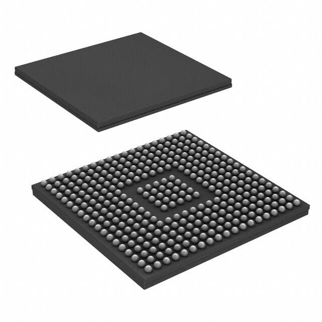


 工商网监
湘ICP备2023018690号
工商网监
湘ICP备2023018690号
