Product
Folder
Sample &
Buy
Support &
Community
Tools &
Software
Technical
Documents
TMP708
SBOS585B – DECEMBER 2011 – REVISED DECEMBER 2016
TMP708 Resistor-Programmable Temperature Switch in SOT Package
1 Features
3 Description
•
The TMP708 is a fully-integrated, resistorprogrammable temperature switch with a temperature
threshold that is set by just one external resistor
within the entire operating range. The TMP708
provides an open-drain, active-low output and has a
2.7-V to 5.5-V supply voltage range.
1
•
•
•
•
•
•
•
Threshold Accuracy:
– ±0.5°C Typical
– ±3°C Maximum (60°C to 100°C)
Temperature Threshold Set By 1% External
Resistor
Low Quiescent Current: 40 μA, Typical
Open-Drain, Active-Low Output Stage
Pin-Selectable 10°C or 30°C Hysteresis
Reset Operation Specified at VCC = 0.8 V
Supply Range: 2.7 V to 5.5 V
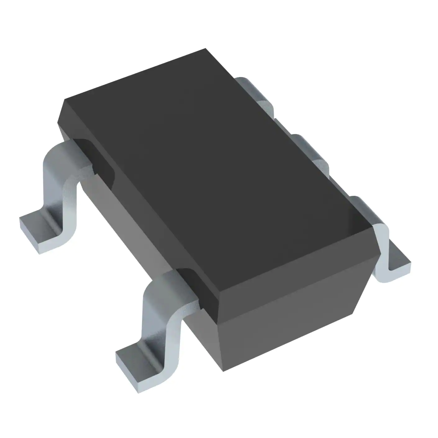
Package: 5-Pin SOT-23
The temperature threshold accuracy is typically
±0.5°C, with a maximum of ±3°C (60°C to 100°C).
The quiescent current consumption is typically 40 μA.
Hysteresis is pin-selectable to 10°C or 30°C.
The TMP708 is available in a 5-pin, SOT-23 package.
Device Information(1)
PART NUMBER
2 Applications
•
•
•
•
•
TMP708
Computers (Laptops and Desktops)
Servers
Industrial and Medical Equipment
Storage Area Networks
Automotive
PACKAGE
SOT-23 (5)
BODY SIZE (NOM)
2.90 mm x 1.60 mm
(1) For all available packages, see the package option addendum
at the end of the datasheet.
Typical Application
150
0.1 …F
2.7 V to 5.5 V
470 k
VCC
VCC
OT
TMP708
Microprocessor
SET
GND
HYST
GND
RSET
Copyright © 2016, Texas Instruments Incorporated
1
An IMPORTANT NOTICE at the end of this data sheet addresses availability, warranty, changes, use in safety-critical applications,
intellectual property matters and other important disclaimers. PRODUCTION DATA.
�TMP708
SBOS585B – DECEMBER 2011 – REVISED DECEMBER 2016
www.ti.com
Table of Contents
1
2
3
4
5
6
7
Features ..................................................................
Applications ...........................................................
Description .............................................................
Revision History.....................................................
Pin Configuration and Functions .........................
Specifications.........................................................
1
1
1
2
3
4
6.1
6.2
6.3
6.4
6.5
6.6
4
4
4
4
5
6
Absolute Maximum Ratings ......................................
ESD Ratings..............................................................
Recommended Operating Conditions.......................
Thermal Information ..................................................
Electrical Characteristics...........................................
Typical Characteristics ..............................................
Detailed Description .............................................. 7
7.1 Overview ................................................................... 7
7.2 Functional Block Diagram ......................................... 7
7.3 Feature Description................................................... 8
7.4 Device Functional Modes.......................................... 8
8
Application and Implementation .......................... 9
8.1 Application Information.............................................. 9
8.2 Typical Application ................................................... 9
9 Power Supply Recommendations...................... 11
10 Layout................................................................... 11
10.1 Layout Guidelines ................................................. 11
10.2 Layout Example .................................................... 11
10.3 Thermal Considerations ........................................ 11
11 Device and Documentation Support ................. 12
11.1
11.2
11.3
11.4
11.5
Receiving Notification of Documentation Updates
Community Resources..........................................
Trademarks ...........................................................
Electrostatic Discharge Caution ............................
Glossary ................................................................
12
12
12
12
12
12 Mechanical, Packaging, and Orderable
Information ........................................................... 12
4 Revision History
NOTE: Page numbers for previous revisions may differ from page numbers in the current version.
Changes from Revision A (February 2012) to Revision B
Page
•
Added Device Information, ESD Ratings, and Recommended Operating Conditions tables, and Detailed
Description, Application and Implementation, Power Supply Recommendations, Layout, Device and Documentation
Support, and Mechanical, Packaging, and Orderable Information sections........................................................................... 1
•
Deleted Package and Ordering Information table; information now available in package option addendum located at
the end of this data sheet ...................................................................................................................................................... 2
Changes from Original (December 2011) to Revision A
Page
•
Updated threshold accuracy feature bullet ............................................................................................................................ 1
•
Updated threshold accuracy text in second paragraph of Description section ...................................................................... 1
•
Updated temperature error parameter in the Electrical Characteristics ................................................................................. 5
2
Submit Documentation Feedback
Copyright © 2011–2016, Texas Instruments Incorporated
Product Folder Links: TMP708
�TMP708
www.ti.com
SBOS585B – DECEMBER 2011 – REVISED DECEMBER 2016
5 Pin Configuration and Functions
DBV Package
5-Pin SOT-23
Top View
SET
1
GND
2
OT
3
5
VCC
4
HYST
Not to scale
Pin Functions
PIN
NAME
NO.
TYPE
DESCRIPTION
GND
2
HYST
4
Analog power Device ground
OT
3
SET
1
Analog input
VCC
5
Analog power Power-supply voltage (2.7 V to 5.5 V)
Digital input
Hysteresis selection. For 10°C, HYST = VCC; for 30°C, HYST = GND.
Digital output Open-drain, active low output
Temperature set point. Connect an external 1% resistor between SET and GND.
Submit Documentation Feedback
Copyright © 2011–2016, Texas Instruments Incorporated
Product Folder Links: TMP708
3
�TMP708
SBOS585B – DECEMBER 2011 – REVISED DECEMBER 2016
www.ti.com
6 Specifications
6.1 Absolute Maximum Ratings
over operating free-air temperature range (unless otherwise noted)
Voltage
Current
(1)
MIN
MAX
Supply, VCC
–0.3
6
Input, SET and HYST
–0.3
VCC + 0.3
Output, OT
–0.3
6
Input
20
Output
20
Operating, TA
Temperature
–40
V
mA
125
Junction, TJ
150
Storatge, Tstg
(1)
UNIT
–65
°C
150
Stresses beyond those listed under Absolute Maximum Ratings may cause permanent damage to the device. These are stress ratings
only, which do not imply functional operation of the device at these or any other conditions beyond those indicated under Recommended
Operating Conditions. Exposure to absolute-maximum-rated conditions for extended periods may affect device reliability.
6.2 ESD Ratings
VALUE
Human-body model (HBM), per ANSI/ESDA/JEDEC JS-001
V(ESD)
(1)
(2)
Electrostatic discharge
(1)
UNIT
±4000
Charged-device model (CDM), per JEDEC specification JESD22-C101 (2)
±1000
Machine model (MM)
±200
V
JEDEC document JEP155 states that 500-V HBM allows safe manufacturing with a standard ESD control process.
JEDEC document JEP157 states that 250-V CDM allows safe manufacturing with a standard ESD control process.
6.3 Recommended Operating Conditions
over operating free-air temperature range (unless otherwise noted)
MIN
VCC
Supply voltage
TA
Operating temperature
NOM
MAX
UNIT
2.7
5.5
V
0
125
°C
6.4 Thermal Information
TMP708
THERMAL METRIC (1)
DBV (SOT-23)
UNIT
5 PINS
RθJA
Junction-to-ambient thermal resistance
217.9
°C/W
RθJC(top)
Junction-to-case (top) thermal resistance
86.3
°C/W
RθJB
Junction-to-board thermal resistance
44.6
°C/W
ψJT
Junction-to-top characterization parameter
4.4
°C/W
ψJB
Junction-to-board characterization parameter
43.8
°C/W
RθJC(bot)
Junction-to-case (bottom) thermal resistance
N/A
°C/W
(1)
4
For more information about traditional and new thermal metrics, see the Semiconductor and IC Package Thermal Metrics application
report.
Submit Documentation Feedback
Copyright © 2011–2016, Texas Instruments Incorporated
Product Folder Links: TMP708
�TMP708
www.ti.com
SBOS585B – DECEMBER 2011 – REVISED DECEMBER 2016
6.5 Electrical Characteristics
at TA = 0°C to 125°C and VCC = 2.7 V to 5.5 V (unless otherwise noted)
PARAMETER
TEST CONDITIONS
MIN
TYP
MAX
UNIT
VCC = 5 V
40
55
µA
VCC = 2.7 V
40
55
µA
±0.5
±3
°C
POWER SUPPLY
ICC
Supply current
TEMPERATURE
TE
Temperature error
TA = 60°C to 100°C
DIGITAL INPUT (HYST)
VIH
High-level input voltage
VIL
Low-level input voltage
Ilkg_in
Input leakage current
CIN
Input capacitance
0.7 × VCC
V
0.3 × VCC
V
1
µA
10
pF
ANALOG INPUT (SET)
VIN
Input voltage range
0
VCC
V
DIGITAL OPEN-DRAIN OUTPUT (OT)
I(OT_SINK)
Output sink current
VOT = 0.3 V
Ilkg(OT)
Output leakage current
VOT = VCC
5
12
mA
1
µA
Submit Documentation Feedback
Copyright © 2011–2016, Texas Instruments Incorporated
Product Folder Links: TMP708
5
�TMP708
SBOS585B – DECEMBER 2011 – REVISED DECEMBER 2016
www.ti.com
6.6 Typical Characteristics
at TA = 25°C and VCC = 2.7 V to 5.5 V (unless otherwise noted)
48
100
VCC = 5 V
VCC = 2.7 V
90
80
44
70
RSET (kW)
Supply Current (mA)
46
42
40
60
50
40
30
38
20
36
10
RSET = 0 W
34
0
0
20
40
60
80
100
120
140
0
20
Temperature (°C)
Figure 1. Supply Current vs Temperature
80
100
120
140
Figure 2. RSET vs Trip Temperature
1.5
10°C Hysteresis
30°C Hysteresis
1
Temperature Error (°C)
30
Hysteresis (°C)
60
Trip Temperature (°C)
35
25
20
15
10
0.5
0
-0.5
-1
5
0
-1.5
0
20
40
60
80
100
120
140
0
Trip Temperature (°C)
20
40
60
80
100
120
140
Trip Temperature (°C)
Figure 3. Hysteresis vs Trip Temperature
6
40
Figure 4. Temperature Error vs Trip Temperature
Submit Documentation Feedback
Copyright © 2011–2016, Texas Instruments Incorporated
Product Folder Links: TMP708
�TMP708
www.ti.com
SBOS585B – DECEMBER 2011 – REVISED DECEMBER 2016
7 Detailed Description
7.1 Overview
The TMP708 is a fully-integrated, resistor-programmable temperature switch that incorporates two temperaturedependent voltage references and one comparator. One voltage reference exhibits a positive temperature
coefficient (tempco), and the other voltage reference exhibits a negative tempco. The temperature at which both
voltage references are equal determines the temperature trip point.
The Functional Block Diagram shows the comparator, the NFET open-drain device connected to the OT pin, the
positive tempco reference using the external RSET resistor, the negative tempco reference, and the hysteresis
control. The voltage of the positive tempco reference is controlled by external resistor RSET.
7.2 Functional Block Diagram
2.7 V to 5.5 V
VCC
HYST
SET
Hysteresis
Control
R PULLUP
Positive
Tempco
Reference
OT
RSET
Negative
Tempco
Reference
TMP708
GND
Copyright © 2016, Texas Instruments Incorporated
Submit Documentation Feedback
Copyright © 2011–2016, Texas Instruments Incorporated
Product Folder Links: TMP708
7
�TMP708
SBOS585B – DECEMBER 2011 – REVISED DECEMBER 2016
www.ti.com
7.3 Feature Description
7.3.1 Temperature Switch
The TMP708 temperature threshold is programmable from 0°C to 125°C and is set by an external 1% resistor
from the SET pin to the GND pin. The TMP708 has an open-drain, active-low output structure that easily
interfaces with a microprocessor.
The TMP708 reaches the temperature trip point when the voltage from the positive tempco reference exceeds
the voltage from the negative tempco reference. This difference causes the output of the comparator to switch
from logic 0 to logic 1. The comparator output drives the gate of the NFET open-drain device, and pulls the
voltage on the OT pin from logic 1 to logic 0 under these conditions; in other words, the output trips.
Furthermore, the logic 1 output from the comparator causes the hysteresis control to increase the voltage of the
positive tempco reference by an amount set by the logic setting on the HYST pin (10°C for logic 1 on the HYST
pin; 30°C for logic 0 on the HYST pin). Increase the voltage of the positive tempco reference after the TMP708
trips to stop the TMP708 from untripping (voltage on the OT pin changing from logic 0 to logic 1) until the local
temperature reduces by the amount set by the HYST pin. After the local temperature reduces, and the voltage
from the positive tempco reference is less than the voltage from the negative tempco reference, the output of the
comparator switches from logic 1 to logic 0. This condition causes the voltage on the OT pin to change from logic
0 to logic 1 (device untrips).
7.3.2 Hysteresis Input
The HYST pin is a digital input that allows the input hysteresis to be set at either 10°C (when HYST = VCC) or
30°C (when HYST = GND). The hysteresis function keeps the OT pin from oscillating when the temperature is
near the threshold. Thus, always connect the HYST pin to either VCC or GND. Other input voltages on this pin
can cause abnormal supply currents or a device malfunction.
7.3.3 Set-Point Resistor (RSET)
Set the temperature threshold by connecting RSET from the SET pin to GND. The value of RSET is determined
using either Figure 2 or Equation 1:
RSET (kΩ) = 0.0012T2 – 0.9308T + 96.147
where
•
T = temperature threshold in degrees Celsius.
(1)
7.4 Device Functional Modes
The TMP708 device has a single functional mode. Normal operation for the TMP708 device occurs when the
power-supply voltage applied across the VCC and GND pins is within the specified operating range of 2.7 V to
5.5 V.
8
Submit Documentation Feedback
Copyright © 2011–2016, Texas Instruments Incorporated
Product Folder Links: TMP708
�TMP708
www.ti.com
SBOS585B – DECEMBER 2011 – REVISED DECEMBER 2016
8 Application and Implementation
NOTE
Information in the following applications sections is not part of the TI component
specification, and TI does not warrant its accuracy or completeness. TI’s customers are
responsible for determining suitability of components for their purposes. Customers should
validate and test their design implementation to confirm system functionality.
8.1 Application Information
The TMP708 device is simple to configure. The only external components that the device requires are a bypass
capacitor and pullup resistor. Power-supply bypassing is strongly recommended. Use a 0.1-µF capacitor placed
as close as possible to the VCC supply pin. To minimize the internal power dissipation of the TMP708 family of
devices, use a pullup resistor value greater than 10 kΩ from the OT pin to the VCC pin. See the Hysteresis Input
section for hysteresis configuration, and the Set-Point Resistor (RSET) section for configuring the temperature
threshold.
8.2 Typical Application
2.7 V to 5.5 V
150
0.1 …F
470 k
VCC
HYST
VCC
OT
TMP708
Microprocessor
SET
GND
GND
RSET
Copyright © 2016, Texas Instruments Incorporated
Figure 5. Overtemperature Protection for a 60°C Trip Point
8.2.1 Design Requirements
For this design example, a 2.7-V to 5.5-V power supply, 60°C trip point, and 10°C hysteresis are used.
Submit Documentation Feedback
Copyright © 2011–2016, Texas Instruments Incorporated
Product Folder Links: TMP708
9
�TMP708
SBOS585B – DECEMBER 2011 – REVISED DECEMBER 2016
www.ti.com
Typical Application (continued)
8.2.2 Detailed Design Procedure
Connect the HYST pin to VCC for 10°C hysteresis. For a 60°C temperature threshold, see the Set-Point Resistor
(RSET) section to compute an ideal RSET resistor value of 44.619 kΩ. Select the closest standard value resistor
available; in this case, 44.2 kΩ. Use a 10-kΩ pullup resistor from the OT pin to the VCC pin. To minimize power,
a larger-value pullup resistor can be used, but must not exceed 470 kΩ. Place a 0.1-μF bypass capacitor close to
the TMP708 device in order to reduce noise coupled from the power supply.
8.2.3 Application Curves
Figure 6 shows an example of the hysteresis feature. The HYST pin is connected to VCC, so the TMP708 device
is configured for 10°C of hysteresis. The device is configured for a 60°C trip temperature by the RSET resistor
value; therefore, the OT output asserts low when the 60°C threshold is exceeded. The OT output remains
asserted low until the sensor reaches 50°C.
OUT
VS
50°C
60°C
T(TRIP)
Figure 6. TMP708 Hysteresis Function
10
Submit Documentation Feedback
Copyright © 2011–2016, Texas Instruments Incorporated
Product Folder Links: TMP708
�TMP708
www.ti.com
SBOS585B – DECEMBER 2011 – REVISED DECEMBER 2016
9 Power Supply Recommendations
The TMP708 low supply current and supply range allow this device to be powered from many sources. Any
significant noise on the VCC pin can result in a trip-point error. Minimize this noise by low-pass filtering the
device supply (VCC) using a 150-Ω resistor and a 0.1-μF capacitor.
10 Layout
10.1 Layout Guidelines
The TMP708 is extremely simple to lay out. Figure 7 shows the recommended board layout.
10.2 Layout Example
VIA to ground plane
VIA to power plane
RSET
150
SET
VCC
0.1 …F
GND
OT
HYST
Figure 7. Recommended Layout
10.3 Thermal Considerations
The TMP708 quiescent current is typically 40 μA. The device dissipates negligible power when the output drives
a high-impedance load. Thus, the die temperature is the same as the package temperature. In order to maintain
accurate temperature monitoring, provide a good thermal contact between the TMP708 package and the device
being monitored. The rise in die temperature as a result of self-heating is given by Equation 2:
ΔTJ = PDISS × θJA
where
•
•
PDISS = power dissipated by the device.
θJA = package thermal resistance. Typical thermal resistance for SOT-23 package is 217.9°C/W.
(2)
To limit the effects of self-heating, keep the output current at a minimum level.
Submit Documentation Feedback
Copyright © 2011–2016, Texas Instruments Incorporated
Product Folder Links: TMP708
11
�TMP708
SBOS585B – DECEMBER 2011 – REVISED DECEMBER 2016
www.ti.com
11 Device and Documentation Support
11.1 Receiving Notification of Documentation Updates
To receive notification of documentation updates, navigate to the device product folder on ti.com. In the upper
right corner, click on Alert me to register and receive a weekly digest of any product information that has
changed. For change details, review the revision history included in any revised document.
11.2 Community Resources
The following links connect to TI community resources. Linked contents are provided "AS IS" by the respective
contributors. They do not constitute TI specifications and do not necessarily reflect TI's views; see TI's Terms of
Use.
TI E2E™ Online Community TI's Engineer-to-Engineer (E2E) Community. Created to foster collaboration
among engineers. At e2e.ti.com, you can ask questions, share knowledge, explore ideas and help
solve problems with fellow engineers.
Design Support TI's Design Support Quickly find helpful E2E forums along with design support tools and
contact information for technical support.
11.3 Trademarks
E2E is a trademark of Texas Instruments.
All other trademarks are the property of their respective owners.
11.4 Electrostatic Discharge Caution
This integrated circuit can be damaged by ESD. Texas Instruments recommends that all integrated circuits be handled with
appropriate precautions. Failure to observe proper handling and installation procedures can cause damage.
ESD damage can range from subtle performance degradation to complete device failure. Precision integrated circuits may be more
susceptible to damage because very small parametric changes could cause the device not to meet its published specifications.
11.5 Glossary
SLYZ022 — TI Glossary.
This glossary lists and explains terms, acronyms, and definitions.
12 Mechanical, Packaging, and Orderable Information
The following pages include mechanical, packaging, and orderable information. This information is the most
current data available for the designated devices. This data is subject to change without notice and revision of
this document. For browser-based versions of this data sheet, refer to the left-hand navigation.
12
Submit Documentation Feedback
Copyright © 2011–2016, Texas Instruments Incorporated
Product Folder Links: TMP708
�PACKAGE OPTION ADDENDUM
www.ti.com
10-Dec-2020
PACKAGING INFORMATION
Orderable Device
Status
(1)
Package Type Package Pins Package
Drawing
Qty
Eco Plan
(2)
Lead finish/
Ball material
MSL Peak Temp
Op Temp (°C)
Device Marking
(3)
(4/5)
(6)
TMP708AIDBVR
ACTIVE
SOT-23
DBV
5
3000
RoHS & Green
NIPDAU
Level-2-260C-1 YEAR
-40 to 125
SBI
TMP708AIDBVT
ACTIVE
SOT-23
DBV
5
250
RoHS & Green
NIPDAU
Level-2-260C-1 YEAR
-40 to 125
SBI
(1)
The marketing status values are defined as follows:
ACTIVE: Product device recommended for new designs.
LIFEBUY: TI has announced that the device will be discontinued, and a lifetime-buy period is in effect.
NRND: Not recommended for new designs. Device is in production to support existing customers, but TI does not recommend using this part in a new design.
PREVIEW: Device has been announced but is not in production. Samples may or may not be available.
OBSOLETE: TI has discontinued the production of the device.
(2)
RoHS: TI defines "RoHS" to mean semiconductor products that are compliant with the current EU RoHS requirements for all 10 RoHS substances, including the requirement that RoHS substance
do not exceed 0.1% by weight in homogeneous materials. Where designed to be soldered at high temperatures, "RoHS" products are suitable for use in specified lead-free processes. TI may
reference these types of products as "Pb-Free".
RoHS Exempt: TI defines "RoHS Exempt" to mean products that contain lead but are compliant with EU RoHS pursuant to a specific EU RoHS exemption.
Green: TI defines "Green" to mean the content of Chlorine (Cl) and Bromine (Br) based flame retardants meet JS709B low halogen requirements of


 工商网监
湘ICP备2023018690号
工商网监
湘ICP备2023018690号
