User's Guide
SLVUAT6A – September 2016 – Revised January 2018
TPA3245 Evaluation Module
This user's guide describes the characteristics, operation, and use of the TPA3245 evaluation module
(EVM). A complete printed-circuit board (PCB) description, schematic diagram, and bill of materials are
also included.
Figure 1. TPA3245 Evaluation Module
1
2
3
4
Contents
Quick Start (BTL Mode) ..................................................................................................... 3
Setup By Mode ............................................................................................................... 5
Hardware Configuration ................................................................................................... 10
EVM Design Documents ................................................................................................. 14
List of Figures
1
TPA3245 Evaluation Module ............................................................................................... 1
SLVUAT6A – September 2016 – Revised January 2018
Submit Documentation Feedback
Copyright © 2016–2018, Texas Instruments Incorporated
TPA3245 Evaluation Module
1
�www.ti.com
2
EVM Board (Top Side) ...................................................................................................... 3
3
EVM Board (Bottom Side) .................................................................................................. 3
4
AIB Input: THD+N vs Frequency
5
AIB Input: THD+N vs Power
6
7
8
9
10
11
12
13
14
15
16
17
18
19
20
21
22
23
24
25
26
27
28
29
30
31
32
.......................................................................................... 5
............................................................................................... 5
Molex™ Input: THD+N vs Frequency .................................................................................... 5
Molex Input: THD+N vs Power ............................................................................................ 5
RCA Input: THD+N vs Frequency ........................................................................................ 5
RCA Input: THD+N vs Power ............................................................................................. 5
AIB Input: THD+N vs Frequency .......................................................................................... 8
AIB Input: THD+N vs Power ............................................................................................... 8
Molex Input: THD+N vs Frequency ....................................................................................... 8
Molex Input: THD+N vs Power ............................................................................................ 8
RCA Input: THD+N vs Frequency ........................................................................................ 8
RCA Input: THD+N vs Power ............................................................................................. 8
AIB Input: THD+N vs Frequency .......................................................................................... 9
AIB Input: THD+N vs Power ............................................................................................... 9
Molex Input: THD+N vs Frequency ..................................................................................... 10
Molex Input: THD+N vs Power .......................................................................................... 10
RCA Input: THD+N vs Frequency ....................................................................................... 10
RCA Input THD+N vs Power ............................................................................................. 10
EVM Power Tree ........................................................................................................... 13
BTL LC Frequency Response ........................................................................................... 13
SE LC Frequency Response ............................................................................................. 13
TPA3245 EVM Top Composite Assembly .............................................................................. 14
TPA3245 EVM Bottom Composite Assembly .......................................................................... 15
TPA3245EVM Board Dimensions ........................................................................................ 16
TPA3245 EVM Top Layer ................................................................................................ 17
TPA3245 EVM Bottom Layer ............................................................................................. 18
TPA3245EVM Schematic 1 ............................................................................................... 19
TPA3245EVM Schematic 2 ............................................................................................... 20
TPA3245EVM Schematic 3 ............................................................................................... 21
List of Tables
1
Jumper Configurations (BTL Mode) ....................................................................................... 4
2
Mode Selection Pins
3
4
5
6
7
8
9
10
........................................................................................................ 5
Jumper Configurations (2.1 BTL Mode) .................................................................................. 6
Jumper Configuration (PBTL Mode) ...................................................................................... 7
Jumper Configuration (SE Mode).......................................................................................... 9
Fault and Clip Overtemperature Status ................................................................................. 10
Frequency Adjust Master Mode Selection .............................................................................. 11
Overcurrent Protection Selection......................................................................................... 11
AIB Connector (J28) Pinout ............................................................................................... 12
TPA3245EVM Bill of Materials ........................................................................................... 22
Trademarks
PurePath is a trademark of Texas Instruments.
CoilCraft is a trademark of Coilcraft, Incorporated.
Molex is a trademark of Molex, LLC.
All other trademarks are the property of their respective owners.
2
TPA3245 Evaluation Module
SLVUAT6A – September 2016 – Revised January 2018
Submit Documentation Feedback
Copyright © 2016–2018, Texas Instruments Incorporated
�Quick Start (BTL Mode)
www.ti.com
1
Quick Start (BTL Mode)
This section describes the necessary hardware, connections, configuration, and steps to quick start the
EVM into bridge-tied load (BTL) mode with stereo audio playing out of two speakers.
1.1
Required Hardware
The EVM requires the following hardware:
• TPA3245EVM (AMPS030-001) power supply 18-V to 36-V DC, 15 A
• Two 2-Ω to 8-Ω, 100-W speakers or resistor loads
• Four speaker or banana cables
• RCA input cables
• Analog output audio source
1.2
Connections and Board Configuration
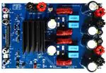
Figure 2 and Figure 3 show both sides of the EVM board.
Figure 2. EVM Board (Top Side)
Figure 3. EVM Board (Bottom Side)
The steps for making the connections are as follows:
1. Set S1 to the RESET position.
2. Set the power supply to 30 V (18-V to 31.5-V range) and current to 10 A (5-A to 14-A range).
3. Connect the power supply to the TPA3245EVM positive terminal to PVDD (J1-RED) and negative
terminal to GND (J1-BLACK).
4. Connect the positive side of the left channel load to the TPA3245EVM OUTA (J9-RED) terminal.
5. Connect the negative side of the left channel load to the TPA3245EVM OUTB (J9-BLACK) terminal.
6. Connect the positive side of the right channel load to the TPA3245EVM OUTC (J2-RED) terminal.
7. Connect the negative side of the right channel load to the TPA3245EVM OUTD (J2-BLACK) terminal.
8. Be careful not to mix up PVDD, OUTA, and OUTC because the colors are the same (RED).
9. Input configuration:
a. Single-ended (SE) inputs: Set J4 and J19 to SE and set J26, J27, J34, and J35 to RCA.
a. Connect the RCA male jack to the female RCA jack input A/AB (J3-RED).
b. Connect the RCA male jack to the female RCA jack input C/CD (J18-WHITE).
b. Differential inputs: Set J4 and J19 to DIFF and set J26, J27, J34, and J35 to RCA.
a. Connect the positive RCA male jack to the female RCA jack input A/AB (J3-RED) and connect
the negative RCA male jack to the female RCA jack input B (J14-BLACK).
SLVUAT6A – September 2016 – Revised January 2018
Submit Documentation Feedback
Copyright © 2016–2018, Texas Instruments Incorporated
TPA3245 Evaluation Module
3
�Quick Start (BTL Mode)
www.ti.com
b. Connect the positive RCA male jack to the female RCA jack input C/CD (J18-RED) and
connect the negative RCA male jack to the female RCA jack input D (J15-BLACK).
c. Analog-Input Board (AIB) input: Set J26, J27, J34, and J35 to AIB.
10. Power up the power supply after correctly making all the connections. The 3.3-V and 12-V LEDs
(GREEN) then illuminate.
11. Set S1 to the NORMAL position.
12. The CLIP_OTW (ORANGE) and FAULT (RED) LEDs must be off if the audio source is off.
Table 1 lists the jumper configurations in BTL mode.
Table 1. Jumper Configurations (BTL Mode)
4
Jumper
Setting
J29
IN
PVDD to 15-V Buck
J31
IN
12-V LDO to 12-V terminal
J32
IN
3.3-V LDO to 3.3-V terminal
J33
IN
3.3-V LDO to 3.3-V terminal
J21
OUT
CSTART SE
J16
3 to 4
Master mode
J5
2 to 3
M1 – BTL
J6
2 to 3
M2 – BTL
J22
IN
OUTA capacitor shunt
J23
IN
OUTB capacitor shunt
J24
IN
OUTC capacitor shunt
J25
IN
OUTD capacitor shunt
J26
2 to 3
INC select
J27
2 to 3
IND select
J7
OUT
PBTL select INC
TPA3245 Evaluation Module
Comment
J8
OUT
PBTL select IND
J10
OUT
INC/D DIFF input
J12
OUT
INC/D DIFF input
J4
1 to 2
INA/B SE input
J19
1 to 2
INC/D SE input
SLVUAT6A – September 2016 – Revised January 2018
Submit Documentation Feedback
Copyright © 2016–2018, Texas Instruments Incorporated
�Setup By Mode
www.ti.com
2
Setup By Mode
The TPA3245EVM is configurable for four different output operations. The 2.0 BTL configuration is the
default set up of the TPA3245EVM as described in Section 1.2. The remaining three configurations are
2.1 BTL plus two SE outputs, 0.1 PBTL output, and 4.0 SE outputs.
Table 2. Mode Selection Pins
Mode Pins
2.1
Input Mode
Output Configuration Description
M2
M1
0
0
2N + 1
2 × BTL
0
1
2N/1N + 1
1 × BTL + 2 × SE
1
0
2N + 1
1 × PBTL
1
1
1N + 1
4 × SE
Stereo BTL output configuration
2.1 BTL + SE mode
Paralleled BTL configuration. Connect INPUT_C and INPUT_D to
GND.
Single-ended output configuration
BTL Mode (Two-Speaker Output)
This mode is the same as described in Section 1.
2.1.1
Performance Data (BTL Mode)
All measurements are taken at an audio frequency = 1 kHz, PVDD_X = 36 V, RL = 4 Ω, fS = 600 kHz,
ROC = 22 kΩ, output filter: L = 7 μH, C = 0.68 µF, with AES17 + AUX-0025 measurement filters.
10
10
1W
20 W
60 W
1
THD+N (%)
THD+N (%)
1
0.1
0.01
0.01
0.001
0.0001
20
0.1
100
1k
Frequency (Hz)
10k
0.001
10
20k
100
D001
Figure 4. AIB Input: THD+N vs Frequency
1k
Power (W)
10k
100k
D009
Figure 5. AIB Input: THD+N vs Power
10
10
1W
20 W
60 W
1
THD+N (%)
THD+N (%)
1
0.1
0.01
0.1
0.01
0.001
0.0001
20
100
1k
Frequency (Hz)
10k
20k
0.001
0.01
D004
Figure 6. Molex™ Input: THD+N vs Frequency
0.1
1
Power (W)
10
100
D012
Figure 7. Molex Input: THD+N vs Power
SLVUAT6A – September 2016 – Revised January 2018
Submit Documentation Feedback
Copyright © 2016–2018, Texas Instruments Incorporated
TPA3245 Evaluation Module
5
�Setup By Mode
www.ti.com
10
10
1W
20 W
60 W
1
THD+N (%)
THD+N (%)
1
0.1
0.01
0.1
0.01
0.001
0.0001
20
200
2000
Frequency (Hz)
0.001
0.01
20000
Figure 8. RCA Input: THD+N vs Frequency
2.2
0.1
D007
1
Power (W)
10
100
D015
Figure 9. RCA Input: THD+N vs Power
BTL MODE (Three-Speaker Output)
OUTC and OUTD are the SE output channels and OUTA and OUTB are the BTL channels for 2.1
operations. OUTC and OUTD can only be in DIFF input mode.
1. Set J6 to L and J5 to H.
2. Remove jumpers J24 and J25.
3. Connect the positive side of the left channel load to OUTC (J2- RED) terminal and the negative side of
the left channel load to the GND (J20) terminal.
4. Connect the positive side of the right channel load to OUTD (J2-BLACK) terminal and the negative
side of the right channel load to the GND (J20) terminal.
5. Connect the positive terminal to OUTA (J9-RED) and the negative terminal to OUTB (J9-BLACK).
6. Set the J19 jumper position to DIFF.
7. Input configuration:
a. SE inputs: Connect the RCA male jack to the female RCA jack input A/AB (J3-RED) and set the J4
jumper positions to SE. Set J26, J27, J34, and J35 to RCA.
b. Differential inputs: Connect the positive RCA male jack to the female RCA jack input A/AB ( J3RED) and connect the negative RCA male jack to the female RCA jack input B (J14-BLACK) and
set the J4 jumper positions to DIFF. Set J26, J27, J34, and J35 to RCA.
c. AIB inputs: Set J26, J27, J34, and J35 to AIB.
Table 3. Jumper Configurations (2.1 BTL Mode)
6
TPA3245 Evaluation Module
Jumper
Setting
J29
IN
Comment
PVDD to 15-V Buck
J32
IN
12-V LDO to 12-V terminal
J33
IN
3.3-V LDO to 3.3-V terminal
J36
IN
12-V LDO to GVDD
J16
3 to 4
Master mode 600 kHz
J22
IN
OUTA capacitor shunt
J23
IN
OUTB capacitor shunt
J24
OUT
OUTC capacitor shunt
J25
OUT
OUTD capacitor shunt
J5
1 to 2
M1 – H
J6
2 to 3
M2 – L
J7
OUT
PBTL SELECT INC
SLVUAT6A – September 2016 – Revised January 2018
Submit Documentation Feedback
Copyright © 2016–2018, Texas Instruments Incorporated
�Setup By Mode
www.ti.com
2.3
PBTL Mode (One-Speaker Output)
This mode uses all four half bridges for a mono output, allowing for the maximum power output from the
device across one load.
2.3.1
1.
2.
3.
4.
5.
Connections and Board Configuration
Set J6 to H and J5 to L.
Connect the positive side of the load to OUTA (J9-RED) and OUTC (J2-RED) terminals (OUTA and
OUTC shorted).
Connect the negative side of the load to OUTB (J9-BLACK) and OUTD (J2-BLACK) terminals (OUTB
and OUTD shorted).
Install PBTL jumpers J7 and J8 (pulls input C and input D to GND).
Input configuration:
a. SE inputs: Connect the RCA male jack to the female RCA jack input A/AB (J3-RED) and set the J4
jumper positions to SE. Set J26, J27, J34, and J35 to RCA.
b. Differential inputs: Connect the positive RCA male jack to the female RCA jack input A/AB (J3RED) and connect the negative RCA male jack to the female RCA jack input B (J14-BLACK). Set
the J4 jumper position to DIFF, and set J26, J27, J34, and J35 to RCA.
c. AIB input: Set J26, J27, J34, and J35 to AIB.
Table 4. Jumper Configuration (PBTL Mode)
Jumper
Setting
J29
IN
Comment
PVDD to 15-V Buck
J31
IN
12-V LDO to 12-V terminal
J32
IN
3.3-V LDO to 3.3-V terminal
J33
IN
3.3-V LDO to 3.3-V terminal
J21
OUT
CSTART SE
J16
3 to 4
Master mode
J5
2 to 3
M1 – PBTL
J6
1 to 2
M2 – PBTL
J22
IN
OUTA capacitor shunt
J23
IN
OUTB capacitor shunt
J24
IN
OUTC capacitor shunt
J25
IN
OUTD capacitor shunt
J26
2 to 3
INC select
J27
2 to 3
IND select
J7
2 to 3
PBTL select INC – GND
J8
2 to 3
PBTL select IND – GND
J10
OUT
INC/D DIFF input
J12
OUT
INC/D DIFF input
J4
1 to 2
INA/B SE input
J19
1 to 2
INC/D SE input
SLVUAT6A – September 2016 – Revised January 2018
Submit Documentation Feedback
Copyright © 2016–2018, Texas Instruments Incorporated
TPA3245 Evaluation Module
7
�Setup By Mode
2.3.2
www.ti.com
Performance Data (PBTL Mode)
All measurements are taken at an audio frequency = 1 kHz, PVDD_X = 36 V, RL = 4 Ω, ƒS = 600 kHz,
ROC = 22 kΩ, output filter: L = 7 μH, C = 0.68 µF, with AES17 + AUX-0025 measurement filters.
10
10
1W
40 W
1
THD+N (%)
THD+N (%)
1
0.1
0.01
0.1
0.01
0.001
0.0001
20
200
2000
Frequency (Hz)
0.001
10
20000
100
D002
Figure 10. AIB Input: THD+N vs Frequency
1k
Power (W)
10k
100k
D010
Figure 11. AIB Input: THD+N vs Power
10
10
1W
40 W
1
THD+N (%)
THD+N (%)
1
0.1
0.01
0.1
0.01
0.001
0.0001
20
100
1k
Frequency (Hz)
0.001
0.01
10k
0.1
D005
Figure 12. Molex Input: THD+N vs Frequency
1
Power (W)
10
100
D013
Figure 13. Molex Input: THD+N vs Power
10
10
1W
40 W
1
THD+N (%)
THD+N (%)
1
0.1
0.01
0.1
0.01
0.001
0.0001
20
100
1k
Frequency (Hz)
10k
20k
Figure 14. RCA Input: THD+N vs Frequency
2.4
0.001
0.01
D008
0.1
1
Power (W)
10
100
D016
Figure 15. RCA Input: THD+N vs Power
SE Mode (Four-Speaker Output)
1. Set J6 to H and J5 to H.
2. Remove jumpers J22, J23, J24, and J25.
3. Connect the positive side of the load to the OUTA (J9-RED) terminal and the negative side of the load
to the GND (J11) terminal.
4. Connect the positive side of the load to the OUTB (J9-BLACK) terminal and the negative side of the
load to the GND (J11) terminal.
5. Connect the positive side of the load to the OUTC (J2-RED) terminal and the negative side of the load
to the GND (J20) terminal.
6. Connect the positive side of the load to the OUTD (J2-BLACK) terminal and the negative side of the
load to the GND (J20) terminal.
7. Set both J4 and J19 jumpers position to DIFF.
8
TPA3245 Evaluation Module
SLVUAT6A – September 2016 – Revised January 2018
Submit Documentation Feedback
Copyright © 2016–2018, Texas Instruments Incorporated
�Setup By Mode
www.ti.com
8. Input configuration:
a. Differential inputs: Set J26, J27, J34, and J35 to RCA.
i. Connect the male RCA jack to the female RCA jack input A/AB (J3-RED) for the OUTA
speaker.
ii. Connect the male RCA jack to the female RCA jack input B (J14-BLACK) for the OUTB
speaker.
iii. Connect the male RCA jack to the female RCA jack input C/CD (J18-WHITE) for the OUTC
speaker.
iv. Connect the male RCA jack to the female RCA jack input D (J15-BLUE) for the OUTD
speaker.
b. AIB input: Set J26, J27, J34, and J35 to AIB.
Table 5. Jumper Configuration (SE Mode)
Jumper
Setting
Comment
J29
IN
PVDD to 15-V Buck
J32
IN
12-V LDO to 12-V terminal
J33
IN
3.3-V LDO to 3.3-V terminal
J36
IN
12-V LDO to GVDD
J16
3 to 4
Master mode 600 kHz
J22
OUT
OUTA capacitor shunt
J23
OUT
OUTB capacitor shunt
J24
OUT
OUTC capacitor shunt
J25
OUT
OUTD capacitor shunt
J5
1 to 2
M1 – H
J6
1 to 2
M2 – H
J7
OUT
PBTL SELECT INC
J8
OUT
PBTL SELECT IND
J4
2 to 3
INA/B DIFF INPUT
J19
2 to 3
INC/D DIFF INPUT
J26
1 to 2
INC-SEL RCA
J27
1 to 2
IND-SEL RCA
J34
1 to 2
INA-SEL RCA
J35
1 to 2
INB-SEL RCA
J21
IN
C_START
NOTE: The performance of the TPA3245EVM and TPA3245D2DDV is dependent on the power
supply. Design the power supply with margins that can deliver the required power. Some
low-frequency applications can require additional bulk capacitance. Replacing the bulk
capacitors on the TPA3245EVM with 3300 µF or more capacitance can be necessary,
depending on the power supply used.
2.4.1
Performance Data (SE Mode)
All measurements are taken at audio frequency = 1 kHz, PVDD_X = 36 V, RL = 4 Ω, ƒS = 600 kHz, ROC =
22 kΩ, output filter: L = 7 μH, C = 0.68 µF, with AES17 + AUX-0025 measurement filters.
SLVUAT6A – September 2016 – Revised January 2018
Submit Documentation Feedback
Copyright © 2016–2018, Texas Instruments Incorporated
TPA3245 Evaluation Module
9
�Hardware Configuration
www.ti.com
10
10
1W
5W
20 W
1
THD+N (%)
THD+N (%)
1
0.1
0.01
0.01
0.001
20
0.1
100
1k
Frequency (Hz)
10k
0.001
0.01
20k
0.1
D003
Figure 16. AIB Input: THD+N vs Frequency
1
Power (W)
10
100
D011
Figure 17. AIB Input: THD+N vs Power
10
10
1W
5W
20 W
1
THD+N (%)
THD+N (%)
1
0.1
0.01
0.001
20
0.1
0.01
100
1k
Frequency (Hz)
10k
0.001
0.01
20k
0.1
D006
Figure 18. Molex Input: THD+N vs Frequency
1
Power (W)
10
100
D014
Figure 19. Molex Input: THD+N vs Power
10
10
1W
5W
20 W
1
THD+N (%)
THD+N (%)
1
0.1
0.01
0.001
20
0.1
0.01
200
2000
Frequency (Hz)
20000
0.001
0.01
D018
Figure 20. RCA Input: THD+N vs Frequency
3
Hardware Configuration
3.1
Indicator Overview (OTW_CLIP and FAULT)
0.1
1
Power (W)
10
100
D017
Figure 21. RCA Input THD+N vs Power
The TPA3245EVM is equipped with LED indicators that illuminate when the FAULT or CLIP_OTW pin (or
both) goes low. See Table 6 and TPA3245 115-W Stereo, 230-W Mono PurePath™ Ultra-HD AnalogInput Class-D Amplifier for more details on which events trigger the pins to go low.
Table 6. Fault and Clip Overtemperature Status
10
FAULT
CLIP_OTW
0
0
Overtemperature (OTE) or overload (OLP) or undervoltage (UVP). Junction temperature higher
than 125°C (overtemperature warning).
0
0
Overload (OLP) or undervoltage (UVP). Junction temperature higher than 125°C (overtemperature
warning).
0
1
Overload (OLP) or undervoltage (UVP). Junction temperature lower than 125°C.
1
0
Junction temperature higher than 125°C (overtemperature warning)
1
1
Junction temperature lower than 125°C and no OLP or UVP faults (normal operation)
TPA3245 Evaluation Module
Description
SLVUAT6A – September 2016 – Revised January 2018
Submit Documentation Feedback
Copyright © 2016–2018, Texas Instruments Incorporated
�Hardware Configuration
www.ti.com
3.2
PWM Frequency Adjust
The TPA3245EVM offers a hardware-trimmed oscillator frequency through the external control of the
FREQ_ADJ pin. Use the frequency adjust to reduce interference problems while using a radio receiver
tuned within the AM band and change the switching frequency from nominal values to lower values (see
Table 7). Choose these values such that the nominal- and the lower-value switching frequencies together
result in the fewest cases of interference throughout the AM band. Select the oscillator frequency based
on the value of the FREQ_ADJ resistor connected to GND in master mode.
Table 7. Frequency Adjust Master Mode Selection
Master Mode
Resistor to GND
PWM Frequency
Nominal
10 kΩ
600 kHz
AM1
20 kΩ
500 kHz
AM2
30 kΩ
450 kHz
For slave-mode operation, turn off the oscillator by pulling the FREQ_ADJ pin to 3.3 V. This action
configures the OSC_I/O pins as inputs, which are to be slaved from an external differential clock. In a
master and slave system, interchannel delay is automatically set up between the switching phases of the
audio channels, which can be illustrated by no idle channels switching at the same time. This setup does
not influence the audio output; rather, only the switch timing to minimize noise coupling between audio
channels through the power supply. In turn, this process optimizes audio performance and results in better
operating conditions for the power supply. The interchannel delay is setup for a slave device depending on
the polarity of the OSC_I/O connection, such that slave mode 1 is selected by connecting OSC_I/O of the
master device in phase with OSC_I/O of the slave device (+ to + and – to –), while slave mode 2 is
selected by connecting the OSC_I/Os out of phase (+ to – and – to +).
3.3
TPA3245EVM Overcurrent Adjust
The TPA3245EVM offers the ability to change the current limit by changing R13 as well as having two
different protection modes; Cycle-by-Cycle Current Control (CB3C) and Latching Shutdown (Latched OC).
For CB3C operations, the resistance must be a value of 22 kΩ to 30 kΩ. For Latched OC operations, the
resistance must be a value of 47 kΩ to 64 kΩ. By default, the resistor R13 is 22 kΩ. Table 8 shows a few
resistance values and their corresponding OC threshold and OC protection mode.
Table 8. Overcurrent Protection Selection
3.4
OC_ADJ Resistor
Value
Protection Mode
OC Threshold
22 kΩ
CB3C
16.3 A
24 kΩ
CB3C
15.1 A
27 kΩ
CB3C
13.5 A
30 kΩ
CB3C
12.3 A
47 kΩ
Latched OC
16.3 A
51 kΩ
Latched OC
15.1 A
56 kΩ
Latched OC
13.5 A
64 kΩ
Latched OC
12.3 A
TPA3245EVM Single-Ended and Differential Inputs
The TPA3245EVM supports both differential and SE inputs. For SE inputs, set either the J4 or J19 jumper
(or both) to the SE position so that the TPA3245EVM uses the OPA1678 operational amplifier (op amp) to
convert the SE input signal to differential to properly drive the differential inputs of the TPA3245 device.
Use input RCA jack J3 to provide INA and INB inputs. Use RCA jack J18 to provide INC and IND inputs
with SE inputs. For differential input operation, set either the J4 or J19 jumpers (or both) to the DIFF
position. The TPA3245EVM uses the OPA1678 to buffer the differential input signal to the differential
inputs of the TPA3245 device. Use input RCA jack J3 to provide INA, RCA jack J14 to provide INB, RCA
jack J18 to provide INC, and RCA jack J15 to provide IND with differential inputs.
SLVUAT6A – September 2016 – Revised January 2018
Submit Documentation Feedback
Copyright © 2016–2018, Texas Instruments Incorporated
TPA3245 Evaluation Module
11
�Hardware Configuration
www.ti.com
NOTE: The SE input settings on the TPA3245EVM must only be used for channels with output
configuration BTL or PBTL, not SE. For SE output configuration, either jumper J4 or J19 (or
both), must be set for that channel to the DIFF position so that the input signal INx is
mapped directly to OUTx.
3.5
Input Connectors
The TPA3245EVM supports three different input connectors. J3, J14, J15, and J18 are RCA connectors.
J10 and J12 are Molex connectors, and J28 is the AIB connector with J30 being the AIB alignment
connection. Table 9 shows the AIB pinout in detail.
Table 9. AIB Connector (J28) Pinout
12
Pin
No.
Function
Audio EVM Input
or Output
1
Amp Out A
Speaker-level output from audio class-D EVM (SE or one side of BTL)
O
2
Amp Out B
Speaker-level output from audio class-D EVM (SE or one side of BTL)
O
O
-
Description
3
PVDD
PVDD voltage supply from audio class-D EVM (variable voltage depending on
class-D EVM use)
4
GND
Ground reference between audio plug-in module and audio class-D EVM
5
NC
-
-
6
NC
-
-
7
3.3 V
3.3-V supply from EVM; used for powering audio plug-in module
O
8
3.3 V
3.3-V supply from EVM; used for powering audio plug-in module
O
9
12 V
12-V supply from EVM; used for powering audio plug-in module
O
10
EN and Reset
Assert enable and reset control for audio class-D EVM (active low)
I
11
Analog IN_A
12
NC
13
Analog IN_B
Analog audio input B (analog in EVM), bit clock I2S bus (digital in EVM)
I
14
CLIP_OTW
Clipping detection, overtemperature warning, or both from audio class-D EVM
(active low)
O
15
Analog IN_C
Analog audio input C (analog in EVM), frame clock I2S bus (digital in EVM)
I
Fault detection from audio class-D EVM (active low)
O
Analog audio input A (analog in EVM), Master I2S bus (digital in EVM)
-
I
-
16
FAULT
17
Analog IN_D
18
NC
-
-
19
NC
-
-
20
NC
-
-
21
GND
Ground reference between audio plug-in module and audio class-D EVM
-
22
GND
Ground reference between audio plug-in module and audio class-D EVM
-
23
NC
-
-
24
NC
-
-
25
NC
-
-
Analog audio Input D (analog in EVM), data in I2S bus (digital in EVM)
26
NC
27
Amp Out C
Speaker-level output from audio class-D EVM (SE or one side of BTL)
O
28
Amp Out D
Speaker-level output from audio class-D EVM (SE or one side of BTL)
O
TPA3245 Evaluation Module
-
I
-
SLVUAT6A – September 2016 – Revised January 2018
Submit Documentation Feedback
Copyright © 2016–2018, Texas Instruments Incorporated
�Hardware Configuration
www.ti.com
3.6
EVM Power Tree
The EVM power section is self-contained with all the necessary onboard voltages generated from the
main PVDD (J1) power input. The PVDD is reduced to 15 V and then used to generate the remaining
required board voltages of 12 V, 5 V, and 3.3 V. Low-dropout linear regulators (LDOs) generate supplies
going to the TPA3245 device itself to reduce the chance of extra added noise. LEDs are provided on the
5-V and 3.3-V supplies for easy verification that the EVM is powered (see Figure 22).
12 V
15 V
PVDD
J29
LM5010ASD
J31
LM2940IMP-12
J32
TLV117-33IDCY
J36
J33
3.3 V
GVDD
Figure 22. EVM Power Tree
3.7
LC Filter Overview
Included near the output of the TPA3245 device are four output LC filters. These output filters filter the
pulse-width modulation (PWM) output, leaving only the audio content at high power, which is fed to the
speakers. The board uses a CoilCraft™ 7-µH inductor and a 0.68-µF film capacitor to form this LC filter.
Using the equations listed in LC Filter Design Application Report, the low-pass filter cutoff is calculated as
follows in Equation 1:
Fcut
off
1
1
2S L u C
2S 7 PH u .68 PF
Figure 23. BTL LC Frequency Response
3.8
72.9 kHz
(1)
Figure 24. SE LC Frequency Response
Post-Filter Feedback (PFFB)
The TPA3245EVM has the footprints available to implement post-filter feedback to improve the audio
performance of the TPA3245 amplifier. For more details on benefits and implementation, see TPA324x
and TPA325x Post-Filter Feedback.
SLVUAT6A – September 2016 – Revised January 2018
Submit Documentation Feedback
Copyright © 2016–2018, Texas Instruments Incorporated
TPA3245 Evaluation Module
13
�Hardware Configuration
3.9
www.ti.com
Reset Circuit
The TPA3245EVM includes RESET supervision so that the TPA3245 device remains in reset until all the
power rails are up and stable. The RESET supervisor also ensures that the device is put into reset if one
of the power rails experiences a brownout. This circuit combined with the RESET switch (S1) help ensure
that the TPA3245 can be placed in reset easily as needed or automatically if there is a power supply
issue.
3.10 Op Amp vs Direct Drive
The op amps are used to change a single-ended input into a differential input. By default, the gain of the
op amps are set for unity gain; however, this can be modified to increase or decrease the gain through the
op amps. One way to bypass the op amps for a more direct connection is using the AIB.
4
EVM Design Documents
This section contains the TPA3245EVM board layout, schematics, and bill of materials (BOM).
4.1
TPA3245EVM Board Layouts
Figure 25 and Figure 26 illustrate the EVM board layouts.
Figure 25. TPA3245 EVM Top Composite Assembly
14
TPA3245 Evaluation Module
SLVUAT6A – September 2016 – Revised January 2018
Submit Documentation Feedback
Copyright © 2016–2018, Texas Instruments Incorporated
�EVM Design Documents
www.ti.com
Figure 26. TPA3245 EVM Bottom Composite Assembly
SLVUAT6A – September 2016 – Revised January 2018
Submit Documentation Feedback
Copyright © 2016–2018, Texas Instruments Incorporated
TPA3245 Evaluation Module
15
�EVM Design Documents
4.2
www.ti.com
TPA3245EVM Board Layouts
Figure 27 shows the EVM board dimensions.
Figure 27. TPA3245EVM Board Dimensions
16
TPA3245 Evaluation Module
SLVUAT6A – September 2016 – Revised January 2018
Submit Documentation Feedback
Copyright © 2016–2018, Texas Instruments Incorporated
�EVM Design Documents
www.ti.com
4.3
TPA3245 EVM Board Debug Plots
Figure 28 and Figure 29 illustrate the TPA3245EVM Debug plots
Figure 28. TPA3245 EVM Top Layer
SLVUAT6A – September 2016 – Revised January 2018
Submit Documentation Feedback
Copyright © 2016–2018, Texas Instruments Incorporated
TPA3245 Evaluation Module
17
�EVM Design Documents
www.ti.com
Figure 29. TPA3245 EVM Bottom Layer
18
TPA3245 Evaluation Module
SLVUAT6A – September 2016 – Revised January 2018
Submit Documentation Feedback
Copyright © 2016–2018, Texas Instruments Incorporated
�EVM Design Documents
www.ti.com
4.4
TPA3245 EVM Schematics
Figure 30 through Figure 32 illustrate the TPA3245EVM schematics.
1
2
3
J34 INA-SEL
C20
J3
1
INA/AB
2
3
LEFT+
INPUT SE A
SE AB
DIFF A+
R9
C17
R7
INA-RCA
C18
22pF
10.0k
10µF
IN-A_RCA
R8
10.0k
100k
R52
0
R4
0
INA-SEL
R47
18.0k
R11
R41
J10


 工商网监
湘ICP备2023018690号
工商网监
湘ICP备2023018690号
