��������
���
���
�
�� ����
��� ��
SLVS365 −MARCH 2001
D Dual Voltage Output, 3.3 V ±3% and
D
D
D
D
D
D
1.8 V ±2%
3.3-V Output Within 2 V of 1.8-V Output
Under All Conditions
1.5-A Load Current Capability on 3.3-V
Output
300-mA Load Current Capability on
1.8-V Output
Overcurrent Protection for Both
Outputs
Thermally-Enhanced Packaging
Concept for Efficient Heat Management
Thermal Shutdown to Protect Device
During Excessive Power Dissipation
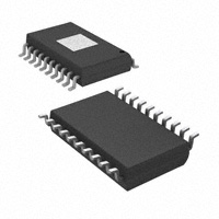
DWP HSOP PACKAGE
(TOP VIEW)
NC
NC
NC
3.3VOUT
NC
5VCC
NC
1.8VOUT
NC
NC
1
2
3
4
5
6
7
8
9
10
20
19
18
17
16
15
14
13
12
11
GND
NC
NC
NC
NC
NC
NC
NC
NC
NC
description
The TPPM0110 is a power source intended for use in systems that have a single 5-V input source and require
dual, linearly-regulated, low-dropout voltage sources. The outputs must track within 2 V of each other during
all conditions and modes of operation. Each output is protected against overcurrent conditions. In the event that
one of the outputs is shorted to ground, the other output must maintain a voltage output differential of less than
2 V compared to the output with the abnormal condition.
The 3.3-V ± 3% regulated output is capable of driving loads of 1.5 A, and the 1.8-V ± 2% regulated output is
capable of driving loads of 300 mA under all normal operating conditions. The device is available in a
PowerPAD thermally-enhanced package for efficient heat management, and requires a copper plane to
dissipate the heat.
Please be aware that an important notice concerning availability, standard warranty, and use in critical applications of
Texas Instruments semiconductor products and disclaimers thereto appears at the end of this data sheet.
PowerPAD is a trademark of Texas Instruments.
Copyright 2001, Texas Instruments Incorporated
�
�����
� ���� ����������� �� ������� �� �� ��!"������� #���$
���#���� ������� �� �������������� ��� �%� ����� �� ��&�� �����������
����#��# '������($ ���#������ ���������) #��� ��� ���������"( ���"�#�
������) �� �"" ����������$
POST OFFICE BOX 655303
• DALLAS, TEXAS 75265
1
���������
���
���
�
�� ����
��� ��
SLVS365 −MARCH 2001
functional block diagram
Bandgap Reference
5VCC
+
3.3VOUT
−
Bandgap
Reference
Startup, Interlock,
Overcurrent, and
Thermal Shutdown
Control
Control
Bandgap Reference
+
−
Control
Startup, Interlock,
Overcurrent, and
Thermal Shutdown
Control
GND
2
POST OFFICE BOX 655303
• DALLAS, TEXAS 75265
1.8VOUT
���������
���
���
�
�� ����
��� ��
SLVS365 −MARCH 2001
Terminal Functions
TERMINAL
NAME
NC
I/O
NO.
DESCRIPTION
1−3,
5, 7,
9−12
13−17†
18,9
I
No connection
3.3VOUT
4
O
3.3-V regulated output
5VCC
6
I
5-V input
1.8VOUT
8
O
1.8-V regulated output
GND
20
I
Ground
† These terminals are to be used for test purposes only, and are not connected in system applications. No signal traces should be connected to
these terminals.
Table 1. Input Selection‡
INPUT CONDITION
3.3VOUT CONDITION
1.8VOUT CONDITION
Power up 0 to 5 V
V(3.3VOUT)
Within 2 V of 1.8VOUT
I(3.3VOUT)
0 to overcurrent limit
V(1.8VOUT)
0 to 1.8 V
I(1.8VOUT)
0 to overcurrent limit
5V
3.3V ±3%
0 to 1.5 A
1.8 V ±2%
0 to 300 mA
Power down 5 V to 0
Within 2 V of 1.8VOUT
1.5 A to 0
1.8 V to 0
300 mA to 0
5V
0V
Up to 5.4 A
1.8 V
0 to 300 mA
5V
Less than 2 V
Don’t care
0V
Up to 1.08 A
Within 2 V of 1.8VOUT
Don’t care
1.8 V to 0
Don’t care
0V
‡ See Figures 2, 3, and 4.
absolute maximum ratings over operating free-air temperature (unless otherwise noted)§
5-V input, V(5VCC) (see Notes 1 and 2) . . . . . . . . . . . . . . . . . . . . . . . . . . . . . . . . . . . . . . . . . . . . . . . . . . . . . . . . 7 V
3.3-V output current limit, IL(3.3VOUT) . . . . . . . . . . . . . . . . . . . . . . . . . . . . . . . . . . . . . . . . . . . . . . . . . . . . . . . 5.4 A
1.8-V output current limit, IL(1.8VOUT) . . . . . . . . . . . . . . . . . . . . . . . . . . . . . . . . . . . . . . . . . . . . . . . . . . . . . . 1.08 A
Continuous power dissipation, PD (see Note 3) . . . . . . . . . . . . . . . . . . . . . . . . . . . . . . . . . . . . . . . . . . . . . . . 3.8 W
Electrostatic discharge susceptibility, V(HBMESD) . . . . . . . . . . . . . . . . . . . . . . . . . . . . . . . . . . . . . . . . . . . . . . 2 kV
Operating ambient temperature range, TA . . . . . . . . . . . . . . . . . . . . . . . . . . . . . . . . . . . . . . . . . . . . . . 0°C to 70°C
Storage temperature range, Tstg . . . . . . . . . . . . . . . . . . . . . . . . . . . . . . . . . . . . . . . . . . . . . . . . . . . −55°C to 150°C
Lead temperature (soldering, 10 sec), T(LEAD) . . . . . . . . . . . . . . . . . . . . . . . . . . . . . . . . . . . . . . . . . . . . . . . 260°C
§ Stresses beyond those listed under “absolute maximum ratings” may cause permanent damage to the device. These are stress ratings only, and
functional operation of the device at these or any other conditions beyond those indicated under “recommended operating conditions” is not
implied. Exposure to absolute-maximum-rated conditions for extended periods may affect device reliability.
NOTES: 1. All voltage values are with respect to GND.
2. Absolute negative voltage values on these terminals should not be below –0.5 V.
3. Assumed correct thermal management technique implementation and ambient temperature of 25°C.
recommended operating conditions
MIN
5-V input, V(5VCC)
Load capacitance, CL
Output load current, IO
4.7
10 mΩ < ESR(CL) < 1 Ω
TYP
MAX
UNIT
5.3
V
100
µF
3.3VOUT
0
1.5
A
1.8VOUT
0
300
mA
0
55
°C
Ambient temperature, TA
POST OFFICE BOX 655303
• DALLAS, TEXAS 75265
3
���������
���
���
�
�� ����
��� ��
SLVS365 −MARCH 2001
electrical characteristics, TA = 0°C to 55°C, CL = 100 µF, V(5VCC) = 5 V (unless otherwise noted)
The operating ratings specified below is interpreted as conditions that do not degrade the device’s parametric
or functional specifications for the life of the product.
PARAMETER
V(5VCC)
TEST CONDITIONS
Input voltage
I(Q)
MIN
TYP
MAX
4.7
5
5.3
IO(3.3VOUT) = 1.2 A and
IO(1.8VOUT) = 300 mA
Quiescent supply current
With no loads on outputs
UNIT
V
1
mA
600
µA
A
Output load current
3.3VOUT = 3.3 V ±3%
1.5
IO
1.8VOUT = 1.8 V ±2%
300
mA
V(3.3VOUT)
V(1.8VOUT)
3.3-V output
IO = 1 mA to 1.2 A
IO = 1 mA to 250 mA
1.8-V output
3.3VOUT
V(DO)
Regulator drop-out
voltage
I(3.3VOUT)OC
Overcurrent protection
I(1.8VOUT)OC
Overcurrent protection
CL
Load capacitance for both
regulated outputs
ESR(CL)
Equivalent series resistance
1.8VOUT
3.33
3.43
V
1.78
1.82
1.85
V
IO < 1.2 A
IO < 250 mA
1
2.5
3.3VOUT, IL↑, See Note 4
2.25
Hysteresis
0.45
Hysteresis
Thermal shutdown hysteresis
0.6
3.4
Hysteresis
TTSD†
5.4
1.08
150
Hysteresis
A
A
mA
100
µF
1
Ω
4.2
V
250
Temperature ↑
V
mA
200
5 V ↓, IO(3.3VOUT)= 1.2 A,
IO(1.8VOUT) = 250 mA
Threshold voltage
3
500
1.8VOUT, See Note 4
Vth
3.23
mV
180
15
°C
† Design targets only. Not tested in production.
NOTE 4: In the event of an overcurrent condition, the output should be a constant current limit such that the current never exceeds 360% of
IO(TYP). Once the overcurrent condition is removed, the device returns to within the specified regulation limits.
electrical characteristics, TA = 0°C to 55°C, CL = 100 µF, V(5VCC) = 5 V (unless otherwise noted)†
The following parametric requirements are applicable to both 3.3VOUT and 1.8VOUT when subjected to these
transient tests.
PARAMETER
TEST CONDITIONS
V(OTL)
Output transient voltage limit
Voltage that load step can affect nominal output
voltage (see Note 5)
IO(STEP)
IO(SLEW)
Output load step current
See Note 5
Output load step current slew rate
See Note 5 and 6
t(STEP)
Output transient time limit
See Note 5
Power up overshoot
Maximum voltage overshoot allowed on either
output when component begins regulation. Voltage
transient time limit is t(STEP) (see Note 5)
MIN
TYP
MAX
−3%
3%
0
IO(TYP)
8
UNIT
A
A/µs
µs
10
7
%
† Design targets only. Not tested in production..
NOTES: 5. Both outputs must maintain voltage regulation within ±3% of nominal, for a load step from 0 to IO(TYP) and from IO(TYP) to 0 A with
a current slew rate of 8A/ms. Load may be toggled at a rate of 20 kHz typical. The outputs must return to the specified regulation
limits within the specified time of 10 µs (typical).
6. Both linear regulators must be capable of regulating small ESR ceramic capacitors or aluminum electrolytic capacitors (see ESR
specification).
4
POST OFFICE BOX 655303
• DALLAS, TEXAS 75265
���������
���
���
�
�� ����
��� ��
SLVS365 −MARCH 2001
thermal characteristics
PARAMETER
RθJC
Thermal impedance, junction-to-case
RθJA
Thermal impedance, junction-to-ambient
MIN
TYP
See Note 7
MAX
UNIT
8
°C/W
33
°C/W
NOTE 7: See JEDEC PCB specifications for high-K and correct implementation for 150 LFM air flow.
TYPICAL CHARACTERISTICS
Bandgap Reference
5VCC
+
3.3VOUT
−
100 µF
0.1 µF
100 µF
0.1 µF
Bandgap
Reference
Startup, Interlock,
Overcurrent, and
Thermal Shutdown
Control
Control
Bandgap Reference
+
−
1.8VOUT
Control
Startup, Interlock,
Overcurrent, and
Thermal Shutdown
Control
GND
NOTE: The 100-µF capacitor has: ESL = 3 nH and ESR = 0.5 Ω to 1 Ω.
Testing circuit includes 100-µF aluminum capacitors which may be replaced with 10-µF ceramic capacitors. Both capacitors must have
equivalent series inductance ESL < 3 nH and equivalent series resistance ESR < 1 Ω.
Figure 1. Test Circuit
POST OFFICE BOX 655303
• DALLAS, TEXAS 75265
5
���������
���
���
�
�� ����
��� ��
SLVS365 −MARCH 2001
TYPICAL CHARACTERISTICS
3.3VOUT
5VCC
1.8VOUT
NOTE: The outputs track within 2 V in the power-up and power-down sequence.
Figure 2. Power-Up and Power-Down Sequence
3.3VOUT
5VCC
1.8VOUT
NOTE: The outputs track within 2 V in the power-up sequence.
Figure 3. Power-Up Sequence
6
POST OFFICE BOX 655303
• DALLAS, TEXAS 75265
���������
���
���
�
�� ����
��� ��
SLVS365 −MARCH 2001
TYPICAL CHARACTERISTICS
3.3VOUT, with
1.5-A Load
5VCC
1.8VOUT
NOTE: The power-up sequence is for an output with 1.5 A on 3.3VOUT.
Figure 4. Power-Up Sequence
5VCC
1.8VOUT
Load Step 1 mA to
300 mA
NOTE: Load regulation on 1.8VOUT with a load step of 1 mA to 300 mA.
Figure 5. Load Regulation on 1.8VOUT
POST OFFICE BOX 655303
• DALLAS, TEXAS 75265
7
���������
���
���
�
�� ����
��� ��
SLVS365 −MARCH 2001
TYPICAL CHARACTERISTICS
5VCC
3.3VOUT
Load Step 1 mA
to 1.5 A
NOTE: Load regulation on 3.3VOUT with a load step of 1 mA to 1.5 A
Figure 6. Load Regulation on 3.3VOUT
5VCC
3.3VOUT
Load Step 1 mA
to 1.5 A
NOTE: Output settling time on 3.3VOUT due to load regulation step of 1 mA to 1.5 A
Figure 7. Settling Time Due to Load Regulation on 3.3VOUT
8
POST OFFICE BOX 655303
• DALLAS, TEXAS 75265
���������
���
���
�
�� ����
��� ��
SLVS365 −MARCH 2001
TYPICAL THERMAL CHARACTERISTICS
To ensure reliable operation of the device, the junction temperature of the output device must be within the safe
operating area (SOA). This is achieved by providing a means to dissipate the heat generated from the junction
of the output structure. There are two components that contribute to thermal resistance. They consist of two
paths in series. The first is the junction-to-case thermal resistance, RθJC; the second is the case-to-ambient
thermal resistance, RθCA. The overall junction-to-ambient thermal resistance, RθJA, is determined by:
RθJA = RθJC + RθCA
The ability to efficiently dissipate the heat from the junction is a function of the package style and board layout
incorporated in the application. The operating junction temperature is determined by the operating ambient
temperature, TA, and the junction power dissipation, PJ.
The junction temperature, TJ, is determined by the following thermal equation:
TJ = TA + PJ (RθJC) + PJ (RθCA)
TJ = TA + PJ (RθJA)
This particular application uses the 20-pin DWP power pad package with a standard lead frame with a dedicated
ground terminal. Using a multilayer printed-circuit board (PCB), the power pad is mounted as recommended
in the TI packaging application. The power pad is electrically connected to the ground plane of the board through
a dedicated ground pin and the die mount power pad. This provides a means for heat spreading through the
copper plane associated within the PCB (ground layer). The thermal resistance from junction to ambient, RθJA,
is dependent of several factors, the implemented method of package attachment to the heat spreading material
and the air flow in the system application.
POST OFFICE BOX 655303
• DALLAS, TEXAS 75265
9
���������
���
���
�
�� ����
��� ��
SLVS365 −MARCH 2001
APPLICATION INFORMATION
packaging
To maximize the efficiency of this package for application on a single layer or multilayer PCB, certain guidelines
must be followed.
The following information is to be used as a guideline only. For further information, refer to the PowerPAD
concept implementation document.
multilayer PCB
The following are guidelines for mounting the PowerPAD IC on a multilayer PCB with a ground plane.
Solid Pad (Land Pattern)
Package Thermal Pad
Thermal Vias
Package Outline
Via = 0,33 mm Diameter
Minimum Pitch Between
Vias is 1,52 mm
Figure 8. Package and Land Configuration for a Multilayer PCB
0,18 mm
(Square)
Package Solder Pad
Component Traces
1,5038 − 1,5748 mm
Component Trace
(2 oz Cu)
2
Plane
4
Plane
1,5748 mm
Thermal Via
Thermal Isolation
Power Plane Only
Package Solder Pad
(Bottom Trace)
Figure 9. Multilayer Board (Side View)
10
POST OFFICE BOX 655303
• DALLAS, TEXAS 75265
1,0142 − 1,0502 mm
Ground Plane
(1 oz Cu)
0,5246 − 0,5606 mm
Power Plane
(1 oz Cu)
0 − 0,071 mm
Board Base and
Bottom Pad
���������
���
���
�
�� ����
��� ��
SLVS365 −MARCH 2001
APPLICATION INFORMATION
In a multilayer board application, the thermal vias are the primary method of heat transfer from the package
thermal pad to the internal ground plane. The efficiency of this method depends on several factors (die area,
number of thermal vias, thickness of copper, etc.). Consult the PowerPAD Thermally Enhanced Package
Technical Brief.
single layer PCB
Use as Much Copper Area
as Possible for Heat Spread
Package Thermal Pad
Package Outline
Figure 10. Land Configuration for Single-Layer PCB
Layout recommendation is to utilize as much copper area for the power management section of a single-layer
board as possible. In a single-layer board application, the thermal pad is attached to a heat spreader (copper
areas) by using a low thermal impedance attachment method (solder paste or thermal-conductive epoxy). In
both of these cases, it is advisable to use as much copper traces as possible to dissipate the heat.
IMPORTANT
If this attachment method is not implemented correctly, this
product will not operate efficiently. Power dissipation capability
will be adversely affected if the device is incorrectly mounted
onto the circuit board.
6
5VCC
100 µF
5VCC
3.3VOUT
4
0.1 µF
0.1 µF
100 µF
0.1 µF
100 µF
†
3.3VOUT
TPPM0110
20-Pin DWP
PowerPAD
Package
20
GND
1.8VOUT
8
†
1.8VOUT
† It is recommended that the capacitors on the outputs (100 µF) have a low ESR < 1 Ω.
These stabilizing capacitors must be placed in close proximity of their corresponding output terminals for optimal performance.
Figure 11. Application Schematic
POST OFFICE BOX 655303
• DALLAS, TEXAS 75265
11
�PACKAGE OPTION ADDENDUM
www.ti.com
10-Dec-2020
PACKAGING INFORMATION
Orderable Device
Status
(1)
Package Type Package Pins Package
Drawing
Qty
Eco Plan
(2)
Lead finish/
Ball material
MSL Peak Temp
Op Temp (°C)
Device Marking
(3)
(4/5)
(6)
TPPM0110DWP
ACTIVE SO PowerPAD
DWP
20
25
RoHS & Green
NIPDAU
Level-2-260C-1 YEAR
0 to 70
TPPM0110
TPPM0110DWPR
ACTIVE SO PowerPAD
DWP
20
2000
RoHS & Green
NIPDAU
Level-2-260C-1 YEAR
0 to 70
TPPM0110
(1)
The marketing status values are defined as follows:
ACTIVE: Product device recommended for new designs.
LIFEBUY: TI has announced that the device will be discontinued, and a lifetime-buy period is in effect.
NRND: Not recommended for new designs. Device is in production to support existing customers, but TI does not recommend using this part in a new design.
PREVIEW: Device has been announced but is not in production. Samples may or may not be available.
OBSOLETE: TI has discontinued the production of the device.
(2)
RoHS: TI defines "RoHS" to mean semiconductor products that are compliant with the current EU RoHS requirements for all 10 RoHS substances, including the requirement that RoHS substance
do not exceed 0.1% by weight in homogeneous materials. Where designed to be soldered at high temperatures, "RoHS" products are suitable for use in specified lead-free processes. TI may
reference these types of products as "Pb-Free".
RoHS Exempt: TI defines "RoHS Exempt" to mean products that contain lead but are compliant with EU RoHS pursuant to a specific EU RoHS exemption.
Green: TI defines "Green" to mean the content of Chlorine (Cl) and Bromine (Br) based flame retardants meet JS709B low halogen requirements of


 工商网监
湘ICP备2023018690号
工商网监
湘ICP备2023018690号
