TPS2074, TPS2075
FOUR-PORT USB HUB POWER CONTROLLERS
SLVS288A – SEPTEMBER 2000 – REVISED FEBRUARY 2001
D
D
D
D
D
D
D
D
D
D
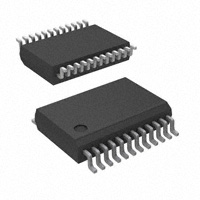
DB PACKAGE
(TOP VIEW)
Complete USB Hub Power Solution
Meets USB Specifications 1.1 and 2.0
Independent Thermal and Short-Circuit
Protection
3.3-V Regulator for USB Hub Controller
Overcurrent Logic Outputs
4.5-V to 5.5-V Operating Range
CMOS- and TTL-Compatible Enable Inputs
185 µA Bus-Power Supply Current
Available in 24-Pin SSOP Package
–40°C to 85°C Ambient Temperature Range
PG_DLY
EN1
AGND
PG
SP
SP
NC
3.3V_OUT
BPMODE†
DP0_RST
EN2
DGND
description
The TPS2074 and TPS2075 provide a complete
USB hub power solution by incorporating three
major functions: current-limited power switches
for four ports, a 3.3-V 100-mA regulator, and a
DP0 line control to signal attach/detach of the hub.
These devices are designed to meet bus-powered and self-powered hub requirements. These
devices are also designed for hybrid hub
implementations and allow for automatic switching from self-powered mode to bus-powered
mode if loss of self-power is experienced. This
feature can be disabled by applying a logic high to
the BP_DIS input
Each port has a current-limited 100-mΩ Nchannel MOSFET high-side power switch for
500 mA self-powered operation. Each port also
has a current-limited 500-mΩ N-channel MOSFET high-side power switch for 100-mA buspowered operation. All the N-channel MOSFETs
are designed without parasitic diodes, preventing
current backflow into the inputs.
For applications where a 5-V regulator is needed,
use the TPS2070 or TPS2071 device.
1
24
2
23
3
22
4
21
5
20
6
19
7
18
8
17
9
16
10
15
11
14
12
13
BP_DIS
BP
OUT1
OUT2
OUT3
OUT4
OC4
OC3
OC2
OC1
EN4
EN3
NC – No internal connection
† Pin 9 is active low (BPMODE) for TPS2074
and active high (BPMODE) for TPS2075.
simplified hybrid-hub diagram‡
D+
D–
Power
Supply
OUT1
SP
5V
GND
OUT2
TPS2074
D+
D–
OUT3
DP0_RST
5V
GND
OUT4
BP
3.3 V_OUT
BPMODE
1.5
kΩ
Downstream
Ports
Upstream
Port
VCC EN OC
Hub
Controller
DM0
5V
GND
5V
GND
DP2
DM2
DP3
DM3
DP4
DM4
DP0
D+
D–
D+
D–
DP1
DM1
D+
D–
5V
GND
‡ See Figure 33 for complete implementation.
SELECTION GUIDE
TA
USB HUB POWER CONTROLLERS
Four port with internal LDO controller
Four-port
PACKAGED DEVICES
PIN COUNT
32
– 40°C to 85°C
Four port without internal LDO controller
Four-port
24
BPMODE
HTSSOP (DAP)
SSOP (DB)†
—
Active low
TPS2070DAP
Active high
TPS2071DAP
—
Active low
—
TPS2074DB
Active high
—
TPS2075DB
† The DB package is available taped and reeled. Add an R suffix to the device type (e.g., TPS2074DBR).
Please be aware that an important notice concerning availability, standard warranty, and use in critical applications of
Texas Instruments semiconductor products and disclaimers thereto appears at the end of this data sheet.
Copyright 2001, Texas Instruments Incorporated
PRODUCTION DATA information is current as of publication date.
Products conform to specifications per the terms of Texas Instruments
standard warranty. Production processing does not necessarily include
testing of all parameters.
POST OFFICE BOX 655303
• DALLAS, TEXAS 75265
1
�TPS2074, TPS2075
FOUR-PORT USB HUB POWER CONTROLLERS
SLVS288A – SEPTEMBER 2000 – REVISED FEBRUARY 2001
functional block diagram
3.3 V/100 mA LDO
3.3 V_OUT
PG
PG_DLY
BP
S1
OUT1
SP
S2
SP
S3
OUT2
S4
S5
OUT3
S6
S7
OUT4
S8
DPO_RST
BP_DIS
AGND
DGND
Control
Logic
EN1
OC1
EN2
OC2
EN3
OC3
EN4
OC4
BPMODE (TPS2074)
BPMODE (TPS2075)
2
POST OFFICE BOX 655303
• DALLAS, TEXAS 75265
�TPS2074, TPS2075
FOUR-PORT USB HUB POWER CONTROLLERS
SLVS288A – SEPTEMBER 2000 – REVISED FEBRUARY 2001
Terminal Functions
TERMINAL
NAME
PG_DLY†
NO.
I/O
1
DESCRIPTION
Adjusts the PG time delay with a capacitor to ground. Adjust the pulse width to fit the application.
EN1
2
I
Active-low enable for OUT1
AGND
3
PG
4
O
Logic output, power good
SP
5
I
Self-power voltage input, connects to local power supply
SP
6
I
Self-power voltage input, connects to local power supply
NC
7
3.3V_OUT
BPMODE‡
8
O
3.3-V internal voltage regulator output
9
O
A logic signal that indicates if the outputs source from the bus-powered supply, BPMODE (TPS2074) or BPMODE
(TPS2075), can be used to signal the hub controller.
DP0_RST
10
O
Connects to DP signal from upstream hub/host through an external 1.5-kΩ resistor
EN2
11
I
Active-low enable for OUT2
DGND
12
EN3
13
EN4
OC1
Analog ground
No internal connection
Digital ground
I
Active-low enable for OUT3
14
I
Active-low enable for OUT4
15
O
Logic output, overcurrent response for OUT1
OC2
16
O
Logic output, overcurrent response for OUT2
OC3
17
O
Logic output, overcurrent response for OUT3
OC4
18
O
Logic output, overcurrent response for OUT4
OUT4
19
O
Power switch output for downstream ports
OUT3
20
O
Power switch output for downstream ports
OUT2
21
O
Power switch output for downstream ports
OUT1
22
O
Power switch output for downstream ports
BP
23
I
Bus power voltage input, connect to VBUS
BP_DIS
24
I
Active-high logic input, disables autoswitch to bus power when self power is disconnected. Connect to BP or GND
† Use the following formula to calculate the capacitance needed;
C = (desired pulse width × 3 × 10⁻⁶ / 1.22
‡ Pin 9 is active low for TPS2074 and active high for TPS2075.
POST OFFICE BOX 655303
• DALLAS, TEXAS 75265
3
�TPS2074, TPS2075
FOUR-PORT USB HUB POWER CONTROLLERS
SLVS288A – SEPTEMBER 2000 – REVISED FEBRUARY 2001
detailed description
BP
The bus-powered supply input (BP) serves as the source for the internal 3.3-V LDO and for all logic functions
in the device. In bus-powered mode, BP also serves as the source for all the outputs (OUTx). If BP is below the
undervoltage threshold, all power switches will turn off and the LDO will be disabled. BP must be connected to
a voltage source in order for the device to operate.
SP
The self-powered supply input (SP) serves as the source for all the outputs (OUTx) in self-powered mode. The
enable logic for the SP switches requires that BP be connected to a voltage source.
OUT1, OUT2, OUT2, OUT4
OUTx are the outputs of the integrated power switches.
3.3V_OUT
The internal 3.3-V LDO output can be used to supply up to 100 mA current to low-power functions, such as hub
controllers.
DP0_RST
DP0_RST functions as a hub reset when a 1.5-kΩ resistor is connected between DP0_RST and the upstream
DP0 data line in a hub system. To provide a clean attach signal on DP0 data line, the DP0_RST output goes
low momentarily (because of the upstream pulldown resistor) to discharge any parasitic charge on the cable,
then goes to 3-state and finally outputs a high signal. The low and Hi-Z pulse widths are adjustable using a
capacitor between PG_DLY and ground, and are approximately 50% of the power-good time delay. Detachment
is signaled by a Hi-Z on DP0_RST. Both DP0_RST and PG will transition high at the same time.
Power Good (PG)
The power good (PG) function serves as a reset for a USB hub controller. PG is asserted low when the output
voltage on the internal voltage regulator is below a fixed threshold. A time delay to ensure a stable output voltage
before PG goes high is adjustable using a small-value ceramic capacitor from PG_DLY to ground.
PG_DLY
PG_DLY connects to an external capacitor to adjust the time delay for PG and DP0_RST. For USB applications,
a 0.1 µF capacitor is recommended, however, reference the USB hub controller data sheet to determine the
needed pulse width criteria.
BP_DIS
BP_DIS is used to enable or disable the autoswitching function between bus-powered mode and self-powered
mode. When BP_DIS is connected low and the voltage on SP is greater than the undervoltage-lockout (UVLO)
threshold, the device will switch to self-powered operation automatically; if the SP voltage falls lower than the
UVLO threshold, the device will switch to bus-powered operation. When BP_DIS is connected high, the
autoswitching function is disabled and the device will not autoswitch to bus-powered operation if the SP voltage
is below the UVLO threshold.
BPMODE or BPMODE
BPMODE (TPS2074) or BPMODE (TPS2075) is an output that signals when the device is in bus-powered
mode. The logic state is set according to the voltages on BP, SP, and BP_DIS. For the TPS2074, BPMODE
outputs a low signal to indicate bus-powered mode or a high signal to indicate self-powered mode. For the
TPS2075, BPMODE outputs a high signal to indicate bus-powered mode or a low signal to indicate self-powered
mode. This output can be used to inform a USB hub controller to configure for bus-powered mode or
self-powered mode.
4
POST OFFICE BOX 655303
• DALLAS, TEXAS 75265
�TPS2074, TPS2075
FOUR-PORT USB HUB POWER CONTROLLERS
SLVS288A – SEPTEMBER 2000 – REVISED FEBRUARY 2001
detailed description (continued)
OC1, OC2, OC3, OC4
OCx is an output signal that is asserted (active low) when an overcurrent or overtemperature condition is
encountered for the corresponding channel. OCx will remain asserted until the overcurrent or overtemperature
condition is removed.
EN1, EN2, EN3, EN4,
The active-low logic input ENx enables or disables the power switches in the device. The enable input is
compatible with both TTL and CMOS logic levels. The switches will not turn on until 3.3V_OUT is above the PG
threshold.
absolute maximum ratings over operating free-air temperature range (unless otherwise noted)†‡
Input voltage range: VI(BP), VI(SP), VI(ENx), VI(BP_DIS) . . . . . . . . . . . . . . . . . . . . . . . . . . . . . . . . . –0.3 V to 6 V
Output voltage range: VO(OUTx) . . . . . . . . . . . . . . . . . . . . . . . . . . . . . . . . . . . . . . . . . . . . . . . . . . . . . –0.3 V to 6 V
VO(3.3V_OUT), VO(PG_DLY), VO(OCx), VO(BPMODE),
VO(DP0_RST), VO(PG) . . . . . . . . . . . . . . . . . . . . . . . . . . . –0.3 V to VO (3.3V_OUT) 0.3 V
Continuous output current: IO(OUTx), IO(3.3V_OUT) . . . . . . . . . . . . . . . . . . . . . . . . . . . . . . . . . . internally limited
Maximum output current:
IO(BPMODE) or IO(BPMODE), IO(DP0_RST), IO(PG), IO(OCx) . . . . . . . . . . ±10 mA
Continuous total power dissipation . . . . . . . . . . . . . . . . . . . . . . . . . . . . . . . . . . . . . . See Dissipation Rating Table
Operating virtual junction temperature range, TJ . . . . . . . . . . . . . . . . . . . . . . . . . . . . . . . . . . . . . . –40°C to 125°C
Storage temperature range, Tstg . . . . . . . . . . . . . . . . . . . . . . . . . . . . . . . . . . . . . . . . . . . . . . . . . . . . –65°C to 150°C
Lead temperature soldering 1,6 mm (1/16 inch) from case for 10 seconds . . . . . . . . . . . . . . . . . . . . . . . 260°C
† Stresses beyond those listed under “absolute maximum ratings” may cause permanent damage to the device. These are stress ratings only, and
functional operation of the device at these or any other conditions beyond those indicated under “recommended operating conditions” is not
implied. Exposure to absolute-maximum-rated conditions for extended periods may affect device reliability.
‡ All voltages are with respect to GND.
DISSIPATION RATING TABLE
PACKAGE
TA ≤ 25°C
POWER RATING
DERATING FACTOR
ABOVE TA = 25°C
TA = 70°C
POWER RATING
TA = 85°C
POWER RATING
24 DB
889.7 mW
8.9 mW/°C
489.3 mW
355.9 mW
recommended operating conditions
Input voltage
Continuous output current, IO
VI(BP)
VI(SP)
VI(BP_DIS)
VI(ENx)
MIN
MAX
4.5
5.5
0
5.5
0
5.5
0
100
SP to OUTx (per switch)
500
BP to 3.3V_OUT
100
-40
POST OFFICE BOX 655303
• DALLAS, TEXAS 75265
V
5.5
BP to OUTx (per switch)
Operating virtual junction temperature, TJ
UNIT
125
mA
°C
5
�TPS2074, TPS2075
FOUR-PORT USB HUB POWER CONTROLLERS
SLVS288A – SEPTEMBER 2000 – REVISED FEBRUARY 2001
electrical characteristics over recommended operating junction temperature range,
4.5 V ≤ VI(BP) ≤ 5.5 V, 4.85 V ≤ VI(SP) ≤ 5.5 V, ENx = 0 V, BP_DIS = 0 V (unless otherwise noted)
input current
TEST CONDITIONS†
PARAMETER
No load
N
l d on OUTx
OUT and
d 3.3V_OUT,
3 3V OUT
ENx = VI(BP)
Input current at BP, switches disabled
II(BP)
N load
l d on OUTx
OUT and
d 3.3V_OUT,
3 3V OUT
No
ENx = 0 V
Input current at BP, switches enabled
No load
N
l d on OUTx
OUT and
d 3.3V_OUT,
3 3V OUT
ENx = VI(SP)
Input current at SP, switches disabled
II(SP)
No load
N
l d on OUTx
OUT and
d 3.3V_OUT,
3 3V OUT
ENx = 0 V
Input current at SP, switches enabled
TYP
MAX
VI(SP) = Hi-Z
VI(SP) = 0 V
MIN
185
240
185
240
VI(SP) = 5 V
VI(SP) = Hi-Z
175
210
185
240
VI(SP) = 0 V
VI(SP) = 5 V
185
240
175
210
VI(BP) = Hi-Z
VI(BP) = 0 V
90
115
90
115
VI(BP) = 5 V
VI(BP) = Hi-Z
115
140
90
115
VI(BP) = 0 V
VI(BP) = 5 V
90
115
115
140
UNIT
µA
µA
µA
µA
† Pulse-testing techniques maintain junction temperature close to ambient temperature; thermal effects must be taken into account separately.
power switches
PARAMETER
Static
drain-source
on-state
resistance
i t
rDS(on)
DS( )
Ilkg(OUTx)
lk (OUT )
TEST CONDITIONS
SP to
OUTx
BP to
OUTx
Leakage current at
OUTx (no load on
3.3V_OUT)
Short circuit current
Short-circuit
(per output)†
MIN
TYP
MAX
VI(SP) = VI(BP) = 5 V
V, IO
0.5
5A
Ox = 0
TA = 25°C
TA = 70°C
100
5V
VI(BP) = 4
4.5
V,
TA = 25°C
TA = 70°C
500
600
900
ENx = VI(BP) = 5.5 V, VI(SP) = Hi-Z,
OUTx connected to ground, VI(VIN) = Hi-Z
TJ = 25°C
0.5
10
ENx = VI(BP) = VI(SP) = 5.5 V,
OUTx connected to ground
TJ = 25°C
0.5
10
ENx = VI(BP) = Hi-Z or 0 V,
VI(SP)= VI(OUTx) = 5.5 V
TJ = 25°C
0.5
10
ENx = VI(BP) = VI(SP) = Hi-Z or 0 V,
VI(OUTx) = 5.5 V
TJ = 25°C
0.5
10
VI(SP) = Open
1A
Open, IOx
0.1
O =0
110
150
UNIT
mΩ
µA
VI(BP) = VI(SP) = 5 V,
OUTx connected to GND,
Device enabled into short circuit
0.6
0.9
1.2
VI(BP) = 5 V, VI(SP) = open,
OUTx connected to GND, device enabled into short
circuit
0.12
0.2
0.3
A
† Pulse-testing techniques maintain junction temperature close to ambient temperature; thermal effects must be taken into account separately.
NOTE: All BP to OUTx , SP to OUTx switches and the internal 3.3-V voltage regulator are loaded to the recommended continuous current rating
of 100 mA, 500 mA and 100 mA, respectively, for the static drain-source on-state resistance measurements.
input signals (ENx, BP_DIS)
PARAMETER
VIH
VIL
High-level input voltage
II
Input current
6
TEST CONDITIONS
MIN
TYP†
MAX
2
Low-level input voltage
0.8
Pullup
ENx (active low)
Pulldown
BP_DIS (active high)
POST OFFICE BOX 655303
VI(ENx) = 0 V
VI(BP_DIS) = 5 V
• DALLAS, TEXAS 75265
5
5
UNIT
V
µA
�TPS2074, TPS2075
FOUR-PORT USB HUB POWER CONTROLLERS
SLVS288A – SEPTEMBER 2000 – REVISED FEBRUARY 2001
electrical characteristics over recommended operating junction temperature range,
4.5 V ≤ VI(BP) ≤ 5.5 V, 4.85 V ≤ VI(SP) ≤ 5.5 V, ENx = 0 V, BP_DIS = 0 V (unless otherwise noted)
(continued)
output signals (BPMODE or BPMODE, OCx, DPO_RST)
PARAMETER
VOH
VOL
TEST CONDITIONS
BPMODE
4.25 V ≤ VI(BP) ≤ 5.5 V,
4.5 V ≤ VI(SP) ≤ 5.5 V
BPMODE
4.25 V ≤ VI(BP) ≤ 5.5 V,
VI(SP) < 4 V
High level output voltage
High-level
Low-level output voltage
OCx
4.25 V ≤ VI(BP) ≤ 5.5 V,
VI(ENx) = 3.3 V or Hi-Z
DPO_RST
4.25 V ≤ VI(BP) ≤ 5.5 V,
VI(PG_DLY) = 3.3 V
BPMODE
4.25 V ≤ VI(BP) ≤ 5.5 V,
VI(SP) < 4 V
BPMODE
4.25 V ≤ VI(BP) ≤ 5.5 V,
4.5 V ≤ VI(SP) ≤ 5.5 V
OCx
4.25 V ≤ VI(BP) ≤ 5.5 V,
OUTx = 0 V
VI(BP)
Minimum input voltage at BP for
low-level output
Ilkg
Hi-Z leakage current at DP0_RST
td
Overcurrent response delay time
(see Note 1)
IO = 300 µA,
IO = 300 µA, VI(SP) = 5 V
MIN
TYP
MAX
UNIT
2.4
2.4
IO = 2 mA
V
2.4
2.4
0.4
IO = 3
3.2
2 mA
0.4
IO(OC) = 3.2 mA
0.4
VO(BPMODE)≤ 0.4 V
VO(BPMODE)≤ 0.4 V,
1.5
0 V ≤ VI(DPO_RST) ≤ 3.3 V, VI(SP) = 0 V,
VI(BP) = 5.5 V, VI(PG_DLY) = 0.9 V
1.5
V
V
–5
5
µA
1
10
ms
NOTE 1: Specified by design, not tested in production.
undervoltage lockout (SP and BP)
PARAMETER
Start threshold
Stop threshold
Vh
hys
Hysteresis voltage (see Note 1)
TEST CONDITIONS
MIN
SP
BP
TYP
MAX
4.5
VI(SP) = Hi-Z
4.25
SP
4
BP
3.75
SP
300
BP
300
UNIT
V
V
mV
NOTE 1: Specified by design, not tested in production.
POST OFFICE BOX 655303
• DALLAS, TEXAS 75265
7
�TPS2074, TPS2075
FOUR-PORT USB HUB POWER CONTROLLERS
SLVS288A – SEPTEMBER 2000 – REVISED FEBRUARY 2001
electrical characteristics over recommended operating junction temperature range,
4.5 V ≤ VI(BP) ≤ 5.5 V, 4.85 V ≤ VI(SP) ≤ 5.5 V, ENx = 0 V, BP_DIS = 0 V, CL(3.3V_OUT) = 10 µF (unless
otherwise noted)
internal voltage regulator
PARAMETER
VO
TEST CONDITIONS
Output voltage, dc
VI(BP) = 4.25 V to 5.5 V,
IO = 100 mA
Dropout voltage
Line regulation
Short-circuit current limit†
Pulldown transistor at 3.3V_OUTPUT
_
(see Note 1)
PSRR
Power-supply ripple rejection (see Note 1)
VI(3.3V_OUT) = 3.3 V
VI(3.3V_OUT) = 1 V
F = 1 kHz, CL(3.3V_OUT)=4.7 µF, ESR=0.25 Ω ,
IO=5 mA, VI(BP)PP=100 mV
Low-level trip threshold voltage at PG
Vhys
VOH
Hysteresis voltage at PG (see Note 1)
VOL
Vref
Low-level output voltage at PG
MAX
3.2
3.3
3.4
V
0.1
%/v
UNIT
V
0.6%
0.12
0.2
0.3
10
40
dB
2.94
50
3
100
2.4
Charge current at PG_DLY
V
mV
V
0.4
Reference voltage at PG_DLY
A
mA
5
2.88
4.25 V ≤ VI(BP) ≤ 5.25 V, IO = 2 mA
4.25 V ≤ VI(BP) ≤ 5.25 V, IO = 3.2 mA
High-level output voltage at PG
TYP
0.6
VI(BP) = 4.25 V to 5.25 V, IO= 5 mA
VI(BP) = 4.25 V,
IO= 5 mA to 100 mA
VI(BP) = 4.25 V, 3.3V_OUT connected to GND
Load regulation
IOS
IO= 5 mA to 100 mA
MIN
V
1.22
V
3
µA
td
Delay time at PG (see Notes 1 and 2)
CL(PG_DLY) = 0.47 µF
190
ms
† Pulse-testing techniques maintain junction temperature close to ambient temperature; thermal effects must be taken into account separately.
NOTES: 1. Specified by design, not tested in production.
2. The PG delay time (td) is calculated using the PG_DLY reference voltage and charge current:
t
+
d
C
V
ref
L(PG_DLY)
Charge Current
power switch timing requirements
TEST CONDITIONS†‡
PARAMETER
ton
toff
ff
tr
tf
Turnon time (see Note 1)
Turnoff time (see Note 1)
Rise time,
time output (see Note 1)
Fall time,
time output (see Note 1)
BP to OUTx
switch
VI(BP) = 5 V, VI(SP) = open,
CL = 100 µF, RL = 50 Ω
SP to OUTx
switch
VI(SP) = VI(BP) = 5 V, TA = 25°C,
CL = 100 µF, RL = 10 Ω
VI(BP) = 5 V, VI(SP) = open, TA = 25°C,
CL = 100 µF, RL = 50 Ω
VI(SP) = VI(BP) = 5 V, TA = 25°C,
CL = 100 µF, RL = 10 Ω
BP to OUTx
switch
SP to OUTx
switch
BP to OUTx
switch
SP to OUTx
switch
BP to OUTx
switch
SP to OUTx
switch
TA = 25°C,
VI(BP) = 5 V, VI(SP) = open, TA = 25°C,
CL = 100 µF, RL = 50 Ω
VI(SP) = VI(BP) = 5 V, TA = 25°C,
CL = 100 µF, RL = 10 Ω
VI(BP) = 5 V, VI(SP) = open, TA = 25°C,
CL = 100 µF, RL = 50 Ω
VI(SP) = VI(BP) = 5 V, TA = 25°C,
CL = 100 µF, RL = 10 Ω
MIN
TYP
MAX
UNIT
4.5
ms
4.5
15
ms
10
4
ms
3
10
ms
3
† Pulse-testing techniques maintain junction temperature close to ambient temperature; thermal effects must be taken into account separately.
‡ All BP to OUTx , SP to OUTx switches and the internal 3.3-V voltage regulator are loaded to the recommended continuous current rating of
100 mA, 500 mA and 100 mA, respectively, for the static drain-source on-state resistance measurements.
NOTE 1. Specified by design, not tested in production.
8
POST OFFICE BOX 655303
• DALLAS, TEXAS 75265
�TPS2074, TPS2075
FOUR-PORT USB HUB POWER CONTROLLERS
SLVS288A – SEPTEMBER 2000 – REVISED FEBRUARY 2001
thermal shutdown
PARAMETER
TJ
Thermal shutdown
Hysteresis
MIN
TYP
First
140
Second
150
First
15
Second
25
50%
VI(ENx)
Current
Meter
MAX
°C
°C
50%
tpd(off)
ton
DUT
toff
tpd(on)
IN
OUT
90%
VO(OUTx)
+
UNIT
10%
90%
10%
tr
tf
90%
VO(OUTx)
10%
90%
10%
TEST CIRCUIT
TIMING
Figure 1. Current Limit Response
Figure 2. Timing and Internal Voltage Regulator
Transition Waveforms
VI(BP) = 5 V
TA = 25°C
CL = 10 µF
RL = 50 Ω
VI(EN)
(2 V/div)
VI(EN)
(2 V/div)
VO(out)
(2 V/div)
VI(BP) = 5 V
TA = 25°C
CL = 10 µF
RL = 50 Ω
VO(OUT)
(2 V/div)
0
2
4
6
8
10 12
t – time – ms
14
16
18
20
Figure 3. Turnon Delay and Rise Time
(BP Switch)
POST OFFICE BOX 655303
0
2
4
6
8
10 12
t – time – ms
14
16
18
20
Figure 4. Turnoff Delay and Fall Time
(BP Switch)
• DALLAS, TEXAS 75265
9
�TPS2074, TPS2075
FOUR-PORT USB HUB POWER CONTROLLERS
SLVS288A – SEPTEMBER 2000 – REVISED FEBRUARY 2001
PARAMETER MEASUREMENT INFORMATION
VI(BP) = VI(SP) = 5 V
TA = 25°C
CL = 10 µF
RL = 10 Ω
VI(BP) = VI(SP) = 5 V
TA = 25°C
CL = 10 µF
RL = 10 Ω
VI(EN)
(2 V/div)
VI(EN)
(2 V/div)
VO(out)
(2 V/div)
VO(OUT)
(2 V/div)
0
2
4
6
8
10 12
t – time – ms
14
16
18
20
0
Figure 5. Turnon Delay and Rise Time
(SP Switch)
2
4
6
VI(BP)
(2 V/div)
VO
3.3V_OUT)
(1 V/div)
VO
(3.3V_OUT)
(1 V/div)
8
12
16 20 24
t – time – ms
28
32
36
40
Figure 7. Turnon Delay and Rise Time
(3.3V_OUT)
10
16
18
20
TA = 25°C
CL = 4.7 µF
RL = 33 Ω
VI(BP)
(2 V/div)
4
14
Figure 6. Turnoff Delay and Fall Time
(SP Switch)
TA = 25°C
CL = 4.7 µF
RL = 33 Ω
0
8
10 12
t – time – ms
POST OFFICE BOX 655303
0
20
40
60
80 100 120 140 160 180 200
t – time – ms
Figure 8. Turnoff Delay and Fall Time
(3.3V_OUT)
• DALLAS, TEXAS 75265
�TPS2074, TPS2075
FOUR-PORT USB HUB POWER CONTROLLERS
SLVS288A – SEPTEMBER 2000 – REVISED FEBRUARY 2001
PARAMETER MEASUREMENT INFORMATION
VO
(3.3V_OUT)
(2 V/div)
VO
(3.3V_OUT)
(2 V/div)
VO
(PG_DLY)
(2 V/div)
VI(BP) = 5 V
TA = 25°C
CL(PG_DLY) = 0.47 µF
0
400
800
1200
VI(BP) = 5 V
TA = 25°C
CL(PG_DLY) = 0.47 µF
VO(PG)
(2 V/div)
1600
2400
3200
4000
2000
2800
3600
t – time – ms
0
Figure 9. PG_DLY Rise Time With a 0.47-µF Capacitor
100 200 300 400 500 600 700 800 900 1000
t – time – ms
Figure 10. Turnon Delay (3.3V_OUT to PG)
VI(BP) = 5 V
TA = 25°C
CL(PG_DLY) = 0.47 µF
VI(BP) = 5 V
TA = 25°C
VO
(3.3V_OUT)
(2 V/div)
VI(EN)
(2 V/div)
VO(PG)
(2 V/div)
IO(OUT)
(0.1A/div)
0
1
2
3
4
5
6
t – time – ms
7
8
9
10
Figure 11. Turnoff Time (3.3V_OUT to PG)
POST OFFICE BOX 655303
0
1
2
3
4
5
6
t – time – ms
7
8
9
10
Figure 12. Short-Circuit Current (BP Switch),
Device Enabled Into Short
• DALLAS, TEXAS 75265
11
�TPS2074, TPS2075
FOUR-PORT USB HUB POWER CONTROLLERS
SLVS288A – SEPTEMBER 2000 – REVISED FEBRUARY 2001
PARAMETER MEASUREMENT INFORMATION
VI(BP) = VI(SP) = 5 V
TA = 25°C
VI(BP) = VI(SP) = 5 V
TA = 25°C
VI(EN)
(2 V/div)
VO(OC)
(2 V/div)
IO(OUT)
(0.5 A/div)
IO(OUT)
(0.5 A/div)
0
1
2
3
4
5
6
t – time – ms
7
8
9
0
10
1
2
3
VO(OC)
(2 V/div)
VO(PG)
(2 V/div)
IO(OUT)
(0.1 A/div)
VO
(3.3V_OUT)
(1 V/div)
2
3
4
5
6
t – time – ms
7
8
9
10
0
2
9
POST OFFICE BOX 655303
4
6
8
10 12
t – time – ms
14
16
18
Figure 16. SP to BP Automatic
Switchover Enabled
Figure 15. OC Response (BP Switch),
Device Enabled Into Short
12
8
10
VI(BP) = 5 V
TA = 25°C
BP_DIS = 0 V or Open
CL(3.3 V_OUT) = 4.7 µF
RL(3.3 V_OUT) = 33 Ω
CL(PG_DLY) = 0.47 µF
VI(BP) = 5 V
TA = 25°C
1
7
Figure 14. OC Response (SP Switch),
Device Enabled Into Short
Figure 13. Short-Circuit Current (SP Switch),
Device Enabled Into Short
0
4
5
6
t – time – ms
• DALLAS, TEXAS 75265
20
�TPS2074, TPS2075
FOUR-PORT USB HUB POWER CONTROLLERS
SLVS288A – SEPTEMBER 2000 – REVISED FEBRUARY 2001
PARAMETER MEASUREMENT INFORMATION
VI(BP) = 5 V
TA = 25°C
BP_DIS = 0 V or Open
VI(BP) = 5 V
TA = 25°C
BP_DIS = 5 V
VO(PG)
(2 V/div)
VO(PG)
(2 V/div)
VO
(3.3V_OUT)
(1 V/div)
VO
(DPO_RST)
(1 V/div)
0
1
2
3
4
5
6
t – time – ms
7
8
9
0
10
Figure 17. SP to BP Automatic
Switchover Disabled
40
80
120 160 200 240 280 320 360 400
t – time – ms
Figure 18. SP to BP Automatic
Switchover Enabled
VI(BP) = 5 V
TA = 25°C
BP_DIS = 5 V
5.25 V
VI(BP)
4.25 V
VO(PG)
(2 V/div)
∆VO
(3.3V_OUT)
(0.05 V/div)
VO
(DPO_RST)
(1 V/div)
TA = 25°C
CL (3.3 V–OUT) = 4.7 µF
IO (3.3 V–OUT) = 100 mA
0
40
80
120 160 200 240 280 320 360 400
t – time – ms
Figure 19. SP to BP Automatic
Switchover Disabled
POST OFFICE BOX 655303
0
100 200 300 400 500 600 700 800 900 1000
t – time – µs
Figure 20. Line Transient Response
• DALLAS, TEXAS 75265
13
�TPS2074, TPS2075
FOUR-PORT USB HUB POWER CONTROLLERS
SLVS288A – SEPTEMBER 2000 – REVISED FEBRUARY 2001
PARAMETER MEASUREMENT INFORMATION
TA = 25°C
CL (3.3 V_OUT) = 10 µF
IO(3.3 V_OUT)
(100 mA/div)
∆VO
(3.3 V_OUT)
(100 mV/div)
0
100 200 300 400 500 600 700 800 900 1000
t – Time – µs
Figure 21. Load Transient Response
TYPICAL CHARACTERISTICS
BP SUPPLY CURRENT
vs
INPUT VOLTAGE
BP SUPPLY CURRENT
vs
JUNCTION TEMPERATURE
205
196
VI(BP) = 5 V
200
192
190
Output Enabled
188
186
184
Output Disabled
182
I I(BP) – Supply Current – µ A
I I(BP) – Supply Current – µ A
194
195
185
Output Disabled
180
175
170
180
–60 –40 –20
0
20
40
60
80
100 120 140
165
4.25
TJ – Junction Temperature – °C
Figure 22
14
Output Enabled
190
4.5
5.25
4.75
5
VI(BP) – Input Voltage – V
Figure 23
POST OFFICE BOX 655303
• DALLAS, TEXAS 75265
5.5
�TPS2074, TPS2075
FOUR-PORT USB HUB POWER CONTROLLERS
SLVS288A – SEPTEMBER 2000 – REVISED FEBRUARY 2001
TYPICAL CHARACTERISTICS
SP SUPPLY CURRENT
vs
INPUT VOLTAGE
SP SUPPLY CURRENT
vs
JUNCTION TEMPERATURE
120
120
VI(SP) = 5 V
115
I I(SP) – Supply Current –
µA
I I(SP) – Supply Current – µ A
115
110
Outputs Disabled
105
Outputs Enabled
100
Outputs Disabled
110
Outputs Enabled
105
100
95
4.5
95
–60 –40 –20 0
20 40 60 80 100 120 140
TJ – Junction Temperature – °C
200
VI(SP) = 5 V
160
140
120
100
80
60
40
20
0
–40
85
0
25
TJ – Junction Temperature – °C
125
DS(on) – Static Drain-Source On-State Resistance – Ω
STATIC DRAIN-SOURCE ON-STATE RESISTANCE
vs
JUNCTION TEMPERATURE
(SELF-POWER SWITCHES)
180
5.5
Figure 25
r
r
DS(on) – Static Drain-Source On-State Resistance – Ω
Figure 24
5
VI(SP) – Input Voltage – V
STATIC DRAIN-SOURCE ON-STATE RESISTANCE
vs
JUNCTION TEMPERATURE
(BUS POWER SWITCHES)
800
700
600
500
400
VI(BP) = 5.5 V
VI(BP) = 4.25 V
300
200
100
0
–40
85
0
25
TJ – Junction Temperature – °C
125
Figure 27
Figure 26
POST OFFICE BOX 655303
• DALLAS, TEXAS 75265
15
�TPS2074, TPS2075
FOUR-PORT USB HUB POWER CONTROLLERS
SLVS288A – SEPTEMBER 2000 – REVISED FEBRUARY 2001
TYPICAL CHARACTERISTICS
SHORT-CIRCUIT OUTPUT CURRENT
vs
JUNCTION TEMPERATURE
(BUS-POWER SWITCHES)
SHORT-CIRCUIT OUTPUT CURRENT
vs
JUNCTION TEMPERATURE
(BUS-POWER SWITCHES)
300
250
VI(BP) = 5.5 V
280
I OS – Short-Circuit Output Current – mA
I OS – Short-Circuit Output Current – mA
VI(BP) = 4.25 V
260
240
220
200
180
160
140
–40
0
25
85
230
210
190
170
150
130
110
–40
125
TJ – Junction Temperature – °C
SHORT-CIRCUIT OUTPUT CURRENT
vs
JUNCTION TEMPERATURE
(SELF-POWER SWITCHES)
I OS – Short-Circuit Output Current – mA
VI(SP) = 5 V
980
960
940
920
900
880
860
840
820
0
25
85
TJ – Junction Temperature – °C
125
VI(BP) – Input Voltage (BP Undervoltage Lockout) – V
INPUT VOLTAGE (BP UNDERVOLTAGE LOCKOUT)
vs
JUNCTION TEMPERATURE
1000
4.25
Start Threshold
4.2
4.15
4.1
4.05
4
3.95
3.9
3.85
Stop Threshold
3.8
3.75
–50
Figure 30
16
125
Figure 29
Figure 28
800
–40
0
25
85
TJ – Junction Temperature – °C
100
0
50
TJ – Junction Temperature – °C
Figure 31
POST OFFICE BOX 655303
• DALLAS, TEXAS 75265
150
�TPS2074, TPS2075
FOUR-PORT USB HUB POWER CONTROLLERS
SLVS288A – SEPTEMBER 2000 – REVISED FEBRUARY 2001
TYPICAL CHARACTERISTICS
VI(SP) – Input Voltage (SP Undervoltage Lockout) – V
INPUT VOLTAGE (SP UNDERVOLTAGE LOCKOUT)
vs
JUNCTION TEMPERATURE
4.5
4.45
Start Threshold
4.4
4.35
4.3
4.25
4.2
4.15
4.1
Stop Threshold
4.05
4
–50
100
0
50
TJ – Junction Temperature – °C
150
Figure 32
APPLICATION INFORMATION
external capacitor requirements
A 0.1-µF ceramic bypass capacitor and a 10-µF bulk capacitor between BP and AGND, close to the device, are
recommended. Similarly, a 0.1-µF ceramic and a 68-µF bulk capacitor, from SP to AGND, and from VEXT to
AGND if an external 5-V LDO is required, are recommended because of much higher current in the self-powered
mode.
From each of the outputs (OUTx) to ground, a 33-µF or higher valued bulk capacitor is recommended when the
output load is heavy. This precaution reduces power-supply transients. Additionally, bypassing the outputs with
a 0.1-µF ceramic capacitor improves the immunity of the device to short-circuit transients.
An output capacitor connected between 3.3V_OUT and GND is required to stabilize the internal control loop.
The internal LDO is designed for a capacitor range of 4.7 µF to 33 µF with an ESR of 0.2 Ω to 10 Ω. Solid
tantalum-electrolytic, aluminum-electrolytic, and multilayer ceramic capacitors are all suitable.
Ceramic capacitors have different types of dielectric material, each exhibiting different temperature and voltage
variations. The most common types are X5R, X7R, Y5U, Z5U, and NPO. The NPO type ceramic capacitors are
generally the most stable over temperature. However, the X5R and X7R are also relatively stable over
temperature (with the X7R being the more stable of the two) and are therefore acceptable for use. The Y5U and
Z5U types provide high capacitance in a small geometry, but exhibit large variations over temperature. For this
reason, the Y5U and Z5U are not generally recommended.
POST OFFICE BOX 655303
• DALLAS, TEXAS 75265
17
�TPS2074, TPS2075
FOUR-PORT USB HUB POWER CONTROLLERS
SLVS288A – SEPTEMBER 2000 – REVISED FEBRUARY 2001
APPLICATION INFORMATION
external capacitor requirements (continued)
A transient condition occurs because of a sudden increase in output current. The output capacitor reduces the
transient effect by providing the additional current needed by the load. Depending on the current demand at the
output, a voltage drop will occur across the internal resistance, ESR, of the capacitor. Using a low ESR capacitor
will help minimize this voltage drop. A larger capacitor will also reduce the voltage drop by supplying the current
demand for a longer time, versus that provided by a smaller capacitor.
overcurrent
An internal sense FET checks for overcurrent conditions. Unlike current-sense resistors, sense FETs do not
increase the series resistance of the current path. When an overcurrent condition is detected, the device
maintains a constant output current and reduces the output voltage accordingly. Complete shutdown occurs
only if the fault is present long enough to activate thermal limiting.
Three possible overload conditions can occur. In the first condition, the output has been shorted before the
device is enabled or before BP and SP have been applied. The TPS2074 and TPS2075 sense the short and
immediately switch into a constant-current output.
In the second condition, the short occurs while the device is enabled. At the instant the short occurs, very high
currents may flow for a very short time before the current-limit circuit can react. After the current-limit circuit has
tripped (reached the overcurrent trip threshold), the device switches into constant-current mode.
In the third condition, the load has been gradually increased beyond the recommended operating current. The
current is permitted to rise until the current-limit threshold is reached or until the thermal limit of the device is
exceeded. The TPS2074 and TPS2075 are capable of delivering current up to the current-limit threshold without
damaging the device. Once the threshold has been reached, the device switches into its constant-current mode.
OC response
The OCx output is asserted (active low) when an overcurrent or overtemperature condition is encountered and
will remain asserted until the overcurrent or overtemperature condition is removed. Connecting a heavy
capacitive load to an enabled device can cause momentary false overcurrent reporting from the inrush current
flowing through the device and charging the downstream capacitor. The TPS2074 and TPS2075 are designed
to reduce false overcurrent reporting by implementing an internal deglitch circuit. This circuit eliminates the need
for an external filter, which requires extra components. Also, using low-ESR electrolytic capacitors on the
outputs can reduce erroneous overcurrent reporting by providing a low-impedance energy source to lower the
inrush current flow through the device during hot-plug events. The OCx outputs are logic outputs thereby
requiring no pullup or pulldown resistors.
18
POST OFFICE BOX 655303
• DALLAS, TEXAS 75265
�TPS2074, TPS2075
FOUR-PORT USB HUB POWER CONTROLLERS
SLVS288A – SEPTEMBER 2000 – REVISED FEBRUARY 2001
APPLICATION INFORMATION
power dissipation and junction temperature
The major source of power dissipation for the TPS2074 and TPS2075 comes from the internal voltage regulator
and the N-channel MOSFETs. Checking the power dissipation and junction temperature is always a good
design practice. Begin by determining the rDS(on) of the N-channel MOSFET according to the input voltage and
operating temperature. As an initial estimate, use the highest operating ambient temperature of interest and
read rDS(on) from the graphs shown under the typical characteristics section of this data sheet. Using this value,
the power dissipation per switch can be calculated by:
PD
+ rDS(on)
I2
Multiply this number by four to get the total power dissipation coming from the N-channel MOSFETs.
ǒ
Ǔ
The power dissipation for the internal voltage regulator is calculated using:
PD
+
V
I(BP)
–V
O(min)
I
O(OUT)
ǒ
The total power dissipation for the device becomes:
P D(total)
+ PD(voltage regulator) )
4
P
D(switch)
Ǔ
Finally, calculate the junction temperature:
TJ
Where:
+ PD
R qJA
) TA
TA = ambient temperature °C
RθJA = Thermal resistance °C /W, equal to inverting of derating factor found on the power dissipation
table in this data sheet.
Compare the calculated junction temperature with the initial estimate. If they do not agree within a few degrees,
repeat the calculation, using the calculated value as the new estimate. Two or three iterations are generally
sufficient to get a reasonable answer.
thermal protection
Thermal protection prevents damage to the IC when heavy-overload or short-circuit faults are present for
extended periods. The faults force the TPS2074 and TPS2075 into constant-current mode at first, which causes
the voltage across the high-side switch to increase; under short-circuit conditions, the voltage across the switch
is equal to the input voltage. The increased dissipation causes the junction temperature to rise to high levels.
The protection circuit senses the junction temperature of the switch and shuts it off. Hysteresis is built into the
thermal sense circuit, and after the device has cooled approximately 20 degrees the switch turns back on. The
switch continues to cycle in this manner until the load fault or input power is removed.
The TPS2074 and TPS2075 implement a dual thermal trip to allow fully independent operation of the power
distribution switches. In an overcurrent or short-circuit condition the junction temperature rises. Once the die
temperature rises to approximately 140°C, the internal thermal-sense circuitry determines which power switch
is in an overcurrent condition and turns only that power switch off, thus isolating the fault without interrupting
operation of the adjacent power switch. If the die temperature exceeds the first thermal trip point of 140°C and
reaches 150°C, the device turns off. The OC output is asserted (active low) when overtemperature or
overcurrent occurs.
POST OFFICE BOX 655303
• DALLAS, TEXAS 75265
19
�TPS2074, TPS2075
FOUR-PORT USB HUB POWER CONTROLLERS
SLVS288A – SEPTEMBER 2000 – REVISED FEBRUARY 2001
APPLICATION INFORMATION
undervoltage lockout (UVLO)
An undervoltage lockout ensures that the device (LDO and switches) is in the off state at power up. The UVLO
will also keep the device from being turned on until the power supply has reached the start threshold (see
undervoltage lockout table), even if the switches are enabled. The UVLO will activate whenever the input
voltage falls below the stop threshold as defined in the undervoltage lockout table. This facilitates the design
of hot-insertion systems where it is not possible to turn off the power switches before input power is removed.
Upon reinsertion, the power switches will be turned on with a controlled rise time to reduce EMI and voltage
overshoots.
self-power to bus-power or bus-power to self-power transition
An autoswitching function between bus-powered mode and self-powered mode is a feature of the TPS2074 and
TPS2075. When this feature is enabled (BP_DIS is inactive) and SP is removed or applied, a transition will be
initiated. The transition sequence begins with the internal LDO being turned off and its external capacitance
discharged. Any enabled switches are also turned off and the external capacitors discharged. Once the LDO
and switch outputs are low, the internal logic will turn the LDO back on. This entire sequence occurs whenever
power to the SP input is removed or applied, regardless of the source of power, i.e., an external power supply
or the use of the external regulator.
universal serial bus (USB) applications
The universal serial bus (USB 1.1) interface is a 12-Mb/s, 1.5-Mb/s, or 480 Mb/s (USB 2.0), multiplexed serial
bus designed for low-to-medium bandwidth PC peripherals (e.g., keyboards, printers, scanners, and mice). The
four-wire USB interface is conceived for dynamic attach-detach (hot plug-unplug) of peripherals. Two lines are
provided for differential data, and two lines are provided for 5-V power distribution.
USB data is a 3.3-V-level signal, but power is distributed at 5 V to allow for voltage drops in cases where power
is distributed through more than one hub or across long cables. Each function must provide its own regulated
3.3 V from the 5-V input or its own internal power supply.
The USB specification defines the following five classes of devices, each differentiated by power-consumption
requirements:
D
D
D
D
D
Hosts/self-powered hubs (SPH)
Bus-powered hubs (BPH)
Low-power, bus-powered functions
High-power, bus-powered functions
Self-powered functions
Self-powered and bus-powered hubs distribute data and power to downstream functions. The TPS2074 and
TPS2075 can provide power-distribution solutions for hybrid hubs that need switching between BPH and SPH
according to power availability and application requirements.
20
POST OFFICE BOX 655303
• DALLAS, TEXAS 75265
�TPS2074, TPS2075
FOUR-PORT USB HUB POWER CONTROLLERS
SLVS288A – SEPTEMBER 2000 – REVISED FEBRUARY 2001
APPLICATION INFORMATION
USB power-distribution requirements
USB can be implemented in several ways, and, regardless of the type of USB device being developed, several
power-distribution features must be implemented.
D
Hosts/self-powered hubs must:
–
–
–
D
Bus-powered hubs must:
–
–
–
–
–
D
Current-limit downstream ports
Report overcurrent conditions on USB VBUS
Output 5.25 V to 4.75 at 500 mA
Enable/disable power to downstream ports
Power up at


 工商网监
湘ICP备2023018690号
工商网监
湘ICP备2023018690号
