Sample &
Buy
Product
Folder
Technical
Documents
Support &
Community
Tools &
Software
TPS22929D
SLVSB39A – DECEMBER 2011 – REVISED JUNE 2014
TPS22929D Ultra-Small, Low on Resistance Load Switch With Controlled Turn-on
1 Features
3 Description
•
•
•
•
The TPS22929D is a small, low rON load switch with
controlled turn on. The device contains a P-channel
MOSFET that can operate over an input voltage
range of 1.4 V to 5.5 V. The switch is controlled by an
on/off input (ON), which is capable of interfacing
directly with low-voltage control signals. The
TPS22929D is active high enable.
1
•
•
•
•
•
•
Integrated Single Load Switch
Small SOT23-6 Package
Input Voltage Range: 1.4 V to 5.5 V
Low ON-Resistance
– rON = 115 mΩ at VIN = 5 V
– rON = 115 mΩ at VIN = 3.3 V
– rON = 118 mΩ at VIN = 2.5 V
– rON = 129 mΩ at VIN = 1.5 V
1.8-A Continuous Switch Current (25°C)
Low Threshold Control Input
Controlled Slew-rate
Under-Voltage Lock Out
Quick Output Discharge
Reverse Current Protection
The TPS22929D contains a 150-Ω on-chip load
resistor for quick output discharge when the switch is
turned off. The rise time of the device is internally
controlled in order to avoid inrush current.
The TPS22929D device provides circuit breaker
functionality by latching off the power-switch during
reverse voltage situations. An internal reverse voltage
comparator disables the power-switch when the
output voltage (VOUT) is driven higher than the input
(VIN) to quickly (10 µs typ) stop the flow of current
towards the input side of the switch. Reverse current
is always active, even when the power-switch is
disabled. Additionally, under-voltage lockout (UVLO)
protection turns the switch off if the input voltage is
too low.
2 Applications
•
•
•
•
•
•
•
•
Portable Industrial Equipment
Portable Medical Equipment
Portable Media Players
Point Of Sales Terminal
GPS Devices
Digital Cameras
Portable Instrumentation
Smartphones
The TPS22929D is available in a small, space-saving
6-pin SOT23 package and is characterized for
operation over the free-air temperature range of
–40°C to 85°C.
Device Information(1)
PART NUMBER
PACKAGE
TPS22929D
BODY SIZE (NOM)
SOT23 (6)
2.90 mm × 1.60 mm
(1) For all available packages, see the orderable addendum at
the end of the datasheet.
4 Simplified Schematic
Power
Supply
VOUT
VIN
ON
CIN
ON
On-State Resistance vs Input Voltage
CL
180
−40C
25C
85C
RL
OFF
160
TPS22929D
GND
140
GND
Ron (mΩ)
120
100
80
60
40
20
0
0
0.5
1
1.5
2
2.5 3 3.5
Voltage (V)
4
4.5
5
5.5
6
G000
1
An IMPORTANT NOTICE at the end of this data sheet addresses availability, warranty, changes, use in safety-critical applications,
intellectual property matters and other important disclaimers. PRODUCTION DATA.
�TPS22929D
SLVSB39A – DECEMBER 2011 – REVISED JUNE 2014
www.ti.com
Table of Contents
1
2
3
4
5
6
7
8
9
Features ..................................................................
Applications ...........................................................
Description .............................................................
Simplified Schematic.............................................
Revision History.....................................................
Pin Configuration and Functions .........................
Specifications.........................................................
1
1
1
1
2
3
3
7.1
7.2
7.3
7.4
7.5
7.6
7.7
3
4
4
4
5
6
7
Absolute Maximum Ratings ......................................
Handling Ratings ......................................................
Recommended Operating Conditions.......................
Thermal Information ..................................................
Electrical Characteristics...........................................
Switching Characteristics ..........................................
Typical Characteristics ..............................................
Parametric Measurement Information ............... 10
Detailed Description ............................................ 12
9.1
9.2
9.3
9.4
Overview .................................................................
Functional Block Diagram .......................................
Feature Description.................................................
Device Functional Modes........................................
12
12
12
13
10 Application and Implementation........................ 14
10.1 Application Information.......................................... 14
10.2 Typical Application ............................................... 14
11 Power Supply Recommendations ..................... 18
12 Layout................................................................... 18
12.1 Layout Guidelines ................................................. 18
12.2 Layout Example .................................................... 19
13 Device and Documentation Support ................. 19
13.1 Trademarks ........................................................... 19
13.2 Electrostatic Discharge Caution ............................ 19
13.3 Glossary ................................................................ 19
14 Mechanical, Packaging, and Orderable
Information ........................................................... 19
5 Revision History
Changes from Original (December 2011) to Revision A
Page
•
Updated to enhanced datasheet standards............................................................................................................................ 1
•
Added Handling Ratings table. .............................................................................................................................................. 4
•
Added Thermal Information table. .......................................................................................................................................... 4
•
Added Detailed Description section. .................................................................................................................................... 12
•
Added Application and Implementation section. ................................................................................................................. 14
•
Added Power Supply Recommendations section. .............................................................................................................. 18
•
Added Layout section. ......................................................................................................................................................... 18
2
Submit Documentation Feedback
Copyright © 2011–2014, Texas Instruments Incorporated
Product Folder Links: TPS22929D
�TPS22929D
www.ti.com
SLVSB39A – DECEMBER 2011 – REVISED JUNE 2014
6 Pin Configuration and Functions
SOT23-6 (DBV) PACKAGE
VOUT
1
6
VIN
GND
2
5
GND
ON
3
4
VIN
Pin Functions
PIN
DESCRIPTION
NAME
DBV
GND
2, 5
ON
3
Switch control input, active high. Do not leave floating
VOUT
1
Switch output
VIN
4, 6
Ground
Switch input, bypass this input with a ceramic capacitor to
ground
7 Specifications
7.1 Absolute Maximum Ratings
over operating free-air temperature range (unless otherwise noted)
MIN
MAX
VIN
Input voltage range
–0.3
6
V
VOUT
Output voltage range
–0.3
6
V
VON
Input voltage range
–0.3
6
V
PMAX
Maximum continuous power dissipation at 25°C
463
Maximum continuous power dissipation at 70°C
254
Maximum continuous power dissipation at 85°C
185
IMAX
Maximum continuous operating current
TA
Operating free-air temperature range
TJ
Maximum junction temperature
–40
UNIT
mW
2
A
85
°C
125
°C
Submit Documentation Feedback
Copyright © 2011–2014, Texas Instruments Incorporated
Product Folder Links: TPS22929D
3
�TPS22929D
SLVSB39A – DECEMBER 2011 – REVISED JUNE 2014
www.ti.com
7.2 Handling Ratings
MIN
Tstg
Storage temperature range
V(ESD)
(1)
(2)
Electrostatic discharge
MAX
UNIT
–65
150
Human body model (HBM), per ANSI/ESDA/JEDEC JS-001, all
pins (1)
–2
2
Charged device model (CDM), per JEDEC specification
JESD22-C101, all pins (2)
–1
1
°C
kV
JEDEC document JEP155 states that 500-V HBM allows safe manufacturing with a standard ESD control process. Pins listed as 2 kV
may actually have higher performance.
JEDEC document JEP157 states that 250-V CDM allows safe manufacturing with a standard ESD control process. Pins listed as 1 kV
may actually have higher performance.
7.3 Recommended Operating Conditions
VIN
Input voltage range
VON
ON voltage range
VOUT
Output voltage range
VIH
High-level input voltage, ON
VIL
Low-level input voltage, ON
CIN
Input Capacitor
(1)
MIN
MAX
1.4
5.5
UNIT
V
0
5.5
V
VIN
VIN = 1.4 V to 5.5 V
1.1
VIN = 3.61 V to 5.5 V
VIN = 1.4 V to 3.6 V
5.5
V
0.6
V
0.4
1
(1)
V
µF
Refer to the application section.
7.4 Thermal Information
TPS22929D
THERMAL METRIC (1)
DBV
UNITS
6 PINS
RθJA
Junction-to-ambient thermal resistance
216
RθJCtop
Junction-to-case (top) thermal resistance
209
RθJB
Junction-to-board thermal resistance
131
ψJT
Junction-to-top characterization parameter
52
ψJB
Junction-to-board characterization parameter
110
(1)
4
°C/W
For more information about traditional and new thermal metrics, see the IC Package Thermal Metrics application report, SPRA953.
Submit Documentation Feedback
Copyright © 2011–2014, Texas Instruments Incorporated
Product Folder Links: TPS22929D
�TPS22929D
www.ti.com
SLVSB39A – DECEMBER 2011 – REVISED JUNE 2014
7.5 Electrical Characteristics
VIN = 1.4 V to 5.5 V, TA = –40ºC to 85ºC (unless otherwise noted)
PARAMETER
IIN
IIN(off)
IIN(Leakage)
Quiescent current
Off supply current
Leakage current
TEST CONDITIONS
TA
MIN
2.2
10
IOUT = 0, VIN = VON = 4.2 V
2.1
7.0
IOUT = 0, VIN = VON = 3.6 V
2.0
7.0
IOUT = 0, VIN = VON = 2.5 V
1.0
5.0
IOUT = 0, VIN = VON = 1.5 V
0.8
5.0
VON = GND, VOUT = Open, VIN = 5.25 V
0.8
10
VON = GND, VOUT = Open, VIN = 4.2 V
0.3
7.0
VON = GND, VOUT = Open, VIN = 3.6 V
Full
0.2
7.0
VON = GND, VOUT = Open, VIN = 2.5 V
0.2
5.0
VON = GND, VOUT = Open, VIN = 1.5 V
0.1
5.0
VON = GND, VOUT = 0, VIN = 5.25 V
0.8
10
VON = GND, VOUT = 0, VIN = 4.2 V
0.3
7.0
0.2
7.0
0.2
5.0
VON = GND, VOUT = 0, VIN = 3.6 V
Full
Full
VON = GND, VOUT = 0, VIN = 1.5 V
VIN = 5.25 V, IOUT = –200 mA
VIN = 5.0 V, IOUT = –200 mA
VIN = 4.2 V, IOUT = –200 mA
On-resistance
VIN = 3.3 V, IOUT = –200 mA
VIN = 2.5 V, IOUT = –200 mA
VIN = 1.5 V, IOUT = –200 mA
RPD
UVLO
25°C
Full
Full
tDELAY
Reverse Current Response
Delay
VIN = 5V
150
150
Product Folder Links: TPS22929D
mΩ
Full
155
180
129
Full
170
200
150
200
1.4
Ω
V
0.50
Full
1
µA
77
mV
10
µs
Submit Documentation Feedback
Copyright © 2011–2014, Texas Instruments Incorporated
µA
175
118
25°C
VIN decreasing, VON 3.6 V, RL = 10 Ω
µA
150
175
115
25°C
Full
VRVP
115
25°C
Under voltage lockout
µA
175
25°C
25°C
VON = 1.4 V to 5.25 V or GND
115
Full
VIN increasing, VON = 3.6 V,
IOUT = –100 mA
Reverse Current Voltage
Threshold
5.0
150
UNIT
175
25°C
VIN = 3.3 V, VON = 0, IOUT = 30 mA
ON input leakage current
0.1
115
Full
Output pull down resistance
ION
MAX
IOUT = 0, VIN = VON = 5.25 V
VON = GND, VOUT = 0, VIN = 2.5 V
rON
TYP
5
�TPS22929D
SLVSB39A – DECEMBER 2011 – REVISED JUNE 2014
www.ti.com
7.6 Switching Characteristics
PARAMETER
TEST CONDITION
TPS22929D
TYP
UNIT
VIN = 5 V, TA = 25ºC (unless otherwise noted)
tON
Turn-ON time
RL = 10 Ω, CL = 0.1 µF
tOFF
Turn-OFF time
RL = 10 Ω, CL = 0.1 µF
7.4
tR
VOUT rise time
RL = 10 Ω, CL = 0.1 µF
3660
tF
VOUT fall time
RL = 10 Ω, CL = 0.1 µF
6.1
3315
µs
VIN = 3.3 V, TA = 25ºC (unless otherwise noted)
tON
Turn-ON time
RL = 10 Ω, CL = 0.1 µF
4655
tOFF
Turn-OFF time
RL = 10 Ω, CL = 0.1 µF
9.5
tR
VOUT rise time
RL = 10 Ω, CL = 0.1 µF
4150
tF
VOUT fall time
RL = 10 Ω, CL = 0.1 µF
3.0
µs
VIN = 1.5 V, TA = 25ºC (unless otherwise noted)
tON
Turn-ON time
RL = 10 Ω, CL = 0.1 µF
tOFF
Turn-OFF time
RL = 10 Ω, CL = 0.1 µF
18.3
tR
VOUT rise time
RL = 10 Ω, CL = 0.1 µF
7812
tF
VOUT fall time
RL = 10 Ω, CL = 0.1 µF
3.0
6
Submit Documentation Feedback
10175
µs
Copyright © 2011–2014, Texas Instruments Incorporated
Product Folder Links: TPS22929D
�TPS22929D
www.ti.com
SLVSB39A – DECEMBER 2011 – REVISED JUNE 2014
7.7 Typical Characteristics
180
6
−40C
25C
85C
160
5
140
4.5
120
4
VOUT (V)
Ron (mΩ)
VIN = 5.0V
VIN = 4.2V
VIN = 3.3V
VIN = 2.5V
VIN = 1.8V
VIN = 1.5V
5.5
100
80
60
3.5
3
2.5
2
1.5
40
1
20
0
0.5
0
0.5
1
1.5
2
2.5 3 3.5
Voltage (V)
4
4.5
5
5.5
0
6
0
0.2
0.4
0.6
0.8
VON (V)
1
1.2
1.4
G000
G000
Figure 1. On-State Resistance vs Input Voltage
Figure 2. On Input Threshold
3000
3.5
−40C
25C
85C
3
−40C
25C
85C
2500
2.5
IIN_Leak (nA)
IIN_Q (µA)
2000
2
1.5
1500
1000
1
500
0.5
0
0
1
2
3
Voltage (V)
4
5
0
6
0
0.5
1
1.5
2
2.5 3 3.5
Voltage (V)
4
4.5
5
5.5
G000
G000
Figure 3. Input Current, Quiescent vs Input Voltage
Figure 4. Input Current, Leak vs Input Voltage
3000
250
225
200
VIN = 1.4V
VIN = 1.5V
VIN = 1.8V
VIN = 2.5V
VIN = 3.3V
VIN = 4.2V
VIN= 5.0V
VIN = 5.5V
−40C
25C
85C
2500
2000
150
IIN_Off (nA)
Ron (mΩ)
175
6
125
100
1500
1000
75
50
500
25
0
−40
−15
10
35
Temperature (°C)
60
85
0
0
G000
Figure 5. On-State Resistance vs Temperature
0.5
1
1.5
2
2.5 3 3.5
Voltage (V)
4
4.5
5
5.5
6
G000
Figure 6. Input Current, Off vs Input Voltage
Submit Documentation Feedback
Copyright © 2011–2014, Texas Instruments Incorporated
Product Folder Links: TPS22929D
7
�TPS22929D
SLVSB39A – DECEMBER 2011 – REVISED JUNE 2014
www.ti.com
Typical Characteristics (continued)
0.8
0.7
Max Power Dissipation (W)
0.6
0.5
0.4
0.3
0.2
0.1
0
−40
−15
10
35
Temperature (°C)
60
85
G000
Figure 7. Allowable Power Dissipation
Figure 8. Under-Voltage Lockout Response
(IOUT = –100mA)
Figure 9. Reverse Current Protection (VIN = 3.0 V, VOUT Ramp up From 3.0 V to 3.3 V)
8
Submit Documentation Feedback
Copyright © 2011–2014, Texas Instruments Incorporated
Product Folder Links: TPS22929D
�TPS22929D
www.ti.com
SLVSB39A – DECEMBER 2011 – REVISED JUNE 2014
7.7.1 Typical AC Characteristics
4500
4
VIN =5.0V, CL = 0.1 µF, RL = 10 Ohms
4000
3500
3
tFall (µs)
tRise (µs)
3000
2500
2000
2
1500
1
1000
500
VIN =5V, CL = 0.1 µF, RL = 10 Ohms
0
−40
−15
10
35
Temperature (°C)
60
0
−40
85
−15
10
35
Temperature (°C)
60
G000
85
G000
Figure 10. Rise Time vs Temperature
Figure 11. Fall Time vs Temperature
10000
10
VIN =1.5V, CL = 0.1 µF, RL = 10 Ohms
9
8000
8
7
6
tFall (µs)
tRise (µs)
6000
4000
5
4
3
2000
2
1
VIN = 1.5V, CL = 0.1 µF, RL = 10 Ohms
0
−40
−15
10
35
Temperature (°C)
60
0
−40
85
−15
10
35
Temperature (°C)
60
G000
85
G000
Figure 12. Rise Time vs Temperature
Figure 13. Fall Time vs Temperature
4500
10
VIN = 5.0V, CL = 0.1 µF, RL = 10 Ohms
4000
8
3500
3000
tOff (µs)
tOn (µs)
6
2500
2000
4
1500
1000
2
500
VIN = 5.0V, CL = 0.1 µF, RL = 10 Ohms
0
−40
−15
10
35
Temperature (°C)
60
85
0
−40
G000
Figure 14. Turn-On Time vs Temperature
−15
10
35
Temperature (°C)
60
85
G000
Figure 15. Turn-Off Time vs Temperature
Submit Documentation Feedback
Copyright © 2011–2014, Texas Instruments Incorporated
Product Folder Links: TPS22929D
9
�TPS22929D
SLVSB39A – DECEMBER 2011 – REVISED JUNE 2014
www.ti.com
Typical AC Characteristics (continued)
15000
25
VIN = 1.5V, CL = 0.1 µF, RL = 10 Ohms
12500
20
10000
tOff (µs)
tOn (µs)
15
7500
10
5000
5
2500
VIN = 1.5V, CL = 0.1 µF, RL = 10 Ohms
0
−40
−15
10
35
Temperature (°C)
60
0
−40
85
−15
10
35
Temperature (°C)
60
85
G000
G000
Figure 16. Turn-On Time vs Temperature
Figure 17. Turn-Off Time vs Temperature
12000
12000
10000
10000
8000
tRise (µs)
tRise (µs)
7500
5000
6000
4000
2500
CL = 1 µF, RL = 10 Ohms, VON = 1.8V
0
0
0.5
1
1.5
2
2.5 3 3.5
VIN (V)
4
2000
−40C
25C
85C
4.5
5
5.5
−40C
25C
85C
CL = 0.1 µF, RL = 10 Ohms, VON = 1.8V
0
6
0
0.5
1
1.5
2
2.5 3 3.5
VIN (V)
4
4.5
5
5.5
G000
6
G000
Figure 18. Rise Time vs Input Voltage
Figure 19. Rise Time vs Input Voltage
8 Parametric Measurement Information
VOUT
VIN
CIN = 1 µF
ON
+
-
(A)
CL
ON
RL
OFF
TPS22929D
GND
GND
A.
GND
Rise and fall times of the control signal is 100 ns.
Figure 20. Test Circuit
10
Submit Documentation Feedback
Copyright © 2011–2014, Texas Instruments Incorporated
Product Folder Links: TPS22929D
�TPS22929D
www.ti.com
SLVSB39A – DECEMBER 2011 – REVISED JUNE 2014
Parametric Measurement Information (continued)
VON
50%
50%
tOFF
tON
VOUT
50%
50%
tf
tr
90%
VOUT
10%
90%
10%
Figure 21. TON/TOFF Waveforms
Submit Documentation Feedback
Copyright © 2011–2014, Texas Instruments Incorporated
Product Folder Links: TPS22929D
11
�TPS22929D
SLVSB39A – DECEMBER 2011 – REVISED JUNE 2014
www.ti.com
9 Detailed Description
9.1 Overview
The TPS22929D is a single channel, 1.8-A load switch in a small, space-saving 6-pin SOT23-6 package. This
devices implement a low resistance P-channel MOSFET with a controlled rise time for applications that need to
limit the inrush current.
This device is also designed to have very low leakage current during off state. This prevents downstream circuits
from pulling high standby current from the supply. Integrated control logic, driver, power supply, and output
discharge FET eliminates the need for additional external components, which reduces solution size and bill of
materials (BOM) count.
9.2 Functional Block Diagram
VIN
Reverse
Current
Protection
UVLO
ON
Control
Logic
VOUT
GND
9.3 Feature Description
9.3.1 On/Off Control
The ON pin controls the state of the switch. Asserting ON high enables the switch. ON is active high and has a
low threshold, making it capable of interfacing with low-voltage signals. The ON pin is compatible with standard
GPIO logic threshold. It can be used with any microcontroller with 1.2-V, 1.8-V, 2.5-V or 3.3-V GPIOs.
9.3.2 Output Pull-Down
The output pull-down is active when the user is turning off the main pass FET. The pull-down discharges the
output rail to approximately 10% of the rail, and then the output pull-down is automatically disconnected to
optimize the shutdown current.
9.3.3 Under-Voltage Lockout
The under-voltage lockout turns-off the switch if the input voltage drops below the under-voltage lockout
threshold. During under-voltage lockout (UVLO), if the voltage level at VOUT exceeds the voltage level at VIN by
the Reverse Current Voltage Threshold (VRVP), the body diode will be disengaged to prevent any current flow to
VIN. With the ON pin active the input voltage rising above the under-voltage lockout threshold will cause a
controlled turn-on of the switch which limits current over-shoots.
12
Submit Documentation Feedback
Copyright © 2011–2014, Texas Instruments Incorporated
Product Folder Links: TPS22929D
�TPS22929D
www.ti.com
SLVSB39A – DECEMBER 2011 – REVISED JUNE 2014
Feature Description (continued)
9.3.4 Reverse Current Protection
In a scenario where VOUT is greater than VIN, there is potential for reverse current through the pass FET or the
body diode. The TPS22929D monitors VIN and VOUT voltage levels. When the reverse current voltage threshold
(VRVP) is exceeded, the switch is disabled (within 10 µs typ). Additionally, the body diode is disengaged so as to
prevent any reverse current flow to VIN. The FET, and the output (VOUT), will resume normal operation when the
reverse voltage scenario is no longer present.
Use the following formula to calculate the amount of reverse current required to activate the protection circuit for
a particular application:
IRC =
0.077V
RON( VIN)
Where,
IRC is the amount of reverse current,
RON(VIN) is the on-resistance as determined by the input voltage.
9.4 Device Functional Modes
Table 1. Function Table
(1)
VOUT to GND (1)
ON
VIN to VOUT
L
OFF
ON
H
ON
OFF
See Output Pull-Down section.
Submit Documentation Feedback
Copyright © 2011–2014, Texas Instruments Incorporated
Product Folder Links: TPS22929D
13
�TPS22929D
SLVSB39A – DECEMBER 2011 – REVISED JUNE 2014
www.ti.com
10 Application and Implementation
10.1 Application Information
10.1.1 VIN to VOUT Voltage Drop
The VIN to VOUT voltage drop in the device is determined by the RON of the device and the load current. The
RON of the device depends upon the VIN condition of the device. Refer to the RON specification of the device in
the Electrical Characteristics table of this datasheet. Once the RON of the device is determined based upon the
VIN conditions, use Equation 1 to calculate the VIN to VOUT voltage drop:
ΔV = ILOAD × RON
(1)
Where,
ΔV = Voltage drop from VIN to VOUT
ILOAD = Load current
RON = On-resistance of the device for a specific VIN
An appropriate ILOAD must be chosen such that the IMAX specification of the device is not violated.
10.1.2 Input Capacitor
To limit the voltage drop on the input supply caused by transient inrush currents, when the switch turns on into a
discharged load capacitor or short-circuit, a capacitor needs to be placed between VIN and GND. A 1-μF ceramic
capacitor, CIN, placed close to the pins is usually sufficient. Higher values of CIN can be used to further reduce
the voltage drop.
10.1.3 Output Capacitor
A CIN to CL ratio of 10 to 1 is recommended for minimizing VIN dip caused by inrush currents during startup.
10.2 Typical Application
Power
Supply
VOUT
VIN
ON
CIN
ON
CL
RL
OFF
TPS22929D
GND
GND
Figure 22. Typical Application Schematic
10.2.1 Design Requirements
Design Parameter
Example Value
VIN
1.5 V to 5 V
CL
0.1 µF to 1 µF
Maximum Acceptable Inrush Current
10 mA
14
Submit Documentation Feedback
Copyright © 2011–2014, Texas Instruments Incorporated
Product Folder Links: TPS22929D
�TPS22929D
www.ti.com
SLVSB39A – DECEMBER 2011 – REVISED JUNE 2014
10.2.2 Detailed Design Procedure
10.2.2.1 Managing Inrush Current
When the switch is enabled, the output capacitors must be charged up from 0-V to VIN voltage. This charge
arrives in the form of inrush current. Inrush current can be calculated using the following equation:
dv
Inrush Current = C ´
dt
(2)
Where,
C = Output capacitance
dv
dt
= Output slew rate
The TPS22929D offers a very slow controlled rise time for minimizing inrush current. This device can be selected
based upon the maximum acceptable slew rate which can be calculated using the design requirements and the
inrush current equation. An output capacitance of 1.0 μF will be used since the amount of inrush increases with
output capacitance:
dv
10 mA = 1.0 μF ´
dt
(3)
dv
= 10 V/ms
dt
(4)
To ensure an inrush current of less than 10 mA, a device with a slew rate less than 10 V/ms must be used.
The TPS22929D has a typical rise time of 4500 μs at 3.3 V . This results in a slew rate of 733 mV/ms which
meets the above design requirements.
Submit Documentation Feedback
Copyright © 2011–2014, Texas Instruments Incorporated
Product Folder Links: TPS22929D
15
�TPS22929D
SLVSB39A – DECEMBER 2011 – REVISED JUNE 2014
www.ti.com
10.2.3 Application Curves
VIN = 5 V
CL = 1 µF
TA = 25°C
RL = 10 Ω
CIN = 10 µF
VIN = 5 V
CL = 1 µF
Figure 23. Turn-On Response
VIN = 5 V
CL = 0.1 µF
TA = 25°C
RL = 10 Ω
TA = 25°C
RL = 10 Ω
CIN = 10 µF
Figure 24. Turn-Off Response
CIN = 1 µF
VIN = 5 V
CL = 0.1 µF
Figure 25. Turn-On Response Time
VIN = 1.5 V
CL = 1 µF
TA = 25°C
RL = 10 Ω
CIN = 10 µF
TA = 25°C
RL = 10 Ω
CIN = 1 µF
Figure 26. Turn-Off Response Time
VIN = 1.5 V
CL = 1 µF
TA = 25°C
RL = 10 Ω
CIN = 10 µF
Figure 28. Turn-Off Response Time
Figure 27. Turn-On Response Time
16
Submit Documentation Feedback
Copyright © 2011–2014, Texas Instruments Incorporated
Product Folder Links: TPS22929D
�TPS22929D
www.ti.com
SLVSB39A – DECEMBER 2011 – REVISED JUNE 2014
VIN = 1.5 V
CL = 0.1 µF
TA = 25°C
RL = 10 Ω
CIN = 1 µF
VIN = 1.5 V
CL = 0.1 µF
Figure 29. Turn-On Response Time
TA = 25°C
RL = 10 Ω
CIN = 1 µF
Figure 30. Turn-Off Response Time
Submit Documentation Feedback
Copyright © 2011–2014, Texas Instruments Incorporated
Product Folder Links: TPS22929D
17
�TPS22929D
SLVSB39A – DECEMBER 2011 – REVISED JUNE 2014
www.ti.com
11 Power Supply Recommendations
The device is designed to operate with a VIN range of 1.4 V to 5.5 V.
12 Layout
12.1 Layout Guidelines
For best performance, all traces should be as short as possible. To be most effective, the input and output
capacitors should be placed close to the device to minimize the effects that parasitic trace inductances may have
on normal operation. Using wide traces for VIN, VOUT, and GND helps minimize the parasitic electrical effects
along with minimizing the case to ambient thermal impedance.
12.1.1 Thermal Considerations
For best device performance, be sure to follow the thermal guidelines in the Thermal Information table. To
calculate max allowable continuous current for your application for a specific VIN and ambient temperature, use
the following formula:
IMAX =
TJ - TA
qJA
RON
Where:
IMAX= Max allowable continuous current
TJ= Max thermal junction temperature (125°C)
TA= Ambient temperature of the application
θJA= Junction-to-air thermal impedance (216°C/W)
RON= RON at a specified input voltage VIN (see Electrical Characteristics)
18
Submit Documentation Feedback
Copyright © 2011–2014, Texas Instruments Incorporated
Product Folder Links: TPS22929D
�TPS22929D
www.ti.com
SLVSB39A – DECEMBER 2011 – REVISED JUNE 2014
12.2 Layout Example
GND
VIN
VIN
GND
VIN
VIN Bypass
Capacitor
VIN
GND
Via
GND
Via
GND
VOUT
ON
GND
ON
To GPIO
control
VOUT
VOUT Bypass
Capacitor
Figure 31. Layout Drawing
13 Device and Documentation Support
13.1 Trademarks
All trademarks are the property of their respective owners.
13.2 Electrostatic Discharge Caution
These devices have limited built-in ESD protection. The leads should be shorted together or the device placed in conductive foam
during storage or handling to prevent electrostatic damage to the MOS gates.
13.3 Glossary
SLYZ022 — TI Glossary.
This glossary lists and explains terms, acronyms, and definitions.
14 Mechanical, Packaging, and Orderable Information
The following pages include mechanical, packaging, and orderable information. This information is the most
current data available for the designated devices. This data is subject to change without notice and revision of
this document. For browser-based versions of this data sheet, refer to the left-hand navigation.
Submit Documentation Feedback
Copyright © 2011–2014, Texas Instruments Incorporated
Product Folder Links: TPS22929D
19
�PACKAGE OPTION ADDENDUM
www.ti.com
30-Jun-2014
PACKAGING INFORMATION
Orderable Device
Status
(1)
Package Type Package Pins Package
Drawing
Qty
Eco Plan
Lead/Ball Finish
MSL Peak Temp
(2)
(6)
(3)
Op Temp (°C)
Device Marking
(4/5)
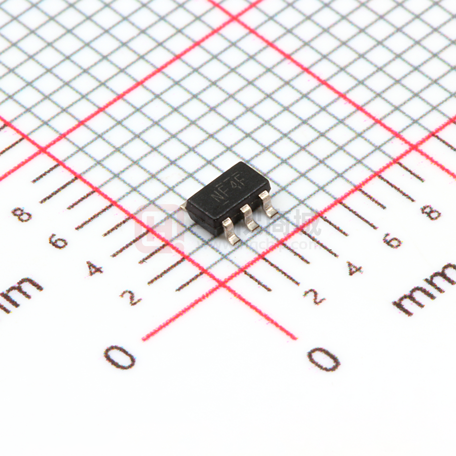
TPS22929DDBVR
ACTIVE
SOT-23
DBV
6
3000
Green (RoHS
& no Sb/Br)
CU NIPDAU
Level-1-260C-UNLIM
-40 to 85
NF4F
TPS22929DDBVT
ACTIVE
SOT-23
DBV
6
250
Green (RoHS
& no Sb/Br)
CU NIPDAU
Level-1-260C-UNLIM
-40 to 85
NF4F
(1)
The marketing status values are defined as follows:
ACTIVE: Product device recommended for new designs.
LIFEBUY: TI has announced that the device will be discontinued, and a lifetime-buy period is in effect.
NRND: Not recommended for new designs. Device is in production to support existing customers, but TI does not recommend using this part in a new design.
PREVIEW: Device has been announced but is not in production. Samples may or may not be available.
OBSOLETE: TI has discontinued the production of the device.
(2)
Eco Plan - The planned eco-friendly classification: Pb-Free (RoHS), Pb-Free (RoHS Exempt), or Green (RoHS & no Sb/Br) - please check http://www.ti.com/productcontent for the latest availability
information and additional product content details.
TBD: The Pb-Free/Green conversion plan has not been defined.
Pb-Free (RoHS): TI's terms "Lead-Free" or "Pb-Free" mean semiconductor products that are compatible with the current RoHS requirements for all 6 substances, including the requirement that
lead not exceed 0.1% by weight in homogeneous materials. Where designed to be soldered at high temperatures, TI Pb-Free products are suitable for use in specified lead-free processes.
Pb-Free (RoHS Exempt): This component has a RoHS exemption for either 1) lead-based flip-chip solder bumps used between the die and package, or 2) lead-based die adhesive used between
the die and leadframe. The component is otherwise considered Pb-Free (RoHS compatible) as defined above.
Green (RoHS & no Sb/Br): TI defines "Green" to mean Pb-Free (RoHS compatible), and free of Bromine (Br) and Antimony (Sb) based flame retardants (Br or Sb do not exceed 0.1% by weight
in homogeneous material)
(3)
MSL, Peak Temp. - The Moisture Sensitivity Level rating according to the JEDEC industry standard classifications, and peak solder temperature.
(4)
There may be additional marking, which relates to the logo, the lot trace code information, or the environmental category on the device.
(5)
Multiple Device Markings will be inside parentheses. Only one Device Marking contained in parentheses and separated by a "~" will appear on a device. If a line is indented then it is a continuation
of the previous line and the two combined represent the entire Device Marking for that device.
(6)
Lead/Ball Finish - Orderable Devices may have multiple material finish options. Finish options are separated by a vertical ruled line. Lead/Ball Finish values may wrap to two lines if the finish
value exceeds the maximum column width.
Important Information and Disclaimer:The information provided on this page represents TI's knowledge and belief as of the date that it is provided. TI bases its knowledge and belief on information
provided by third parties, and makes no representation or warranty as to the accuracy of such information. Efforts are underway to better integrate information from third parties. TI has taken and
continues to take reasonable steps to provide representative and accurate information but may not have conducted destructive testing or chemical analysis on incoming materials and chemicals.
TI and TI suppliers consider certain information to be proprietary, and thus CAS numbers and other limited information may not be available for release.
Addendum-Page 1
Samples
�PACKAGE OPTION ADDENDUM
www.ti.com
30-Jun-2014
In no event shall TI's liability arising out of such information exceed the total purchase price of the TI part(s) at issue in this document sold by TI to Customer on an annual basis.
Addendum-Page 2
�PACKAGE MATERIALS INFORMATION
www.ti.com
1-Jul-2014
TAPE AND REEL INFORMATION
*All dimensions are nominal
Device
Package Package Pins
Type Drawing
SPQ
Reel
Reel
A0
Diameter Width (mm)
(mm) W1 (mm)
TPS22929DDBVR
SOT-23
DBV
6
3000
178.0
9.0
TPS22929DDBVT
SOT-23
DBV
6
250
178.0
9.0
Pack Materials-Page 1
B0
(mm)
K0
(mm)
P1
(mm)
W
Pin1
(mm) Quadrant
3.23
3.17
1.37
4.0
8.0
Q3
3.23
3.17
1.37
4.0
8.0
Q3
�PACKAGE MATERIALS INFORMATION
www.ti.com
1-Jul-2014
*All dimensions are nominal
Device
Package Type
Package Drawing
Pins
SPQ
Length (mm)
Width (mm)
Height (mm)
TPS22929DDBVR
SOT-23
DBV
6
3000
180.0
180.0
18.0
TPS22929DDBVT
SOT-23
DBV
6
250
180.0
180.0
18.0
Pack Materials-Page 2
�PACKAGE OUTLINE
DBV0006A
SOT-23 - 1.45 mm max height
SCALE 4.000
SMALL OUTLINE TRANSISTOR
C
3.0
2.6
1.75
1.45
PIN 1
INDEX AREA
1
0.1 C
B
A
6
2X 0.95
1.9
1.45 MAX
3.05
2.75
5
2
4
0.50
6X
0.25
0.2
C A B
3
(1.1)
0.15
TYP
0.00
0.25
GAGE PLANE
8
TYP
0
0.22
TYP
0.08
0.6
TYP
0.3
SEATING PLANE
4214840/B 03/2018
NOTES:
1. All linear dimensions are in millimeters. Any dimensions in parenthesis are for reference only. Dimensioning and tolerancing
per ASME Y14.5M.
2. This drawing is subject to change without notice.
3. Body dimensions do not include mold flash or protrusion. Mold flash and protrusion shall not exceed 0.15 per side.
4. Leads 1,2,3 may be wider than leads 4,5,6 for package orientation.
5. Refernce JEDEC MO-178.
www.ti.com
�EXAMPLE BOARD LAYOUT
DBV0006A
SOT-23 - 1.45 mm max height
SMALL OUTLINE TRANSISTOR
PKG
6X (1.1)
1
6X (0.6)
6
SYMM
2
5
3
4
2X (0.95)
(R0.05) TYP
(2.6)
LAND PATTERN EXAMPLE
EXPOSED METAL SHOWN
SCALE:15X
SOLDER MASK
OPENING
METAL
SOLDER MASK
OPENING
METAL UNDER
SOLDER MASK
EXPOSED METAL
EXPOSED METAL
0.07 MIN
ARROUND
0.07 MAX
ARROUND
NON SOLDER MASK
DEFINED
(PREFERRED)
SOLDER MASK
DEFINED
SOLDER MASK DETAILS
4214840/B 03/2018
NOTES: (continued)
6. Publication IPC-7351 may have alternate designs.
7. Solder mask tolerances between and around signal pads can vary based on board fabrication site.
www.ti.com
�EXAMPLE STENCIL DESIGN
DBV0006A
SOT-23 - 1.45 mm max height
SMALL OUTLINE TRANSISTOR
PKG
6X (1.1)
1
6X (0.6)
6
SYMM
2
5
3
4
2X(0.95)
(R0.05) TYP
(2.6)
SOLDER PASTE EXAMPLE
BASED ON 0.125 mm THICK STENCIL
SCALE:15X
4214840/B 03/2018
NOTES: (continued)
8. Laser cutting apertures with trapezoidal walls and rounded corners may offer better paste release. IPC-7525 may have alternate
design recommendations.
9. Board assembly site may have different recommendations for stencil design.
www.ti.com
�IMPORTANT NOTICE AND DISCLAIMER
TI PROVIDES TECHNICAL AND RELIABILITY DATA (INCLUDING DATASHEETS), DESIGN RESOURCES (INCLUDING REFERENCE
DESIGNS), APPLICATION OR OTHER DESIGN ADVICE, WEB TOOLS, SAFETY INFORMATION, AND OTHER RESOURCES “AS IS”
AND WITH ALL FAULTS, AND DISCLAIMS ALL WARRANTIES, EXPRESS AND IMPLIED, INCLUDING WITHOUT LIMITATION ANY
IMPLIED WARRANTIES OF MERCHANTABILITY, FITNESS FOR A PARTICULAR PURPOSE OR NON-INFRINGEMENT OF THIRD
PARTY INTELLECTUAL PROPERTY RIGHTS.
These resources are intended for skilled developers designing with TI products. You are solely responsible for (1) selecting the appropriate
TI products for your application, (2) designing, validating and testing your application, and (3) ensuring your application meets applicable
standards, and any other safety, security, or other requirements. These resources are subject to change without notice. TI grants you
permission to use these resources only for development of an application that uses the TI products described in the resource. Other
reproduction and display of these resources is prohibited. No license is granted to any other TI intellectual property right or to any third
party intellectual property right. TI disclaims responsibility for, and you will fully indemnify TI and its representatives against, any claims,
damages, costs, losses, and liabilities arising out of your use of these resources.
TI’s products are provided subject to TI’s Terms of Sale (www.ti.com/legal/termsofsale.html) or other applicable terms available either on
ti.com or provided in conjunction with such TI products. TI’s provision of these resources does not expand or otherwise alter TI’s applicable
warranties or warranty disclaimers for TI products.
Mailing Address: Texas Instruments, Post Office Box 655303, Dallas, Texas 75265
Copyright © 2019, Texas Instruments Incorporated
�


 工商网监
湘ICP备2023018690号
工商网监
湘ICP备2023018690号