User's Guide
SLVUAP7A – April 2016 – Revised September 2016
TPS25740EVM-741 and TPS25740AEVM-741 Evaluation
Module User Guide
This user’s guide describes the TPS25740 and TPS25740A evaluation module (TPS25740EVM-741 and
TPS25740AEVM-741). The TPS25740EVM-741 and TPS25740AEVM-741 contain evaluation and
reference circuitry for the TPS25740 and TPS25740A, which are dedicated USB Type-C™ Power Delivery
(PD) downstream facing port (DFP) controllers. The TPS25740 and TPS25740A rely on an upstream
converter to output 5 V, 12 V, and 20 V (TPS25740) or 5 V, 9 V, and 15 V (TPS25740A). These EVMs
use an LM5175-based buck boost converter as the power supply for TPS25740 and TPS25740A. The
TPS25740 and TPS25740A portion of the circuit will be very similar in an adapter application where an
AC/DC input power stage is used. Note that this EVM does not support BC1.2 charging. A TPS2514A can
be added to DP and DM lines of the type C connector for BC1.2 charging support. In addition this EVM
features a barrel jack input to allow for easy demonstration. The recommended adapter is listed in the
features section.
1
2
3
4
5
6
7
8
9
Contents
Introduction ................................................................................................................... 3
Description .................................................................................................................... 4
Schematic ..................................................................................................................... 5
Configuring the EVM ........................................................................................................ 7
Operation ..................................................................................................................... 9
Test Results .................................................................................................................. 9
EVM Assembly Drawings and Layout Guidelines ...................................................................... 15
Component Placement and Routing Guidelines ....................................................................... 18
Bill of Materials ............................................................................................................. 19
1
Block Diagram................................................................................................................ 3
2
LM5175 Buck-Boost Power Supply ....................................................................................... 5
3
TPS25740 DFP .............................................................................................................. 6
4
Power Select Header – J7
5
Voltage and Current Select Header – J8 ................................................................................. 8
6
UFP Plug-In (5 V) ............................................................................................................ 9
7
UFP Unplug (5 V) ............................................................................................................ 9
8
UFP Unplug (12 V) .......................................................................................................... 9
9
UFP Unplug (20 V) .......................................................................................................... 9
10
5-V to 12-V Transition ....................................................................................................... 9
11
5-V to 20-V Transition ....................................................................................................... 9
12
12-V to 20-V Transition .................................................................................................... 10
13
12-V to 5-V Transition ..................................................................................................... 10
14
20-V to 5-V Transition ..................................................................................................... 10
15
20-V to 12-V Transition .................................................................................................... 10
16
Start Into Short on Output ................................................................................................. 10
17
Start Into Short on Output (Extra 1000 µF Between DCDC_out and GND) ........................................ 10
18
Load Step From 0 A to 3 A (12 V) ....................................................................................... 11
List of Figures
.................................................................................................
8
USB Type-C is a trademark of USB Implementers Forum, Inc.
SLVUAP7A – April 2016 – Revised September 2016
Submit Documentation Feedback
TPS25740EVM-741 and TPS25740AEVM-741 Evaluation Module User
Guide
Copyright © 2016, Texas Instruments Incorporated
1
�www.ti.com
19
Load Step From 0 A to 3 A (20 V) ....................................................................................... 11
20
Load Step From 0 A to 3 A (5 V) ......................................................................................... 11
21
Raise VIN With UFP Already Plugged In................................................................................. 11
22
5-V Hot Short on UFP Side ............................................................................................... 11
23
12-V Hot Short on UFP Side
11
24
20-V Hot Short on UFP Side
12
25
26
27
28
29
30
31
32
33
34
35
36
37
38
39
40
41
42
43
.............................................................................................
.............................................................................................
Overvoltage at 5-V Contract (With External Supply) ..................................................................
Overvoltage at 12-V Contract (With External Supply) .................................................................
Overvoltage at 20-V Contract (With External Supply) .................................................................
Remove Input Power ......................................................................................................
Unplug Then Replug in Quickly ..........................................................................................
5.5-A Load Step Triggers OCP (5 V) ....................................................................................
5.5-A Load Step Triggers OCP (12 V) ..................................................................................
5.5-A Load Step Triggers OCP (20 V) ..................................................................................
Plug In to MacBook (5-V, 12-V, 20-V Advertised) .....................................................................
Plug In to MacBook (5-V and 12-V Advertised) ........................................................................
Unplug MacBook (5-V, 12-V, 20-V Advertised) ........................................................................
Unplug MacBook (5-V and 12-V Advertised) ...........................................................................
Power Cycle MacBook Plugged In (5-V, 12-V, 20-V Advertised) ....................................................
Power Cycle With MacBook (5-V and 12-V Advertised) ..............................................................
Top Side Placement .......................................................................................................
Top Side Routing ...........................................................................................................
Layer Two Routing .........................................................................................................
Layer Three Routing .......................................................................................................
Bottom Side Routing .......................................................................................................
12
12
12
12
12
13
13
13
13
13
13
14
14
14
15
16
16
17
17
List of Tables
1
2
3
4
5
2
............................ 3
Connector and LED Functionality ......................................................................................... 7
Jumpers Functionality ....................................................................................................... 7
Test Points .................................................................................................................... 8
TPS25740EVM-741 Bill of Materials .................................................................................... 19
TPS25740 and TPS25740A EVM Electrical and Performance Specifications at 25°C
TPS25740EVM-741 and TPS25740AEVM-741 Evaluation Module User
Guide
SLVUAP7A – April 2016 – Revised September 2016
Submit Documentation Feedback
Copyright © 2016, Texas Instruments Incorporated
�Introduction
www.ti.com
1
Introduction
The TPS25740EVM-741 and TPS25740AEVM-741 allows the user to evaluate performance of the
TPS25740 and TPS25740A in an adapter-like application. Note that the TPS25740 and TPS25740A are
powered from the output of the DC/DC converter and do not require an external LDO. The upstream
converter remains ON at all times to ensure that the TPS25740 and TPS25740A remain powered and can
detect the UFP connection.
DCDC_OUT
VIN (9 V to 16 V)
VBUS
LM5175
Buck Boost
(Always ON)
CTL1
TPS25740 USB PD
Controller
CTL2
CC1
CC2
USB Type C
Receptacle
Vpwr
Figure 1. Block Diagram
1.1
Features
The TPS25740x features include:
• Type C PD communication protocol via CC1 and CC2 pins.
• Variable output voltage depending on request.
– 5 V, 12 V, and 20 V for TPS25740EVM-741
– 5 V, 9 V, and 15 V for TPS25740AEVM-741
• Up to 5-A output current for all voltage levels. Default is 3 A.
• Smooth voltage transitions per USB PD specification.
• Barrel jack input. (The ETSA190342UDC-P5P-SZ adapter has been tested with the EVM.)
1.2
Applications
The TPS25740x can be used in the following applications:
• Automotive USB ports
• Power banks
• USB power delivery adaptors
1.3
Electrical Specifications
Table 1 lists the EVM electrical specifications.
Table 1. TPS25740 and TPS25740A EVM Electrical and Performance Specifications at 25°C
Characteristic
TPS25740EVM-741
TPS25740AEVM-741
Input voltage range (Recommended)
9 V to 16 V
9 V to 16 V
Input voltage range (Absolute Maximum)
0 V to 40 V
0 V to 40 V
Operating output current
Default: 3 A
Default: 3 A
Configurable to 5 A
Configurable to 5 A
Default: 4.2 A
Default: 4.2 A
Configurable to 6.3 A
Configurable to 6.3 A
5 V, 12 V, 20 V
5 V, 9 V, 15 V
UVLO rising on input
7.75 V
7.75 V
UVLO falling on input
7.25 V
7.25 V
5 V, 12 V, 20 V
5 V, 9 V, 15 V
3 A (default)
3 A (default)
Overcurrent protection
Output voltages
Advertised voltages
Advertised current
SLVUAP7A – April 2016 – Revised September 2016
Submit Documentation Feedback
TPS25740EVM-741 and TPS25740AEVM-741 Evaluation Module User
Guide
Copyright © 2016, Texas Instruments Incorporated
3
�Description
2
www.ti.com
Description
Referring to the schematic in Figure 2 and Figure 3, a 12-V DC input is applied at the J1/J3 terminals or
J4 connector. The voltage at the DCDC_OUT node is regulated by the LM5175PWP buck-boost regulator
(U1) and associated circuitry. This provides a nominal 5-V, 5-A output for the TPS25740/TPS25740A (U2)
and associated output load.
A type C upstream facing port (UFP) is plugged in at J9. When TPS25740/TPS25740A detects the UFP
via CC1 or CC2 then it will activate Q6/Q10 with the GDNG signal. This will apply the default VBUS
voltage of 5 V at J9 to the UFP. A USB PD capable device can now request the power delivery
capabilities from the TPS25740/TPS25740A which are programmed by J7 and J8. Once the UFP knows
the voltage capabilities of the DFP then it can now request a different VBUS voltage.
The voltage change request gets processed by the TPS25740/TPS25740A and is relayed to the LM5175
regulator through the CTL1 and CTL2 pins. R21 and R24 program the default 5-V output at DCDC_OUT.
R22 and R19 are switched in by CTL1 and CTL2 respectively and are placed in parallel with R24 to
change the feedback voltage regulation point. Capacitors C31 and C32 provide slew rate control in order
to comply with the USB PD specification.
For more information and detailed design information, refer to the TPS25740/TPS25740A datasheet,
(SLVSDG8).
4
TPS25740EVM-741 and TPS25740AEVM-741 Evaluation Module User
Guide
SLVUAP7A – April 2016 – Revised September 2016
Submit Documentation Feedback
Copyright © 2016, Texas Instruments Incorporated
�Schematic
www.ti.com
3
Schematic
Figure 2 and Figure 3 illustrate the EVM schematic.
9V to 16V Input, 42V Maximum
RH1
R32
10
R4
23.7k
TP8
EN_DCDC
GND
C1
0.22µF
R6
10
R7
DNP
0
C3
100pF
VIN
VINSNS
C10
100pF
R10
0.047µF
1.0k
C13
0.027µF
C11
MODE
DITH
5
6
8
COMP 9
C14
220pF
10
FB
VOSNS
11
12
GND
1
13
C16
0.22µF
D9
30V
BOOT1
DITH
SS
R12 DNP C12
64.9k
100p
HDRV1
MODE 4
SLOPE 7
C8
R40
0.22µF 0
SW1
VIN_IC 2
SYNC
R11
93.1k
EN
VINSNS 3
GND
14
3
RL1
LDRV1
LDRV1
BIAS
RT/SYNC
VCC
SLOPE
PGND
SS
0
Net-Tie
HDRV1_P
26
BOOT1
25
LDRV1
24
BIAS
23
VCC
HDRV2
19
HDRV2_P
18
17
PGOOD_DCDC
CS
16
R13
CSG
15
C15
0.1µF
HDRV2_N
C17
220pF
TP4
GND
R44
DNP
100k
DNP
GND
Q9
GND
VOSNS
BIAS
R17
DNP
510
C2
0.22µF
RS1
0.006
GND
GND
TP7
PGOOD
CS_P
CS_N
100
R15
GND
2
C41 DCDC_OUT
100µF
100
GND
DCDC_OUT
GND
R18
47
C31
0.022µF
R50
DNP
0
R49
DNP
R19
R21
49.9k
ENMVb
( R19: 9.76 kΩ for TPS25740A )
R20
5.62k
R22
0
( R22: 6.65 kΩ for TPS25740A )
CTL2
R23
4.99k
12V to 24V
LDRV2
R3
10
R55
49.9k
GND
SW2
ISNS+
0
R2
10
C40
4.7µF
D3
100V
LDRV2
PGOOD
ISNS-
D2
100V
C39
4.7µF
R16
DNP
200k
VBUS
RL2
Net-Tie
LDRV1
C6
1µF
BOOT2
VOSNS
NT2
C38
4.7µF
VCC
BOOT2
FB
C4
0.1µF
22
20
AGND
Q3
HDRV1_N
27
C37
4.7µF
HDRV2_N
NT1
PAD
C24
220pF
Q4
28
LDRV2
COMP
HDRV2_P
C36
4.7µF
0
VRS
21
LDRV2
RH2
4.7µH
GND
LM5175PWP
U1
1
HDRV1_N
UFPb
TP5
UFPb
TP6
SYNC
VCC
Q1
L1
2.94
DNP
GND
Q2
HDRV1_P
Q5
TP3
TP2
R8
200k
C35
4.7µF
7,8
5,6,
C34
4.7µF
1,2,3
C33
4.7µF
7,8
5,6,
C21
4.7µF
5,6,
7,8
C18
4.7µF
1,2,3
GND
R1
130k
D1
30V
C9
68µF
1,2,3
J3
TP1
VIN
DCDC_OUT
5,6,
7,8
VIN
5V, 9V, 12V, 15V, or 20V Output @ 5A
VIN
1,2,3
J1
0
CTL1
(Tip +)
J4
VIN
C32
0.1µF
1
R24
9.53k
DNPC19
1µF
DNPC20
1µF
DNPC42
1µF
GND
GND
GND
3
2
GND
Copyright © 2016, Texas Instruments Incorporated
GND
Figure 2. LM5175 Buck-Boost Power Supply
SLVUAP7A – April 2016 – Revised September 2016
Submit Documentation Feedback
TPS25740EVM-741 and TPS25740AEVM-741 Evaluation Module User Guide
Copyright © 2016, Texas Instruments Incorporated
5
�Schematic
www.ti.com
VIN
J6
DCDC_OUT
VIN
D6
3.2V
VBUS
D7
3.2V
D8
3.2V
R9
5.1k
R27
DNP
499
R34
5.1k
R35
5.1k
Q8
Q7
R36
100k
R37
100k
R38
49.9k
DCDC_OUT
R39
49.9k
GND
Q6
J2
R31
R14
221k
R42
DNP
0
C7
0.1µF
1,2,3
7,8
5,6,
1,2,3
R47
10.0
7,8
5,6,
R53
10.0
Vbus
0.005
VBUS
D4
40V
1%
NT3
Net-Tie
C23
10µF
NT4
Net-Tie
DNPC43
4.7µF
DN
DP
PVBUS
U2
21
R52
HDVDD
TP10
VPWR
499
3
NC 20V
2
1
DNP
C28
0.1µF
TP15
GND
C25
0.22µF
C26
0.1µF
C27
0.1µF
C29
560pF
HIPWR
PSEL
8
ENMVb
UFP
11
UFPb
GDNS
GDNG
23
22
GDNS
GDNG
24
DSCG
HIPWR
VAUX
PSEL
VTX
20
VPWR
17
VDD
GDb
15
GD
CC1
2
CC1
CC2
3
CC2
C30
560pF
ISNS
AGND
CTL1
CTL2
9
10
GND
EN12V
DSCG
6
7
GND
NC
NC
PCTRL
12
DVDD
16
1
14
5
13
VAUX
VPWR
D5
PCTRL
DVDD
VTX
PAD
19
TP13
R46
24.9
C22
0.33µF
GDNG
CC1
ENMVb
UFPb
DSCG
TP14
R5
120
ISNS
VBUS
VBUS
DN1
DP1
B7
B6
B3
B2
A3
A2
SSTXN1
SSTXP1
SSTXN2
SSTXP2
A10
A11
SSRXN2
SSRXP2
SSRXN1
SSRXP1
A5
CC1
A8
B4
B9
DN2
DP2
DN
DP
B10
B11
CC2
CC2
B5
RFU1
RFU2
B8
A1
A12
GND
GND
GND
GND
B1
B12
S1
S2
S3
S4
Shield
Shield
Shield
Shield
Shield
Shield
Shield
Shield
S5
S6
S7
S8
J5
GND
R54
24.9k
4
R48
1.00k
GND
25
ENMVb
R51
ENMV1b
0
C5
0.01µF
R25
100k
HDVDD
J7
J8
1
3
5
7
2
4
6
8
GND
TP11
CTL1
VBUS
VBUS
898-43-024-90-310000
TP16
GND
CTL2
A7
A6
18
TPS25740RGER
or
TPS25740ARGER
CTL1
R45
100
GND
VBUS
GND
J9
A4
A9
R26
137k
R33
0
VBUS
VBUS
TP9
Q10
TP12
CTL2
GND
R29
100k
PCTRL
R30
R41
220k
VAUX
PSEL
GND
100k
1
3
5
7
R28
2
4
6
8
100k
R43
220k
HDVDD
HIPWR
Copyright © 2016, Texas Instruments Incorporated
Figure 3. TPS25740 DFP
6
TPS25740EVM-741 and TPS25740AEVM-741 Evaluation Module User Guide
Copyright © 2016, Texas Instruments Incorporated
SLVUAP7A – April 2016 – Revised September 2016
Submit Documentation Feedback
�Configuring the EVM
www.ti.com
4
Configuring the EVM
4.1
Physical Access
Table 2 lists the TPS25740EVM-741 connector and LED functionality, Table 3 describes jumper
functionality, and Table 4 describes the test point availability.
Table 2. Connector and LED Functionality
Connector
Label
Description
J1
VIN
Power bus input. Apply bus input voltage between J1 and J3.
J2
VBUS
Output voltage that is applied to the VBUS of the USB type C cable. J2 along with J5 can be
used to apply an external load.
J3
GND
Power bus input return connector. Apply bus input voltage between J1 and J3.
J4
J4
Barrel jack input from an AC to DC power supply. The center tip is positive.
J5
GND
Switch bus output return connector. Apply the load between J2 and J5
J9
J9
Type C receptacle.
D6
DCDC_OUT
This Green LED indicates when the output of the DC/DC converter is above approximately 3 V.
D7
D7
This Green LED indicates when an input voltage is present at J1/J3 or J4.
D8
D8
This Green LED indicates when VBUS is above approximately 3 V.
Table 3. Jumpers Functionality
Jumper
J7
J8
J6
Label
PSEL/PCTRL
Description
Used to program the PSEL and PCTRL pins of the TPS25740 and
TPS25740A. This advertises the power level to the UFP. Install a single
shunt in the P1, P2, P3, or P4 position. Optionally, a second shunt can be
installed in the PCTRL position. The position locations are shown in Figure 4
and also on the PCB silkscreen near J7.
spacP1 position: PSEL = 93 W
spacP2 position (default): PSEL = 65 W
spacP3 position: PSEL = 45 W
spacP4 position: PSEL = 36 W
spacPCTRL position (shunt installed): PMAX = PSEL/2
spacPCTRL position (no shunt installed-default): PMAX = PSEL
HIPWR/ENMVb Used to program the HIPWR and EN12Vb/EN9Vb pins of the TPS25740 and
TPS25740A. This advertises maximum voltage and maximum current to the
UFP. Install a single shunt in the H1, H2, H3, or H4 position. Optionally, a
second shunt can be installed in the ENMVb position. The position locations
are shown in Figure 5 and also on the PCB silkscreen near J8. V1 = 5 V, V2
= 9 V or 12 V, V3 = 15 V or 20 V
spacENMVb position (shunt installed-default): V1 and V2
spacENMVb position (no shunt installed): No V2
spacH1 position: V3 and IMAX = 5A (OCP = 6.3 A)
spacH2 position (default): V3 and IMAX = 3A (OCP = 4.2A)
spacH3 position: No V3 and IMAX = 5A (OCP = 6.3A)
spacH4 position: No V3 and IMAX = 3A (OCP = 4.2A)
Advertised current at Vx: Ix = min (PMAX/Vx, IMAX)
LED Power
Used to disconnect the LED power. This allows for more accurate
measurement of the board’s efficiency especially at light loads or when UFP
is disconnected.
SLVUAP7A – April 2016 – Revised September 2016
Submit Documentation Feedback
TPS25740EVM-741 and TPS25740AEVM-741 Evaluation Module User Guide
Copyright © 2016, Texas Instruments Incorporated
7
�Configuring the EVM
www.ti.com
Table 4. Test Points
J7
J8
Description
TP1
VIN
Input voltage
TP2
DCDC_OUT
Output of the Buck Boost and input to the TPS25740 and TPS25740A circuitry.
TP3/TP4
GND
Input ground test points.
TP15/TP16
GND
Output ground test points.
TP6
SYNC
Capacitive coupled measurement of SYNC pin.
TP7
PGOOD
Power good output of the DC/DC. High = power good
TP5
UFPb
Active low signal which is asserted when a UFP is connected on the other side of the cable.
TP11, TP12
CTL1, CTL2
Control signals coming from the TPSP25740 and TPS25740A that adjust the output voltage of the buck
boost converter based on the following table:
Voltage contained in PDO requested by UFP
CTL2 State
CTL1 State
High-Z
High-Z
12 V or 9 V
Low
High-Z
20 V or 15 V
Low
Low
5V
TP13
GDNG
NFET gate drive signal
TP9
VBUS
Voltage that is applied to the Vbus of the type C receptacle and cable.
TP10
VPWR
Voltage tied to VPWR, which is used to power the TPS2574x chip.
TP14
DSCG
The TPS25740 and TPS25740A discharge VBUS with this pin.
TP8
EN_DCDC
Tied to the enable pin of the DC DC.
4.2
Setting Advertisement Levels with J7 and J8
EN12Vb
Or
EN9Vb
P2
J7
Figure 4. Power Select Header – J7
4.3
DVDD
HIPWR
H2
H3
H4
100 kŸ
HIPWR
PSEL
DVDD
100 kŸ
P4
100 kŸ
P3
H1
J8
100 kŸ
P1
220 kŸ
PCTRL
PSEL
220 kŸ
DVDD
DVDD
VAUX
The advertised power, voltages, and currents can be configured using J7 and J8 as shown in Figure 4 and
Figure 5.
Figure 5. Voltage and Current Select Header –
J8
Equipment Setup
The following equipment is required to set up the EVM:
• Power supply capable of 12 V and preferably 10 A (120 W)
• Resistive or electronic load
• PD capable UFP to negotiate voltages, in this case the TPS25720 EVM was used
• Type C cable
8
TPS25740EVM-741 and TPS25740AEVM-741 Evaluation Module User
Guide
SLVUAP7A – April 2016 – Revised September 2016
Submit Documentation Feedback
Copyright © 2016, Texas Instruments Incorporated
�Operation
www.ti.com
5
Operation
Use the following steps for EVM operation:
1. Turn on the input power supply to 12 V.
2. Connect the UFP to the TPS25740 and TPS25740A EVM through a type C cable.
3. Make desired voltage requests from the UFP to TPS25740 and TPS25740A EVM.
4. Connect load between J2 and J5 as desired to test efficiency and other performance.
6
Test Results
This section provides typical performance waveforms for the TPS25740EVM-741 and TPS25740AEVM741 with VIN = 12 V at no load (unless otherwise specified). Actual performance data is affected by
measurement techniques and environmental variables; therefore, these curves are presented for
reference and may differ from actual results obtained.
Figure 6. UFP Plug-In (5 V)
Figure 7. UFP Unplug (5 V)
Figure 8. UFP Unplug (12 V)
Figure 9. UFP Unplug (20 V)
SLVUAP7A – April 2016 – Revised September 2016
Submit Documentation Feedback
TPS25740EVM-741 and TPS25740AEVM-741 Evaluation Module User
Guide
Copyright © 2016, Texas Instruments Incorporated
9
�Test Results
10
www.ti.com
Figure 10. 5-V to 12-V Transition
Figure 11. 5-V to 20-V Transition
Figure 12. 12-V to 20-V Transition
Figure 13. 12-V to 5-V Transition
Figure 14. 20-V to 5-V Transition
Figure 15. 20-V to 12-V Transition
TPS25740EVM-741 and TPS25740AEVM-741 Evaluation Module User
Guide
SLVUAP7A – April 2016 – Revised September 2016
Submit Documentation Feedback
Copyright © 2016, Texas Instruments Incorporated
�Test Results
www.ti.com
Figure 16. Start Into Short on Output
Figure 17. Start Into Short on Output (Extra 1000 µF
Between DCDC_out and GND)
Figure 18. Load Step From 0 A to 3 A (12 V)
Figure 19. Load Step From 0 A to 3 A (20 V)
Figure 20. Load Step From 0 A to 3 A (5 V)
Figure 21. Raise VIN With UFP Already Plugged In
SLVUAP7A – April 2016 – Revised September 2016
Submit Documentation Feedback
TPS25740EVM-741 and TPS25740AEVM-741 Evaluation Module User
Guide
Copyright © 2016, Texas Instruments Incorporated
11
�Test Results
www.ti.com
Figure 22. 5-V Hot Short on UFP Side
Figure 23. 12-V Hot Short on UFP Side
Figure 24. 20-V Hot Short on UFP Side
Figure 25. Overvoltage at 5-V Contract (With External
Supply)
Figure 26. Overvoltage at 12-V Contract (With External
Supply)
Figure 27. Overvoltage at 20-V Contract (With External
Supply)
12
TPS25740EVM-741 and TPS25740AEVM-741 Evaluation Module User
Guide
SLVUAP7A – April 2016 – Revised September 2016
Submit Documentation Feedback
Copyright © 2016, Texas Instruments Incorporated
�Test Results
www.ti.com
Figure 28. Remove Input Power
Figure 29. Unplug Then Replug in Quickly
Figure 30. 5.5-A Load Step Triggers OCP (5 V)
Figure 31. 5.5-A Load Step Triggers OCP (12 V)
Figure 32. 5.5-A Load Step Triggers OCP (20 V)
Figure 33. Plug In to MacBook (5-V, 12-V, 20-V
Advertised)
SLVUAP7A – April 2016 – Revised September 2016
Submit Documentation Feedback
TPS25740EVM-741 and TPS25740AEVM-741 Evaluation Module User
Guide
Copyright © 2016, Texas Instruments Incorporated
13
�Test Results
www.ti.com
Figure 34. Plug In to MacBook (5-V and 12-V Advertised)
Figure 35. Unplug MacBook (5-V, 12-V, 20-V Advertised)
Figure 36. Unplug MacBook (5-V and 12-V Advertised)
Figure 37. Power Cycle MacBook Plugged In (5-V, 12-V,
20-V Advertised)
Figure 38. Power Cycle With MacBook (5-V and 12-V Advertised)
14
TPS25740EVM-741 and TPS25740AEVM-741 Evaluation Module User
Guide
SLVUAP7A – April 2016 – Revised September 2016
Submit Documentation Feedback
Copyright © 2016, Texas Instruments Incorporated
�EVM Assembly Drawings and Layout Guidelines
www.ti.com
7
EVM Assembly Drawings and Layout Guidelines
Figure 39 through Figure 43 show component placement and layout of the EVM.
Figure 39. Top Side Placement
SLVUAP7A – April 2016 – Revised September 2016
Submit Documentation Feedback
TPS25740EVM-741 and TPS25740AEVM-741 Evaluation Module User
Guide
Copyright © 2016, Texas Instruments Incorporated
15
�EVM Assembly Drawings and Layout Guidelines
www.ti.com
Figure 40. Top Side Routing
Figure 41. Layer Two Routing
16
TPS25740EVM-741 and TPS25740AEVM-741 Evaluation Module User
Guide
SLVUAP7A – April 2016 – Revised September 2016
Submit Documentation Feedback
Copyright © 2016, Texas Instruments Incorporated
�EVM Assembly Drawings and Layout Guidelines
www.ti.com
Figure 42. Layer Three Routing
Figure 43. Bottom Side Routing
SLVUAP7A – April 2016 – Revised September 2016
Submit Documentation Feedback
TPS25740EVM-741 and TPS25740AEVM-741 Evaluation Module User
Guide
Copyright © 2016, Texas Instruments Incorporated
17
�Component Placement and Routing Guidelines
8
www.ti.com
Component Placement and Routing Guidelines
This section contains component placement instructions and EVM layout guidelines.
8.1
Power Pin Bypass Capacitors
Place the power pin bypass capacitors as instructed in the following:
• C28: Place close to pin 20 (VPWR) and connect with low inductance traces and vias according to
Figure 39.
• C25: Place close to pin 13 (DVDD) and connect with low inductance traces and vias according to
Figure 39.
• C26: Place close to pin 16 (VAUX) and connect with low inductance traces and vias according to
Figure 39
• C27: Place close to pin 1 (VTX) and connect with low inductance traces and vias according to
Figure 39.
8.2
Supporting Components
The following list provides instructions for installing the other components:
• CRX: Place C29 and C30 inline with the CC1 and CC2 traces as shown in Figure 39. These should be
placed within one inch from the Type C connector. Minimize stubs and tees from on the trace routes.
• Q1: Place Q6/Q10 in a manner such that power flows uninterrupted from Q6/Q10 drain to the Type C
connector VBUS connections. Provide adequate copper plane from Q6/Q10 drain and source to the
interconnecting circuits.
• RS: Place R31, as shown in Figure 39, to facilitate uninterrupted power flow to the Type C connector.
Orient RS for optimal Kelvin sense connection/routing back to the TPS25740/TPS25740A. In high
current applications where the power dissipation is over 250 mW, provide an adequate copper feed to
the pads of R31.
• RG: Place R47 and R53 near Q6 and Q10 as shown in Figure 39. Minimize stray leakage paths as the
GDNG sourcing current could be affected.
• RSLEW/CSLEW: Place R48 and C5 near R47/R53 as shown in Figure 39.
• R5: Place on top of the VBUS copper route and connect to the DSCG pin with a 15-mil trace.
• RF/CF: When required, place R46 and C22 as shown in Figure 39 to facilitate the Kelvin sense
connection back to the TPS25740/TPS25740A.
• CVBUS/DVBUS: Place C23 and D4 within one inch of the Type C connector and connect them to
VBUS and GND using adequate copper shapes.
18
TPS25740EVM-741 and TPS25740AEVM-741 Evaluation Module User
Guide
SLVUAP7A – April 2016 – Revised September 2016
Submit Documentation Feedback
Copyright © 2016, Texas Instruments Incorporated
�Bill of Materials
www.ti.com
9
Bill of Materials
Table 5 lists the EVM BOM.
Table 5. TPS25740EVM-741 Bill of Materials
Designator
Quantity
(TPS25740)
Quantity
(TPS25740A)
Value
Description
Package
Reference
Part Number
Manufacturer
C1, C2
2
2
0.22uF
CAP, CERM, 0.22uF, 50V, +/-10%, X7R, 0603
0603
C1608X7R1H224K080AB
TDK
C3, C10
2
2
100pF
CAP, CERM, 100 pF, 50 V, +/- 5%, C0G/NP0, 0603
0603
GRM1885C1H101JA01D
Murata
C4, C15
2
2
0.1uF
CAP, CERM, 0.1 µF, 25 V, +/- 5%, X7R, 0603
0603
06033C104JAT2A
AVX
C5
1
1
0.01uF
CAP, CERM, 0.01 µF, 50 V, +/- 10%, X7R, AECQ200 Grade 1, 0402
0402
CGA2B3X7R1H103K050BB
TDK
C6
1
1
1uF
CAP, CERM, 1uF, 16V, +/-10%, X7R, 0603
0603
GRM188R71C105KA12D
Murata
C7, C26, C27, C28
4
4
0.1uF
CAP, CERM, 0.1 µF, 50 V, +/- 10%, X7R, 0402
0402
C1005X7R1H104K
TDK
C8, C16
2
2
0.22uF
CAP, CERM, 0.22 µF, 50 V, +/- 10%, X7R, 0603
0603
C1608X7R1H224K080AB
TDK
C9
1
1
68uF
CAP, AL, 68 µF, 63 V, +/- 20%, 0.65 ohm, SMD
SMT Radial F
EEE-FK1J680UP
Panasonic
C11
1
1
0.047uF
CAP, CERM, 0.047 µF, 25 V, +/- 10%, X7R, 0603
0603
C1608X7R1E473K
TDK
C13
1
1
0.022uF
CAP, CERM, 0.022 µF, 50 V, +/- 10%, X7R, 0603
0603
GRM188R71H223KA01D
Murata
C14, C17
2
2
220pF
CAP, CERM, 220 pF, 50 V, +/- 5%, C0G/NP0, 0603
0603
GRM1885C1H221JA01D
Murata
C18, C21, C33, C34,
C35, C36, C37, C38,
C39, C40
10
10
4.7uF
CAP, CERM, 4.7 µF, 50 V, +/- 10%, X7R, 1206
1206
GRM31CR71H475KA12L
Murata
C22
1
1
0.33uF
CAP, CERM, 0.33 µF, 16 V, +/- 10%, X7R, 0603
0603
GRM188R71C334KA01D
Murata
C23
1
1
10uF
CAP, CERM, 10 µF, 25 V, +/- 10%, X7R, 1210
1210
12103C106KAT2A
AVX
C24
1
1
220pF
CAP, CERM, 220 pF, 100 V, +/- 10%, X7R, 0603
0603
06031C221KAT2A
AVX
C25
1
1
0.22uF
CAP, CERM, 0.22 µF, 6.3 V, +/- 20%, X5R, 0402
0402
C1005X5R0J224M
TDK
C29, C30
2
2
560pF
CAP, CERM, 560 pF, 50 V, +/- 5%, C0G/NP0, 0402
0402
GRM1555C1H561JA01D
Murata
C31
1
1
0.022uF
CAP, CERM, 0.022 µF, 50 V, +/- 10%, X7R, 0603
0603
C0603C223K5RACTU
Kemet
C32
1
1
0.1uF
CAP, CERM, 0.1 µF, 25 V, +/- 10%, X5R, 0603
0603
06033D104KAT2A
AVX
C41
1
1
100uF
CAP, AL, 100 µF, 50 V, +/- 20%, 0.34 ohm, SMD
SMT Radial F
EEE-FK1H101P
Panasonic
D1
1
1
30V
Diode, Schottky, 30V, 0.2A, SOD-323
SOD-323
BAT54HT1G
ON
Semiconductor
D2, D3
2
2
100V
Diode, Switching, 100V, 0.25A, SOD-523
SOD-523
BAS516,115
NXP
Semiconductor
D4
1
1
40V
Diode, Schottky, 40 V, 3 A, SMA
SMA
B340A-13-F
Diodes Inc.
D6
1
1
DCDC_OUT
LED, Green, SMD
LED_0603
150060GS75000
Wurth Elektronik
D7
1
1
VIN
LED, Green, SMD
LED_0603
150060GS75000
Wurth Elektronik
D8
1
1
VBUS
LED, Green, SMD
LED_0603
150060GS75000
Wurth Elektronik
D9
1
1
30V
Diode, Schottky, 30 V, 0.2 A, SOT-23
SOT-23
BAT54SLT1G
ON
Semiconductor
H1, H2, H3, H4
4
4
Machine Screw, Round, #4-40 x 1/4, Nylon, Philips
panhead
Screw
NY PMS 440 0025 PH
B&F Fastener
Supply
H5, H6, H7, H8
4
4
Standoff, Hex, 0.5"L #4-40 Nylon
Standoff
1902C
Keystone
J1, J2, J3, J5
4
4
Standard Banana Jack, Uninsulated, 5.5mm
Keystone_575-4
575-4
Keystone
J4
1
1
Connector, DC Jack 2.1X5.5 mm, TH
Conn, DC Jack,
pin 2mm Dia.
PJ-202AH
CUI Inc.
SLVUAP7A – April 2016 – Revised September 2016
Submit Documentation Feedback
Alternate Part
Number
Alternate
Manufacturer
-
-
TPS25740EVM-741 and TPS25740AEVM-741 Evaluation Module User Guide
Copyright © 2016, Texas Instruments Incorporated
19
�Bill of Materials
www.ti.com
Table 5. TPS25740EVM-741 Bill of Materials (continued)
Designator
Quantity
(TPS25740)
Quantity
(TPS25740A)
J6
1
J7, J8
2
J9
Description
Package
Reference
Part Number
Manufacturer
1
Header, 100mil, 2x1, Gold with Tin Tail, SMT
2x1 Header
TSM-102-01-L-SV
Samtec
2
Header, 2.54mm, 4x2, Gold, SMT
Header, 2.54mm,
4x2, SMT
TSM-104-01-L-DV
Samtec
1
1
Connector, Receptacle, USB Type C, R/A, TH
Connector,
Receptacle, USB
Type C, R/A, TH
898-43-024-90-310000
Mill-Max
L1
1
1
Inductor, Shielded Drum Core, Ferrite, 4.7 µH, 15.5
A, 0.0064 ohm, SMD
12.1x9.5x11.4mm
7443320470
Wurth Elektronik
LBL1
1
1
Thermal Transfer Printable Labels, 0.650" W x 0.200"
H - 10,000 per roll
PCB Label
0.650"H x
0.200"W
THT-14-423-10
Brady
Q1, Q2, Q3, Q4
4
4
60V
MOSFET, N-CH, 60 V, 17 A, PG-TSDSON-8
PG-TSDSON-8
BSZ042N06NS
Infineon
Technologies
None
Q6, Q10
2
2
30V
MOSFET, N-CH, 30 V, 14 A, SON 3.3x3.3mm
SON 3.3x3.3mm
CSD17578Q3A
Texas
Instruments
None
Q7, Q8
2
2
60V
MOSFET, N-CH, 60 V, 0.17 A, SOT-23
SOT-23
2N7002-7-F
Diodes Inc.
None
R1
1
1
130k
RES, 130 k, 5%, 0.1 W, 0603
0603
CRCW0603130KJNEA
Vishay-Dale
R2, R3, R6, R32
4
4
10
RES, 10, 5%, 0.1 W, 0603
0603
CRCW060310R0JNEA
Vishay-Dale
R4
1
1
23.7k
RES, 23.7 k, 1%, 0.1 W, 0603
0603
CRCW060323K7FKEA
Vishay-Dale
R5
1
1
120
RES, 120 ohm, 5%, 0.25W, 1206
1206
CRCW1206120RJNEA
Vishay-Dale
R8
1
1
200k
RES, 200 k, 1%, 0.1 W, 0603
0603
CRCW0603200KFKEA
Vishay-Dale
R9, R34, R35
3
3
5.1k
RES, 5.1 k, 5%, 0.125 W, 0805
0805
CRCW08055K10JNEA
Vishay-Dale
R10
1
1
3.3k
RES, 3.3 k, 5%, 0.1 W, 0603
0603
CRCW06033K30JNEA
Vishay-Dale
R11
1
1
93.1k
RES, 93.1 k, 1%, 0.1 W, 0603
0603
CRCW060393K1FKEA
Vishay-Dale
R12
1
1
64.9k
RES, 64.9 k, 1%, 0.1 W, 0603
0603
CRCW060364K9FKEA
Vishay-Dale
R13, R15
2
2
100
RES, 100, 1%, 0.1 W, 0603
0603
CRCW0603100RFKEA
Vishay-Dale
R14
1
1
221k
RES, 221 k, 1%, 0.063 W, 0402
0402
CRCW0402221KFKED
Vishay-Dale
R18
1
1
47
RES, 47, 5%, 0.1 W, 0603
0603
CRCW060347R0JNEA
Vishay-Dale
R19
1
0
5.62k
RES, 5.62 k, 1%, 0.1 W, 0603
0603
CRCW06035K62FKEA
Vishay-Dale
R19
0
1
9.76k
RES, 9.76 k, 1%, 0.1 W, 0603
0603
CRCW06039K76FKEA
Vishay-Dale
R20, R23, R40
3
3
0
RES, 0, 5%, 0.1 W, 0603
0603
CRCW06030000Z0EA
Vishay-Dale
R21, R55
2
2
49.9k
RES, 49.9 k, 1%, 0.1 W, 0603
0603
CRCW060349K9FKEA
Vishay-Dale
R22
1
0
4.99k
RES, 4.99 k, 1%, 0.1 W, 0603
0603
CRCW06034K99FKEA
Vishay-Dale
R22
0
1
6.65k
RES, 6.65 k, 1%, 0.1 W, 0603
0603
CRCW06036K65FKEA
Vishay-Dale
R24
1
1
9.53k
RES, 9.53 k, 1%, 0.1 W, 0603
0603
CRCW06039K53FKEA
Vishay-Dale
R25, R28, R29, R30,
R36, R37
6
6
100k
RES, 100 k, 5%, 0.063 W, 0402
0402
CRCW0402100KJNED
Vishay-Dale
R26
1
1
137k
RES, 137 k, 1%, 0.063 W, 0402
0402
CRCW0402137KFKED
Vishay-Dale
R31
1
1
0.005
RES, 0.005, 1%, 0.5 W, 1206
1206
WSL12065L000FEA18
Vishay-Dale
R33, R51
2
2
0
RES, 0, 5%, 0.063 W, 0402
0402
RC0402JR-070RL
Yageo America
R38, R39
2
2
49.9k
RES, 49.9 k, 1%, 0.063 W, 0402
0402
CRCW040249K9FKED
Vishay-Dale
R41, R43
2
2
220k
RES, 220 k, 5%, 0.063 W, 0402
0402
CRCW0402220KJNED
Vishay-Dale
R45
1
1
100
RES, 100, 5%, 0.063 W, 0402
0402
CRCW0402100RJNED
Vishay-Dale
20
Value
4.7uH
TPS25740EVM-741 and TPS25740AEVM-741 Evaluation Module User Guide
Copyright © 2016, Texas Instruments Incorporated
Alternate Part
Number
Alternate
Manufacturer
-
-
SLVUAP7A – April 2016 – Revised September 2016
Submit Documentation Feedback
�Bill of Materials
www.ti.com
Table 5. TPS25740EVM-741 Bill of Materials (continued)
Designator
Quantity
(TPS25740)
Quantity
(TPS25740A)
Value
Description
Package
Reference
Part Number
Manufacturer
Alternate Part
Number
Alternate
Manufacturer
R46
1
R47, R53
2
1
24.9
RES, 24.9, 1%, 0.063 W, 0402
0402
CRCW040224R9FKED
Vishay-Dale
2
10.0
RES, 10.0, 1%, 0.063 W, 0402
0402
CRCW040210R0FKED
R48
Vishay-Dale
1
1
1.00k
RES, 1.00 k, 1%, 0.063 W, 0402
0402
CRCW04021K00FKED
Vishay-Dale
R52
1
1
499
RES, 499, 1%, 0.063 W, 0402
0402
CRCW0402499RFKED
Vishay-Dale
R54
1
1
24.9k
RES, 24.9 k, 1%, 0.1 W, 0603
0603
CRCW060324K9FKEA
Vishay-Dale
RH1
1
1
2.94
RES, 2.94, 1%, 0.1 W, 0603
0603
CRCW06032R94FKEA
Vishay-Dale
RH2, RL1, RL2
3
3
0
RES, 0 ohm, 5%, 0.1W, 0603
0603
CRCW06030000Z0EA
Vishay-Dale
RS1
1
1
0.006
RES, 0.006, 1%, 1 W, 2512
2512
ERJ-M1WSF6M0U
Panasonic
SH-J1, SH-J2, SH-J3,
SH-J4
4
4
1x2
Shunt, 100mil, Gold plated, Black
Shunt
969102-0000-DA
3M
SNT-100-BK-G
Samtec
TP1, TP2, TP9, TP10
4
4
Red
Test Point, TH, Miniature, Red
Keystone5000
TP3, TP4, TP15, TP16
4
4
Black
Test Point, TH, Miniature, Black
Keystone5001
5000
Keystone
-
-
5001
Keystone
-
TP5, TP6, TP7, TP8,
TP11, TP12, TP13,
TP14
8
8
White
Test Point, Miniature, White, TH
-
White Miniature
Testpoint
5002
Keystone
U1
1
1
42V Wide VIN 4-Switch Synchronous Buck-Boost
Controller, PWP0028F
PWP0028F
LM5175PWP
Texas
Instruments
U2
1
0
USB Power Delivery (PD) Provider-Only and Type-C
Downward Facing Port (DFP) Port Controller,
RGE0024F
RGE0024F
TPS25740RGER
Texas
Instruments
TPS25740RGET
Texas Instruments
U2
0
1
USB Power Delivery (PD) Provider-Only and Type-C
Downward Facing Port (DFP) Port Controller,
RGE0024F
RGE0024F
TPS25740ARGER
Texas
Instruments
TPS25740ARGET
Texas Instruments
C12
0
0
100pF
CAP, CERM, 100pF, 50V, +/-5%, C0G/NP0, 0603
0603
GRM1885C1H101JA01D
Murata
C19, C20, C42
0
0
1uF
CAP, CERM, 1 µF, 16 V, +/- 10%, X7R, 0603
0603
C1608X7R1C105K
TDK
C43
0
0
4.7uF
CAP, CERM, 4.7 µF, 25 V, +/- 10%, X5R, 1206
1206
12063D475KAT2A
AVX
D5
0
0
20V
Diode, Zener, 20 V, 225 mW, SOT-23
SOT-23
MMBZ5250BLT1G
ON
Semiconductor
FID1, FID2, FID3
0
0
Fiducial mark. There is nothing to buy or mount.
Fiducial
N/A
N/A
Q5
0
0
40 V
Transistor, NPN, 40 V, 0.2 A, SOT-23
SOT-23
MMBT3904-7-F
Diodes Inc.
Q9
0
0
-50V
MOSFET, P-CH, -50 V, -0.13 A, SOT-23
SOT-23
BSS84-7-F
Diodes Inc.
R7, R50
0
0
0
RES, 0, 5%, 0.1 W, 0603
0603
CRCW06030000Z0EA
Vishay-Dale
R16
0
0
200k
RES, 200 k, 1%, 0.1 W, 0603
0603
CRCW0603200KFKEA
Vishay-Dale
R17
0
0
510
RES, 510, 5%, 0.125 W, 0805
0805
ERJ-6GEYJ511V
Panasonic
R27
0
0
499
RES, 499, 1%, 0.063 W, 0402
0402
CRCW0402499RFKED
Vishay-Dale
R42
0
0
0
RES, 0, 5%, 0.063 W, 0402
0402
RC0402JR-070RL
Yageo America
R44
0
0
100k
RES, 100 k, 1%, 0.1 W, 0603
0603
CRCW0603100KFKEA
Vishay-Dale
R49
0
0
5.62k
RES, 5.62 k, 1%, 0.1 W, 0603
0603
CRCW06035K62FKEA
Vishay-Dale
None
None
Notes: Unless otherwise noted in the Alternate Part Number or Alternate Manufacturer columns, all parts may be substituted with equivalents.
SLVUAP7A – April 2016 – Revised September 2016
Submit Documentation Feedback
TPS25740EVM-741 and TPS25740AEVM-741 Evaluation Module User Guide
Copyright © 2016, Texas Instruments Incorporated
21
�Revision History
www.ti.com
Revision History
NOTE: Page numbers for previous revisions may differ from page numbers in the current version.
Changes from Original (April 2016) to A Revision .......................................................................................................... Page
•
•
•
•
22
Deleted "for AC Adapters" from the title. ...............................................................................................
Changed TPS2514 to TPS2514A in the BC1.2 charging support sentence in the Abstract. ...................................
Added and changed content in the Jumpers Functionality table. ...................................................................
Changed Setting Advertisement Levels with J7 and J8 section. Removed red text references ................................
Revision History
1
1
7
8
SLVUAP7A – April 2016 – Revised September 2016
Submit Documentation Feedback
Copyright © 2016, Texas Instruments Incorporated
�STANDARD TERMS AND CONDITIONS FOR EVALUATION MODULES
1.
Delivery: TI delivers TI evaluation boards, kits, or modules, including any accompanying demonstration software, components, or
documentation (collectively, an “EVM” or “EVMs”) to the User (“User”) in accordance with the terms and conditions set forth herein.
Acceptance of the EVM is expressly subject to the following terms and conditions.
1.1 EVMs are intended solely for product or software developers for use in a research and development setting to facilitate feasibility
evaluation, experimentation, or scientific analysis of TI semiconductors products. EVMs have no direct function and are not
finished products. EVMs shall not be directly or indirectly assembled as a part or subassembly in any finished product. For
clarification, any software or software tools provided with the EVM (“Software”) shall not be subject to the terms and conditions
set forth herein but rather shall be subject to the applicable terms and conditions that accompany such Software
1.2 EVMs are not intended for consumer or household use. EVMs may not be sold, sublicensed, leased, rented, loaned, assigned,
or otherwise distributed for commercial purposes by Users, in whole or in part, or used in any finished product or production
system.
2
Limited Warranty and Related Remedies/Disclaimers:
2.1 These terms and conditions do not apply to Software. The warranty, if any, for Software is covered in the applicable Software
License Agreement.
2.2 TI warrants that the TI EVM will conform to TI's published specifications for ninety (90) days after the date TI delivers such EVM
to User. Notwithstanding the foregoing, TI shall not be liable for any defects that are caused by neglect, misuse or mistreatment
by an entity other than TI, including improper installation or testing, or for any EVMs that have been altered or modified in any
way by an entity other than TI. Moreover, TI shall not be liable for any defects that result from User's design, specifications or
instructions for such EVMs. Testing and other quality control techniques are used to the extent TI deems necessary or as
mandated by government requirements. TI does not test all parameters of each EVM.
2.3 If any EVM fails to conform to the warranty set forth above, TI's sole liability shall be at its option to repair or replace such EVM,
or credit User's account for such EVM. TI's liability under this warranty shall be limited to EVMs that are returned during the
warranty period to the address designated by TI and that are determined by TI not to conform to such warranty. If TI elects to
repair or replace such EVM, TI shall have a reasonable time to repair such EVM or provide replacements. Repaired EVMs shall
be warranted for the remainder of the original warranty period. Replaced EVMs shall be warranted for a new full ninety (90) day
warranty period.
3
Regulatory Notices:
3.1 United States
3.1.1
Notice applicable to EVMs not FCC-Approved:
This kit is designed to allow product developers to evaluate electronic components, circuitry, or software associated with the kit
to determine whether to incorporate such items in a finished product and software developers to write software applications for
use with the end product. This kit is not a finished product and when assembled may not be resold or otherwise marketed unless
all required FCC equipment authorizations are first obtained. Operation is subject to the condition that this product not cause
harmful interference to licensed radio stations and that this product accept harmful interference. Unless the assembled kit is
designed to operate under part 15, part 18 or part 95 of this chapter, the operator of the kit must operate under the authority of
an FCC license holder or must secure an experimental authorization under part 5 of this chapter.
3.1.2
For EVMs annotated as FCC – FEDERAL COMMUNICATIONS COMMISSION Part 15 Compliant:
CAUTION
This device complies with part 15 of the FCC Rules. Operation is subject to the following two conditions: (1) This device may not
cause harmful interference, and (2) this device must accept any interference received, including interference that may cause
undesired operation.
Changes or modifications not expressly approved by the party responsible for compliance could void the user's authority to
operate the equipment.
FCC Interference Statement for Class A EVM devices
NOTE: This equipment has been tested and found to comply with the limits for a Class A digital device, pursuant to part 15 of
the FCC Rules. These limits are designed to provide reasonable protection against harmful interference when the equipment is
operated in a commercial environment. This equipment generates, uses, and can radiate radio frequency energy and, if not
installed and used in accordance with the instruction manual, may cause harmful interference to radio communications.
Operation of this equipment in a residential area is likely to cause harmful interference in which case the user will be required to
correct the interference at his own expense.
SPACER
SPACER
SPACER
SPACER
SPACER
SPACER
SPACER
SPACER
�FCC Interference Statement for Class B EVM devices
NOTE: This equipment has been tested and found to comply with the limits for a Class B digital device, pursuant to part 15 of
the FCC Rules. These limits are designed to provide reasonable protection against harmful interference in a residential
installation. This equipment generates, uses and can radiate radio frequency energy and, if not installed and used in accordance
with the instructions, may cause harmful interference to radio communications. However, there is no guarantee that interference
will not occur in a particular installation. If this equipment does cause harmful interference to radio or television reception, which
can be determined by turning the equipment off and on, the user is encouraged to try to correct the interference by one or more
of the following measures:
•
•
•
•
Reorient or relocate the receiving antenna.
Increase the separation between the equipment and receiver.
Connect the equipment into an outlet on a circuit different from that to which the receiver is connected.
Consult the dealer or an experienced radio/TV technician for help.
3.2 Canada
3.2.1
For EVMs issued with an Industry Canada Certificate of Conformance to RSS-210
Concerning EVMs Including Radio Transmitters:
This device complies with Industry Canada license-exempt RSS standard(s). Operation is subject to the following two conditions:
(1) this device may not cause interference, and (2) this device must accept any interference, including interference that may
cause undesired operation of the device.
Concernant les EVMs avec appareils radio:
Le présent appareil est conforme aux CNR d'Industrie Canada applicables aux appareils radio exempts de licence. L'exploitation
est autorisée aux deux conditions suivantes: (1) l'appareil ne doit pas produire de brouillage, et (2) l'utilisateur de l'appareil doit
accepter tout brouillage radioélectrique subi, même si le brouillage est susceptible d'en compromettre le fonctionnement.
Concerning EVMs Including Detachable Antennas:
Under Industry Canada regulations, this radio transmitter may only operate using an antenna of a type and maximum (or lesser)
gain approved for the transmitter by Industry Canada. To reduce potential radio interference to other users, the antenna type
and its gain should be so chosen that the equivalent isotropically radiated power (e.i.r.p.) is not more than that necessary for
successful communication. This radio transmitter has been approved by Industry Canada to operate with the antenna types
listed in the user guide with the maximum permissible gain and required antenna impedance for each antenna type indicated.
Antenna types not included in this list, having a gain greater than the maximum gain indicated for that type, are strictly prohibited
for use with this device.
Concernant les EVMs avec antennes détachables
Conformément à la réglementation d'Industrie Canada, le présent émetteur radio peut fonctionner avec une antenne d'un type et
d'un gain maximal (ou inférieur) approuvé pour l'émetteur par Industrie Canada. Dans le but de réduire les risques de brouillage
radioélectrique à l'intention des autres utilisateurs, il faut choisir le type d'antenne et son gain de sorte que la puissance isotrope
rayonnée équivalente (p.i.r.e.) ne dépasse pas l'intensité nécessaire à l'établissement d'une communication satisfaisante. Le
présent émetteur radio a été approuvé par Industrie Canada pour fonctionner avec les types d'antenne énumérés dans le
manuel d’usage et ayant un gain admissible maximal et l'impédance requise pour chaque type d'antenne. Les types d'antenne
non inclus dans cette liste, ou dont le gain est supérieur au gain maximal indiqué, sont strictement interdits pour l'exploitation de
l'émetteur
3.3 Japan
3.3.1
Notice for EVMs delivered in Japan: Please see http://www.tij.co.jp/lsds/ti_ja/general/eStore/notice_01.page 日本国内に
輸入される評価用キット、ボードについては、次のところをご覧ください。
http://www.tij.co.jp/lsds/ti_ja/general/eStore/notice_01.page
3.3.2
Notice for Users of EVMs Considered “Radio Frequency Products” in Japan: EVMs entering Japan may not be certified
by TI as conforming to Technical Regulations of Radio Law of Japan.
If User uses EVMs in Japan, not certified to Technical Regulations of Radio Law of Japan, User is required by Radio Law of
Japan to follow the instructions below with respect to EVMs:
1.
2.
3.
Use EVMs in a shielded room or any other test facility as defined in the notification #173 issued by Ministry of Internal
Affairs and Communications on March 28, 2006, based on Sub-section 1.1 of Article 6 of the Ministry’s Rule for
Enforcement of Radio Law of Japan,
Use EVMs only after User obtains the license of Test Radio Station as provided in Radio Law of Japan with respect to
EVMs, or
Use of EVMs only after User obtains the Technical Regulations Conformity Certification as provided in Radio Law of Japan
with respect to EVMs. Also, do not transfer EVMs, unless User gives the same notice above to the transferee. Please note
that if User does not follow the instructions above, User will be subject to penalties of Radio Law of Japan.
SPACER
SPACER
SPACER
SPACER
SPACER
�【無線電波を送信する製品の開発キットをお使いになる際の注意事項】 開発キットの中には技術基準適合証明を受けて
いないものがあります。 技術適合証明を受けていないもののご使用に際しては、電波法遵守のため、以下のいずれかの
措置を取っていただく必要がありますのでご注意ください。
1.
2.
3.
電波法施行規則第6条第1項第1号に基づく平成18年3月28日総務省告示第173号で定められた電波暗室等の試験設備でご使用
いただく。
実験局の免許を取得後ご使用いただく。
技術基準適合証明を取得後ご使用いただく。
なお、本製品は、上記の「ご使用にあたっての注意」を譲渡先、移転先に通知しない限り、譲渡、移転できないものとします。
上記を遵守頂けない場合は、電波法の罰則が適用される可能性があることをご留意ください。 日本テキサス・イ
ンスツルメンツ株式会社
東京都新宿区西新宿6丁目24番1号
西新宿三井ビル
3.3.3
Notice for EVMs for Power Line Communication: Please see http://www.tij.co.jp/lsds/ti_ja/general/eStore/notice_02.page
電力線搬送波通信についての開発キットをお使いになる際の注意事項については、次のところをご覧くださ
い。http://www.tij.co.jp/lsds/ti_ja/general/eStore/notice_02.page
SPACER
4
EVM Use Restrictions and Warnings:
4.1 EVMS ARE NOT FOR USE IN FUNCTIONAL SAFETY AND/OR SAFETY CRITICAL EVALUATIONS, INCLUDING BUT NOT
LIMITED TO EVALUATIONS OF LIFE SUPPORT APPLICATIONS.
4.2 User must read and apply the user guide and other available documentation provided by TI regarding the EVM prior to handling
or using the EVM, including without limitation any warning or restriction notices. The notices contain important safety information
related to, for example, temperatures and voltages.
4.3 Safety-Related Warnings and Restrictions:
4.3.1
User shall operate the EVM within TI’s recommended specifications and environmental considerations stated in the user
guide, other available documentation provided by TI, and any other applicable requirements and employ reasonable and
customary safeguards. Exceeding the specified performance ratings and specifications (including but not limited to input
and output voltage, current, power, and environmental ranges) for the EVM may cause personal injury or death, or
property damage. If there are questions concerning performance ratings and specifications, User should contact a TI
field representative prior to connecting interface electronics including input power and intended loads. Any loads applied
outside of the specified output range may also result in unintended and/or inaccurate operation and/or possible
permanent damage to the EVM and/or interface electronics. Please consult the EVM user guide prior to connecting any
load to the EVM output. If there is uncertainty as to the load specification, please contact a TI field representative.
During normal operation, even with the inputs and outputs kept within the specified allowable ranges, some circuit
components may have elevated case temperatures. These components include but are not limited to linear regulators,
switching transistors, pass transistors, current sense resistors, and heat sinks, which can be identified using the
information in the associated documentation. When working with the EVM, please be aware that the EVM may become
very warm.
4.3.2
EVMs are intended solely for use by technically qualified, professional electronics experts who are familiar with the
dangers and application risks associated with handling electrical mechanical components, systems, and subsystems.
User assumes all responsibility and liability for proper and safe handling and use of the EVM by User or its employees,
affiliates, contractors or designees. User assumes all responsibility and liability to ensure that any interfaces (electronic
and/or mechanical) between the EVM and any human body are designed with suitable isolation and means to safely
limit accessible leakage currents to minimize the risk of electrical shock hazard. User assumes all responsibility and
liability for any improper or unsafe handling or use of the EVM by User or its employees, affiliates, contractors or
designees.
4.4 User assumes all responsibility and liability to determine whether the EVM is subject to any applicable international, federal,
state, or local laws and regulations related to User’s handling and use of the EVM and, if applicable, User assumes all
responsibility and liability for compliance in all respects with such laws and regulations. User assumes all responsibility and
liability for proper disposal and recycling of the EVM consistent with all applicable international, federal, state, and local
requirements.
5.
Accuracy of Information: To the extent TI provides information on the availability and function of EVMs, TI attempts to be as accurate
as possible. However, TI does not warrant the accuracy of EVM descriptions, EVM availability or other information on its websites as
accurate, complete, reliable, current, or error-free.
SPACER
SPACER
SPACER
SPACER
SPACER
SPACER
�SPACER
6.
Disclaimers:
6.1 EXCEPT AS SET FORTH ABOVE, EVMS AND ANY WRITTEN DESIGN MATERIALS PROVIDED WITH THE EVM (AND THE
DESIGN OF THE EVM ITSELF) ARE PROVIDED "AS IS" AND "WITH ALL FAULTS." TI DISCLAIMS ALL OTHER
WARRANTIES, EXPRESS OR IMPLIED, REGARDING SUCH ITEMS, INCLUDING BUT NOT LIMITED TO ANY IMPLIED
WARRANTIES OF MERCHANTABILITY OR FITNESS FOR A PARTICULAR PURPOSE OR NON-INFRINGEMENT OF ANY
THIRD PARTY PATENTS, COPYRIGHTS, TRADE SECRETS OR OTHER INTELLECTUAL PROPERTY RIGHTS.
6.2 EXCEPT FOR THE LIMITED RIGHT TO USE THE EVM SET FORTH HEREIN, NOTHING IN THESE TERMS AND
CONDITIONS SHALL BE CONSTRUED AS GRANTING OR CONFERRING ANY RIGHTS BY LICENSE, PATENT, OR ANY
OTHER INDUSTRIAL OR INTELLECTUAL PROPERTY RIGHT OF TI, ITS SUPPLIERS/LICENSORS OR ANY OTHER THIRD
PARTY, TO USE THE EVM IN ANY FINISHED END-USER OR READY-TO-USE FINAL PRODUCT, OR FOR ANY
INVENTION, DISCOVERY OR IMPROVEMENT MADE, CONCEIVED OR ACQUIRED PRIOR TO OR AFTER DELIVERY OF
THE EVM.
7.
USER'S INDEMNITY OBLIGATIONS AND REPRESENTATIONS. USER WILL DEFEND, INDEMNIFY AND HOLD TI, ITS
LICENSORS AND THEIR REPRESENTATIVES HARMLESS FROM AND AGAINST ANY AND ALL CLAIMS, DAMAGES, LOSSES,
EXPENSES, COSTS AND LIABILITIES (COLLECTIVELY, "CLAIMS") ARISING OUT OF OR IN CONNECTION WITH ANY
HANDLING OR USE OF THE EVM THAT IS NOT IN ACCORDANCE WITH THESE TERMS AND CONDITIONS. THIS OBLIGATION
SHALL APPLY WHETHER CLAIMS ARISE UNDER STATUTE, REGULATION, OR THE LAW OF TORT, CONTRACT OR ANY
OTHER LEGAL THEORY, AND EVEN IF THE EVM FAILS TO PERFORM AS DESCRIBED OR EXPECTED.
8.
Limitations on Damages and Liability:
8.1 General Limitations. IN NO EVENT SHALL TI BE LIABLE FOR ANY SPECIAL, COLLATERAL, INDIRECT, PUNITIVE,
INCIDENTAL, CONSEQUENTIAL, OR EXEMPLARY DAMAGES IN CONNECTION WITH OR ARISING OUT OF THESE
TERMS ANDCONDITIONS OR THE USE OF THE EVMS PROVIDED HEREUNDER, REGARDLESS OF WHETHER TI HAS
BEEN ADVISED OF THE POSSIBILITY OF SUCH DAMAGES. EXCLUDED DAMAGES INCLUDE, BUT ARE NOT LIMITED
TO, COST OF REMOVAL OR REINSTALLATION, ANCILLARY COSTS TO THE PROCUREMENT OF SUBSTITUTE GOODS
OR SERVICES, RETESTING, OUTSIDE COMPUTER TIME, LABOR COSTS, LOSS OF GOODWILL, LOSS OF PROFITS,
LOSS OF SAVINGS, LOSS OF USE, LOSS OF DATA, OR BUSINESS INTERRUPTION. NO CLAIM, SUIT OR ACTION SHALL
BE BROUGHT AGAINST TI MORE THAN ONE YEAR AFTER THE RELATED CAUSE OF ACTION HAS OCCURRED.
8.2 Specific Limitations. IN NO EVENT SHALL TI'S AGGREGATE LIABILITY FROM ANY WARRANTY OR OTHER OBLIGATION
ARISING OUT OF OR IN CONNECTION WITH THESE TERMS AND CONDITIONS, OR ANY USE OF ANY TI EVM
PROVIDED HEREUNDER, EXCEED THE TOTAL AMOUNT PAID TO TI FOR THE PARTICULAR UNITS SOLD UNDER
THESE TERMS AND CONDITIONS WITH RESPECT TO WHICH LOSSES OR DAMAGES ARE CLAIMED. THE EXISTENCE
OF MORE THAN ONE CLAIM AGAINST THE PARTICULAR UNITS SOLD TO USER UNDER THESE TERMS AND
CONDITIONS SHALL NOT ENLARGE OR EXTEND THIS LIMIT.
9.
Return Policy. Except as otherwise provided, TI does not offer any refunds, returns, or exchanges. Furthermore, no return of EVM(s)
will be accepted if the package has been opened and no return of the EVM(s) will be accepted if they are damaged or otherwise not in
a resalable condition. If User feels it has been incorrectly charged for the EVM(s) it ordered or that delivery violates the applicable
order, User should contact TI. All refunds will be made in full within thirty (30) working days from the return of the components(s),
excluding any postage or packaging costs.
10. Governing Law: These terms and conditions shall be governed by and interpreted in accordance with the laws of the State of Texas,
without reference to conflict-of-laws principles. User agrees that non-exclusive jurisdiction for any dispute arising out of or relating to
these terms and conditions lies within courts located in the State of Texas and consents to venue in Dallas County, Texas.
Notwithstanding the foregoing, any judgment may be enforced in any United States or foreign court, and TI may seek injunctive relief
in any United States or foreign court.
Mailing Address: Texas Instruments, Post Office Box 655303, Dallas, Texas 75265
Copyright © 2015, Texas Instruments Incorporated
spacer
�STANDARD TERMS AND CONDITIONS FOR EVALUATION MODULES
1.
Delivery: TI delivers TI evaluation boards, kits, or modules, including demonstration software, components, and/or documentation
which may be provided together or separately (collectively, an “EVM” or “EVMs”) to the User (“User”) in accordance with the terms
and conditions set forth herein. Acceptance of the EVM is expressly subject to the following terms and conditions.
1.1 EVMs are intended solely for product or software developers for use in a research and development setting to facilitate feasibility
evaluation, experimentation, or scientific analysis of TI semiconductors products. EVMs have no direct function and are not
finished products. EVMs shall not be directly or indirectly assembled as a part or subassembly in any finished product. For
clarification, any software or software tools provided with the EVM (“Software”) shall not be subject to the terms and conditions
set forth herein but rather shall be subject to the applicable terms and conditions that accompany such Software
1.2 EVMs are not intended for consumer or household use. EVMs may not be sold, sublicensed, leased, rented, loaned, assigned,
or otherwise distributed for commercial purposes by Users, in whole or in part, or used in any finished product or production
system.
2
Limited Warranty and Related Remedies/Disclaimers:
2.1 These terms and conditions do not apply to Software. The warranty, if any, for Software is covered in the applicable Software
License Agreement.
2.2 TI warrants that the TI EVM will conform to TI's published specifications for ninety (90) days after the date TI delivers such EVM
to User. Notwithstanding the foregoing, TI shall not be liable for any defects that are caused by neglect, misuse or mistreatment
by an entity other than TI, including improper installation or testing, or for any EVMs that have been altered or modified in any
way by an entity other than TI. Moreover, TI shall not be liable for any defects that result from User's design, specifications or
instructions for such EVMs. Testing and other quality control techniques are used to the extent TI deems necessary or as
mandated by government requirements. TI does not test all parameters of each EVM.
2.3 If any EVM fails to conform to the warranty set forth above, TI's sole liability shall be at its option to repair or replace such EVM,
or credit User's account for such EVM. TI's liability under this warranty shall be limited to EVMs that are returned during the
warranty period to the address designated by TI and that are determined by TI not to conform to such warranty. If TI elects to
repair or replace such EVM, TI shall have a reasonable time to repair such EVM or provide replacements. Repaired EVMs shall
be warranted for the remainder of the original warranty period. Replaced EVMs shall be warranted for a new full ninety (90) day
warranty period.
3
Regulatory Notices:
3.1 United States
3.1.1
Notice applicable to EVMs not FCC-Approved:
This kit is designed to allow product developers to evaluate electronic components, circuitry, or software associated with the kit
to determine whether to incorporate such items in a finished product and software developers to write software applications for
use with the end product. This kit is not a finished product and when assembled may not be resold or otherwise marketed unless
all required FCC equipment authorizations are first obtained. Operation is subject to the condition that this product not cause
harmful interference to licensed radio stations and that this product accept harmful interference. Unless the assembled kit is
designed to operate under part 15, part 18 or part 95 of this chapter, the operator of the kit must operate under the authority of
an FCC license holder or must secure an experimental authorization under part 5 of this chapter.
3.1.2
For EVMs annotated as FCC – FEDERAL COMMUNICATIONS COMMISSION Part 15 Compliant:
CAUTION
This device complies with part 15 of the FCC Rules. Operation is subject to the following two conditions: (1) This device may not
cause harmful interference, and (2) this device must accept any interference received, including interference that may cause
undesired operation.
Changes or modifications not expressly approved by the party responsible for compliance could void the user's authority to
operate the equipment.
FCC Interference Statement for Class A EVM devices
NOTE: This equipment has been tested and found to comply with the limits for a Class A digital device, pursuant to part 15 of
the FCC Rules. These limits are designed to provide reasonable protection against harmful interference when the equipment is
operated in a commercial environment. This equipment generates, uses, and can radiate radio frequency energy and, if not
installed and used in accordance with the instruction manual, may cause harmful interference to radio communications.
Operation of this equipment in a residential area is likely to cause harmful interference in which case the user will be required to
correct the interference at his own expense.
SPACER
SPACER
SPACER
SPACER
SPACER
SPACER
SPACER
SPACER
�FCC Interference Statement for Class B EVM devices
NOTE: This equipment has been tested and found to comply with the limits for a Class B digital device, pursuant to part 15 of
the FCC Rules. These limits are designed to provide reasonable protection against harmful interference in a residential
installation. This equipment generates, uses and can radiate radio frequency energy and, if not installed and used in accordance
with the instructions, may cause harmful interference to radio communications. However, there is no guarantee that interference
will not occur in a particular installation. If this equipment does cause harmful interference to radio or television reception, which
can be determined by turning the equipment off and on, the user is encouraged to try to correct the interference by one or more
of the following measures:
•
•
•
•
Reorient or relocate the receiving antenna.
Increase the separation between the equipment and receiver.
Connect the equipment into an outlet on a circuit different from that to which the receiver is connected.
Consult the dealer or an experienced radio/TV technician for help.
3.2 Canada
3.2.1
For EVMs issued with an Industry Canada Certificate of Conformance to RSS-210
Concerning EVMs Including Radio Transmitters:
This device complies with Industry Canada license-exempt RSS standard(s). Operation is subject to the following two conditions:
(1) this device may not cause interference, and (2) this device must accept any interference, including interference that may
cause undesired operation of the device.
Concernant les EVMs avec appareils radio:
Le présent appareil est conforme aux CNR d'Industrie Canada applicables aux appareils radio exempts de licence. L'exploitation
est autorisée aux deux conditions suivantes: (1) l'appareil ne doit pas produire de brouillage, et (2) l'utilisateur de l'appareil doit
accepter tout brouillage radioélectrique subi, même si le brouillage est susceptible d'en compromettre le fonctionnement.
Concerning EVMs Including Detachable Antennas:
Under Industry Canada regulations, this radio transmitter may only operate using an antenna of a type and maximum (or lesser)
gain approved for the transmitter by Industry Canada. To reduce potential radio interference to other users, the antenna type
and its gain should be so chosen that the equivalent isotropically radiated power (e.i.r.p.) is not more than that necessary for
successful communication. This radio transmitter has been approved by Industry Canada to operate with the antenna types
listed in the user guide with the maximum permissible gain and required antenna impedance for each antenna type indicated.
Antenna types not included in this list, having a gain greater than the maximum gain indicated for that type, are strictly prohibited
for use with this device.
Concernant les EVMs avec antennes détachables
Conformément à la réglementation d'Industrie Canada, le présent émetteur radio peut fonctionner avec une antenne d'un type et
d'un gain maximal (ou inférieur) approuvé pour l'émetteur par Industrie Canada. Dans le but de réduire les risques de brouillage
radioélectrique à l'intention des autres utilisateurs, il faut choisir le type d'antenne et son gain de sorte que la puissance isotrope
rayonnée équivalente (p.i.r.e.) ne dépasse pas l'intensité nécessaire à l'établissement d'une communication satisfaisante. Le
présent émetteur radio a été approuvé par Industrie Canada pour fonctionner avec les types d'antenne énumérés dans le
manuel d’usage et ayant un gain admissible maximal et l'impédance requise pour chaque type d'antenne. Les types d'antenne
non inclus dans cette liste, ou dont le gain est supérieur au gain maximal indiqué, sont strictement interdits pour l'exploitation de
l'émetteur
3.3 Japan
3.3.1
Notice for EVMs delivered in Japan: Please see http://www.tij.co.jp/lsds/ti_ja/general/eStore/notice_01.page 日本国内に
輸入される評価用キット、ボードについては、次のところをご覧ください。
http://www.tij.co.jp/lsds/ti_ja/general/eStore/notice_01.page
3.3.2
Notice for Users of EVMs Considered “Radio Frequency Products” in Japan: EVMs entering Japan may not be certified
by TI as conforming to Technical Regulations of Radio Law of Japan.
If User uses EVMs in Japan, not certified to Technical Regulations of Radio Law of Japan, User is required by Radio Law of
Japan to follow the instructions below with respect to EVMs:
1.
2.
3.
Use EVMs in a shielded room or any other test facility as defined in the notification #173 issued by Ministry of Internal
Affairs and Communications on March 28, 2006, based on Sub-section 1.1 of Article 6 of the Ministry’s Rule for
Enforcement of Radio Law of Japan,
Use EVMs only after User obtains the license of Test Radio Station as provided in Radio Law of Japan with respect to
EVMs, or
Use of EVMs only after User obtains the Technical Regulations Conformity Certification as provided in Radio Law of Japan
with respect to EVMs. Also, do not transfer EVMs, unless User gives the same notice above to the transferee. Please note
that if User does not follow the instructions above, User will be subject to penalties of Radio Law of Japan.
SPACER
SPACER
SPACER
SPACER
SPACER
�【無線電波を送信する製品の開発キットをお使いになる際の注意事項】 開発キットの中には技術基準適合証明を受けて
いないものがあります。 技術適合証明を受けていないもののご使用に際しては、電波法遵守のため、以下のいずれかの
措置を取っていただく必要がありますのでご注意ください。
1.
2.
3.
電波法施行規則第6条第1項第1号に基づく平成18年3月28日総務省告示第173号で定められた電波暗室等の試験設備でご使用
いただく。
実験局の免許を取得後ご使用いただく。
技術基準適合証明を取得後ご使用いただく。
なお、本製品は、上記の「ご使用にあたっての注意」を譲渡先、移転先に通知しない限り、譲渡、移転できないものとします。
上記を遵守頂けない場合は、電波法の罰則が適用される可能性があることをご留意ください。 日本テキサス・イ
ンスツルメンツ株式会社
東京都新宿区西新宿6丁目24番1号
西新宿三井ビル
3.3.3
Notice for EVMs for Power Line Communication: Please see http://www.tij.co.jp/lsds/ti_ja/general/eStore/notice_02.page
電力線搬送波通信についての開発キットをお使いになる際の注意事項については、次のところをご覧ください。http:/
/www.tij.co.jp/lsds/ti_ja/general/eStore/notice_02.page
SPACER
4
EVM Use Restrictions and Warnings:
4.1 EVMS ARE NOT FOR USE IN FUNCTIONAL SAFETY AND/OR SAFETY CRITICAL EVALUATIONS, INCLUDING BUT NOT
LIMITED TO EVALUATIONS OF LIFE SUPPORT APPLICATIONS.
4.2 User must read and apply the user guide and other available documentation provided by TI regarding the EVM prior to handling
or using the EVM, including without limitation any warning or restriction notices. The notices contain important safety information
related to, for example, temperatures and voltages.
4.3 Safety-Related Warnings and Restrictions:
4.3.1
User shall operate the EVM within TI’s recommended specifications and environmental considerations stated in the user
guide, other available documentation provided by TI, and any other applicable requirements and employ reasonable and
customary safeguards. Exceeding the specified performance ratings and specifications (including but not limited to input
and output voltage, current, power, and environmental ranges) for the EVM may cause personal injury or death, or
property damage. If there are questions concerning performance ratings and specifications, User should contact a TI
field representative prior to connecting interface electronics including input power and intended loads. Any loads applied
outside of the specified output range may also result in unintended and/or inaccurate operation and/or possible
permanent damage to the EVM and/or interface electronics. Please consult the EVM user guide prior to connecting any
load to the EVM output. If there is uncertainty as to the load specification, please contact a TI field representative.
During normal operation, even with the inputs and outputs kept within the specified allowable ranges, some circuit
components may have elevated case temperatures. These components include but are not limited to linear regulators,
switching transistors, pass transistors, current sense resistors, and heat sinks, which can be identified using the
information in the associated documentation. When working with the EVM, please be aware that the EVM may become
very warm.
4.3.2
EVMs are intended solely for use by technically qualified, professional electronics experts who are familiar with the
dangers and application risks associated with handling electrical mechanical components, systems, and subsystems.
User assumes all responsibility and liability for proper and safe handling and use of the EVM by User or its employees,
affiliates, contractors or designees. User assumes all responsibility and liability to ensure that any interfaces (electronic
and/or mechanical) between the EVM and any human body are designed with suitable isolation and means to safely
limit accessible leakage currents to minimize the risk of electrical shock hazard. User assumes all responsibility and
liability for any improper or unsafe handling or use of the EVM by User or its employees, affiliates, contractors or
designees.
4.4 User assumes all responsibility and liability to determine whether the EVM is subject to any applicable international, federal,
state, or local laws and regulations related to User’s handling and use of the EVM and, if applicable, User assumes all
responsibility and liability for compliance in all respects with such laws and regulations. User assumes all responsibility and
liability for proper disposal and recycling of the EVM consistent with all applicable international, federal, state, and local
requirements.
5.
Accuracy of Information: To the extent TI provides information on the availability and function of EVMs, TI attempts to be as accurate
as possible. However, TI does not warrant the accuracy of EVM descriptions, EVM availability or other information on its websites as
accurate, complete, reliable, current, or error-free.
SPACER
SPACER
SPACER
SPACER
SPACER
SPACER
�SPACER
6.
Disclaimers:
6.1 EXCEPT AS SET FORTH ABOVE, EVMS AND ANY WRITTEN DESIGN MATERIALS PROVIDED WITH THE EVM (AND THE
DESIGN OF THE EVM ITSELF) ARE PROVIDED "AS IS" AND "WITH ALL FAULTS." TI DISCLAIMS ALL OTHER
WARRANTIES, EXPRESS OR IMPLIED, REGARDING SUCH ITEMS, INCLUDING BUT NOT LIMITED TO ANY IMPLIED
WARRANTIES OF MERCHANTABILITY OR FITNESS FOR A PARTICULAR PURPOSE OR NON-INFRINGEMENT OF ANY
THIRD PARTY PATENTS, COPYRIGHTS, TRADE SECRETS OR OTHER INTELLECTUAL PROPERTY RIGHTS.
6.2 EXCEPT FOR THE LIMITED RIGHT TO USE THE EVM SET FORTH HEREIN, NOTHING IN THESE TERMS AND
CONDITIONS SHALL BE CONSTRUED AS GRANTING OR CONFERRING ANY RIGHTS BY LICENSE, PATENT, OR ANY
OTHER INDUSTRIAL OR INTELLECTUAL PROPERTY RIGHT OF TI, ITS SUPPLIERS/LICENSORS OR ANY OTHER THIRD
PARTY, TO USE THE EVM IN ANY FINISHED END-USER OR READY-TO-USE FINAL PRODUCT, OR FOR ANY
INVENTION, DISCOVERY OR IMPROVEMENT MADE, CONCEIVED OR ACQUIRED PRIOR TO OR AFTER DELIVERY OF
THE EVM.
7.
USER'S INDEMNITY OBLIGATIONS AND REPRESENTATIONS. USER WILL DEFEND, INDEMNIFY AND HOLD TI, ITS
LICENSORS AND THEIR REPRESENTATIVES HARMLESS FROM AND AGAINST ANY AND ALL CLAIMS, DAMAGES, LOSSES,
EXPENSES, COSTS AND LIABILITIES (COLLECTIVELY, "CLAIMS") ARISING OUT OF OR IN CONNECTION WITH ANY
HANDLING OR USE OF THE EVM THAT IS NOT IN ACCORDANCE WITH THESE TERMS AND CONDITIONS. THIS OBLIGATION
SHALL APPLY WHETHER CLAIMS ARISE UNDER STATUTE, REGULATION, OR THE LAW OF TORT, CONTRACT OR ANY
OTHER LEGAL THEORY, AND EVEN IF THE EVM FAILS TO PERFORM AS DESCRIBED OR EXPECTED.
8.
Limitations on Damages and Liability:
8.1 General Limitations. IN NO EVENT SHALL TI BE LIABLE FOR ANY SPECIAL, COLLATERAL, INDIRECT, PUNITIVE,
INCIDENTAL, CONSEQUENTIAL, OR EXEMPLARY DAMAGES IN CONNECTION WITH OR ARISING OUT OF THESE
TERMS ANDCONDITIONS OR THE USE OF THE EVMS PROVIDED HEREUNDER, REGARDLESS OF WHETHER TI HAS
BEEN ADVISED OF THE POSSIBILITY OF SUCH DAMAGES. EXCLUDED DAMAGES INCLUDE, BUT ARE NOT LIMITED
TO, COST OF REMOVAL OR REINSTALLATION, ANCILLARY COSTS TO THE PROCUREMENT OF SUBSTITUTE GOODS
OR SERVICES, RETESTING, OUTSIDE COMPUTER TIME, LABOR COSTS, LOSS OF GOODWILL, LOSS OF PROFITS,
LOSS OF SAVINGS, LOSS OF USE, LOSS OF DATA, OR BUSINESS INTERRUPTION. NO CLAIM, SUIT OR ACTION SHALL
BE BROUGHT AGAINST TI MORE THAN ONE YEAR AFTER THE RELATED CAUSE OF ACTION HAS OCCURRED.
8.2 Specific Limitations. IN NO EVENT SHALL TI'S AGGREGATE LIABILITY FROM ANY WARRANTY OR OTHER OBLIGATION
ARISING OUT OF OR IN CONNECTION WITH THESE TERMS AND CONDITIONS, OR ANY USE OF ANY TI EVM
PROVIDED HEREUNDER, EXCEED THE TOTAL AMOUNT PAID TO TI FOR THE PARTICULAR UNITS SOLD UNDER
THESE TERMS AND CONDITIONS WITH RESPECT TO WHICH LOSSES OR DAMAGES ARE CLAIMED. THE EXISTENCE
OF MORE THAN ONE CLAIM AGAINST THE PARTICULAR UNITS SOLD TO USER UNDER THESE TERMS AND
CONDITIONS SHALL NOT ENLARGE OR EXTEND THIS LIMIT.
9.
Return Policy. Except as otherwise provided, TI does not offer any refunds, returns, or exchanges. Furthermore, no return of EVM(s)
will be accepted if the package has been opened and no return of the EVM(s) will be accepted if they are damaged or otherwise not in
a resalable condition. If User feels it has been incorrectly charged for the EVM(s) it ordered or that delivery violates the applicable
order, User should contact TI. All refunds will be made in full within thirty (30) working days from the return of the components(s),
excluding any postage or packaging costs.
10. Governing Law: These terms and conditions shall be governed by and interpreted in accordance with the laws of the State of Texas,
without reference to conflict-of-laws principles. User agrees that non-exclusive jurisdiction for any dispute arising out of or relating to
these terms and conditions lies within courts located in the State of Texas and consents to venue in Dallas County, Texas.
Notwithstanding the foregoing, any judgment may be enforced in any United States or foreign court, and TI may seek injunctive relief
in any United States or foreign court.
Mailing Address: Texas Instruments, Post Office Box 655303, Dallas, Texas 75265
Copyright © 2016, Texas Instruments Incorporated
spacer
�IMPORTANT NOTICE
Texas Instruments Incorporated and its subsidiaries (TI) reserve the right to make corrections, enhancements, improvements and other
changes to its semiconductor products and services per JESD46, latest issue, and to discontinue any product or service per JESD48, latest
issue. Buyers should obtain the latest relevant information before placing orders and should verify that such information is current and
complete. All semiconductor products (also referred to herein as “components”) are sold subject to TI’s terms and conditions of sale
supplied at the time of order acknowledgment.
TI warrants performance of its components to the specifications applicable at the time of sale, in accordance with the warranty in TI’s terms
and conditions of sale of semiconductor products. Testing and other quality control techniques are used to the extent TI deems necessary
to support this warranty. Except where mandated by applicable law, testing of all parameters of each component is not necessarily
performed.
TI assumes no liability for applications assistance or the design of Buyers’ products. Buyers are responsible for their products and
applications using TI components. To minimize the risks associated with Buyers’ products and applications, Buyers should provide
adequate design and operating safeguards.
TI does not warrant or represent that any license, either express or implied, is granted under any patent right, copyright, mask work right, or
other intellectual property right relating to any combination, machine, or process in which TI components or services are used. Information
published by TI regarding third-party products or services does not constitute a license to use such products or services or a warranty or
endorsement thereof. Use of such information may require a license from a third party under the patents or other intellectual property of the
third party, or a license from TI under the patents or other intellectual property of TI.
Reproduction of significant portions of TI information in TI data books or data sheets is permissible only if reproduction is without alteration
and is accompanied by all associated warranties, conditions, limitations, and notices. TI is not responsible or liable for such altered
documentation. Information of third parties may be subject to additional restrictions.
Resale of TI components or services with statements different from or beyond the parameters stated by TI for that component or service
voids all express and any implied warranties for the associated TI component or service and is an unfair and deceptive business practice.
TI is not responsible or liable for any such statements.
Buyer acknowledges and agrees that it is solely responsible for compliance with all legal, regulatory and safety-related requirements
concerning its products, and any use of TI components in its applications, notwithstanding any applications-related information or support
that may be provided by TI. Buyer represents and agrees that it has all the necessary expertise to create and implement safeguards which
anticipate dangerous consequences of failures, monitor failures and their consequences, lessen the likelihood of failures that might cause
harm and take appropriate remedial actions. Buyer will fully indemnify TI and its representatives against any damages arising out of the use
of any TI components in safety-critical applications.
In some cases, TI components may be promoted specifically to facilitate safety-related applications. With such components, TI’s goal is to
help enable customers to design and create their own end-product solutions that meet applicable functional safety standards and
requirements. Nonetheless, such components are subject to these terms.
No TI components are authorized for use in FDA Class III (or similar life-critical medical equipment) unless authorized officers of the parties
have executed a special agreement specifically governing such use.
Only those TI components which TI has specifically designated as military grade or “enhanced plastic” are designed and intended for use in
military/aerospace applications or environments. Buyer acknowledges and agrees that any military or aerospace use of TI components
which have not been so designated is solely at the Buyer's risk, and that Buyer is solely responsible for compliance with all legal and
regulatory requirements in connection with such use.
TI has specifically designated certain components as meeting ISO/TS16949 requirements, mainly for automotive use. In any case of use of
non-designated products, TI will not be responsible for any failure to meet ISO/TS16949.
Products
Applications
Audio
www.ti.com/audio
Automotive and Transportation
www.ti.com/automotive
Amplifiers
amplifier.ti.com
Communications and Telecom
www.ti.com/communications
Data Converters
dataconverter.ti.com
Computers and Peripherals
www.ti.com/computers
DLP® Products
www.dlp.com
Consumer Electronics
www.ti.com/consumer-apps
DSP
dsp.ti.com
Energy and Lighting
www.ti.com/energy
Clocks and Timers
www.ti.com/clocks
Industrial
www.ti.com/industrial
Interface
interface.ti.com
Medical
www.ti.com/medical
Logic
logic.ti.com
Security
www.ti.com/security
Power Mgmt
power.ti.com
Space, Avionics and Defense
www.ti.com/space-avionics-defense
Microcontrollers
microcontroller.ti.com
Video and Imaging
www.ti.com/video
RFID
www.ti-rfid.com
OMAP Applications Processors
www.ti.com/omap
TI E2E Community
e2e.ti.com
Wireless Connectivity
www.ti.com/wirelessconnectivity
Mailing Address: Texas Instruments, Post Office Box 655303, Dallas, Texas 75265
Copyright © 2016, Texas Instruments Incorporated
�
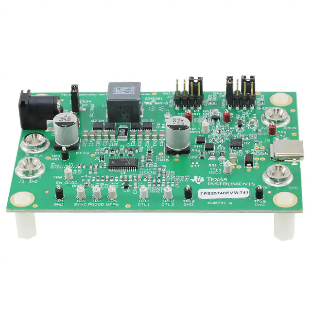


 工商网监
湘ICP备2023018690号
工商网监
湘ICP备2023018690号
