TPS40042
www.ti.com
SLUS777 – NOVEMBER 2007
LOW PIN COUNT, LOW VIN (3.0 V TO 5.5 V) SYNCHRONOUS BUCK DC-TO-DC
CONTROLLER WITH EXTERNAL REFERENCE INPUT
FEATURES
1
•
•
•
•
•
•
•
2
•
•
•
•
•
CONTENTS
3.0-V to 5.5-V Input
External Reference required: 0.5 V to 1.5 V
Output Voltage from REFIN to 90% of VIN
High-Side Drive for N-Channel FET
Supports Pre-Biased Outputs
Adaptive Anti-Cross Conduction Gate Drive
Fixed switching frequency (600 kHz) Voltage
Mode Control
Three Selectable Short Circuit Protection
Levels
Hiccup Restart from Faults
Active Low Enable
Thermal Shutdown Protection at 145°C
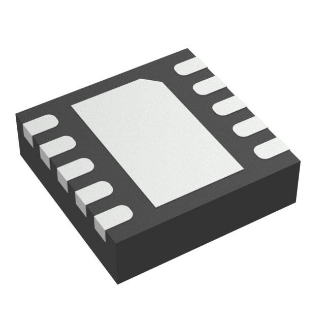
10-Pin, 3-mm x 3-mm SON (DRC)
2
Electrical Characteristics
4
Device Information
8
Application Information
10
Design Examples
18
Additional References
28
DESCRIPTION
The TPS40042 DC/DC controller is designed to
operate with an input source between a 3.0 V and 5.5
V. To reduce the number of external components, a
number of operating parameters are fixed internally.
The operating frequency for example, is internally set
at 600 kHz. (Continued)
APPLICATIONS
•
•
•
•
Device Ratings
DDR Memory
Point of Load
Telecommunications
DC to DC Modules
VIN
TPS40042
Reference Input
1
REFIN
2
EN
SW
9
3
FB
BOOT
8
4
COMP
LDRV
7
5
VDD
GND
6
HDRV 10
VOUT
Enable
UDG-07141
1
2
Please be aware that an important notice concerning availability, standard warranty, and use in critical applications of
Texas Instruments semiconductor products and disclaimers thereto appears at the end of this data sheet.
Predictive Gate Drive is a registered trademark of Texas Instruments.
PRODUCTION DATA information is current as of publication date.
Products conform to specifications per the terms of the Texas
Instruments standard warranty. Production processing does not
necessarily include testing of all parameters.
Copyright © 2007, Texas Instruments Incorporated
�TPS40042
www.ti.com
SLUS777 – NOVEMBER 2007
DESCRIPTION (CONT.)
One of three short circuit threshold levels may be selected by the addition of an external resistor from the COMP
pin to circuit ground (no resistor is the default setting). During power on, and before the internal soft start
commands the output voltage to rise, the TPS40042 enters a calibration cycle, measures the current out of the
COMP pin, and selects an internal SCP threshold voltage. At the end of the 1.5-ms calibration time, the output
voltage is allowed to enter soft-start. During operation, the selected SCP threshold voltage is compared to the
upper MOSFET’s voltage drop during its ON time to determine whether there is an overload condition. If the
voltage across the MOSFET exceeds the threshold voltage, the TPS40042 counts seven continuous pulses
before shutting completely OFF for seven soft start charge/discharge cycles, after which, the TPS40042 attempts
to restart the output.
During startup, both the high-side MOSFET switch and the synchronous rectifier are held in the OFF state until
the internal soft start commands an output voltage higher than the voltage currently at the output. This may
happen when the output is pre-biased at some voltage greater than zero and less than the desired regulation
voltage. When the internal soft start first commands the output to rise, the pulse width of the synchronous
rectifier is slowly increased from zero to the full 1-D conduction time by a number of discrete steps. In this way,
inductor current is not allowed to reverse quickly, and ensures a monotonic startup of the output whether the
output starts from zero or from a pre-bias level. If power is applied to the device while the EN (enable low) pin is
allowed to float high, the TPS40042 remains OFF. Only when the EN pin is pulled down towards ground is the
controller allowed to start.
ORDERING INFORMATION
OPERATING FREQUENCY
PACKAGE
TAPE AND REEL QTY.
PART NUMBER
600 kHz
Plastic 10-pin SON (DRC)
250
TPS40042DRCT
600 kHz
Plastic 10-pin SON (DRC)
3000
TPS40042DRCR
DEVICE RATINGS
ABSOLUTE MAXIMUM RATINGS
Over operating free-air temperature range (unless otherwise noted, all voltages are with respect to GND.)
PARAMETER
VALUE
VDD
UNIT
6.5
SW
-3 to 10.5
SW
transient (< 50 ns)
-5
BOOT
SW+6.5
HDRV
SW to SW+6.5
EN, FB, LDRV
,REFIN
V
-0.3 to 6.5
COMP
-0.3 to 3
Operating junction temperature
-40 to 150
Storage junction temperature
-55 to 150
°C
RECOMMENDED OPERATING CONDITIONS
over operating free-air temperature range (unless otherwise noted)
MAX
UNIT
VVDD
Input voltage to VDD pin
PARAMETER
MIN
3.0
5.5
V
VREFIN
Voltage applied to REFIN pin during regulation
0.5
1.5
V
TJ
Junction temperature
-40
125
°C
2
TYP
Copyright © 2007, Texas Instruments Incorporated
Product Folder Link(s): TPS40042
�TPS40042
www.ti.com
SLUS777 – NOVEMBER 2007
ELECTROSTATIC DISCHARGE (ESD) PROTECTION
PARAMETER
MIN
TYP
MAX
UNIT
Human body model
2500
V
CDM
1500
V
PACKAGE DISSIPATION RATINGS (1)
(1)
THERMAL IMPEDANCE
JUNCTION-TO-AMBIENT
TA = 25°C POWER RATING
TA = 85°C POWER RATING
48°C/W
2W
0.8W
For more information on the DRC package and the test method, refer to TI technical brief, literature number SZZA017.
3
Copyright © 2007, Texas Instruments Incorporated
Product Folder Link(s): TPS40042
�TPS40042
www.ti.com
SLUS777 – NOVEMBER 2007
ELECTRICAL CHARACTERISTICS
TJ = -40 °C to 85°C VVDD = 5 V, (unless otherwise noted)
PARAMETER
TEST CONDITIONS
MIN
TYP
MAX
UNIT
INPUT SUPPLY
VVDD
Input voltage range (1)
IDDsd
Shutdown
VEN = VVDD
IDDq
Quiescent
VFB = 0.8 V
IDDs
Switching current
No load at HDRV/LDRV
3.0
UVLOON
Minimum turn-on voltage
UVLOHYS
Hysteresis
3.0
5.5
V
100
180
µA
1.0
2.0
mA
1.90
2.05
2.2
V
80
130
200
mV
OSCILLATOR/ RAMP GENERATOR
fPWM
PWM frequency
3.0 V < VVDD < 5.5 V
500
600
700
kHz
fPWM
PWM frequency
VVDD = 5.0 V, 0°C < TJ < 70°C
540
600
660
kHz
VRAMP
Ramp amplitude PP
VPEAK – VVALLEY
0.75
0.87
1.0
V
VVALLEY
Ramp valley voltage
0.4
V
PWM
MAXDUTY Maximum duty cycle,
MINDUTY
Minimum duty cycle
MIN pulse
width (2)
Minimum controllable pulse width
VFB = 0 V, 3.0 V < VVDD < 5.5 V
88%
95%
0%
Minimum width control range before
jumping to zero.
90
150
ns
0
5
mV
-30
-125
nA
ERROR AMPLIFIER
VOS
FB to REFIN offset voltage
IFB
FB, REFIN input bias current
0.5 V < VREFIN < 1.5 V
-5
VOH
High level output voltage
IOH = 0.5 mA, VFB = 0 V, VVDD = 5.5
V
VOL
Low level output voltage
IOL = 0.5 mA, VFB = VVDD
IOH
Output source current
VCOMP = 0.7 V, VFB = GND
1
6
IOL
Output sink current
VCOMP = 0.7 V, VFB = VVDD
2
8
Gain bandwidth
5
10
MHz
Open loop gain
55
85
dB
GBW
(2)
AOL
2.0
2.5
80
V
150
mV
mA
SHORT CIRCUIT PROTECTION
TH1
Low short circuit threshold voltage
Resistor COMP to GND = 2.4 kΩ, TJ
= 25°C
80
105
130
VTH2
Medium short circuit threshold
voltage
Default: No resistor COMP to GND,
TJ = 25°C
140
175
210
VTH3
High short circuit threshold voltage
Resistor COMP to GND = 12 kΩ, TJ
= 25°C
250
310
370
(2)
Threshold temperature coefficient
3100
(2)
Minimum HDRV pulse time in over
current
190
tSWOCblank
(2)
SW leading edge blanking pulse in
over current detection
100
tHICCUP
Hiccup time between restarts
VTH(tc)
tON(oc)
(1)
(2)
mV
ppm
ns
40
ms
VVDD operation to 2.25 V is possible with some degradation in specifications. Under this condition, the VREFIN range is limited to 0.5 V to
0.7 V.
Ensured by design. Not production tested.
4
Copyright © 2007, Texas Instruments Incorporated
Product Folder Link(s): TPS40042
�TPS40042
www.ti.com
SLUS777 – NOVEMBER 2007
ELECTRICAL CHARACTERISTICS (continued)
TJ = -40 °C to 85°C VVDD = 5 V, (unless otherwise noted)
PARAMETER
TEST CONDITIONS
MIN
TYP
MAX
UNIT
SOFT START/ENABLE
tCAL (3)
Calibration time before softstart
begins
tSS (3)
Soft start time (4)
tREG
1.0
1.6
2.5
FB rise time from 0 V to VREFIN = 1.5
V
4.5
6.0
7.5
Time to voltage regulation
Sum of tCAL plus tSS ; VREFIN = 1.5 V
5.5
7.6
10
VEN
Enable threshold
EN voltage w.r.t. VVDD
-0.8
-1.2
-1.6
VENHYS
Enable hysteresis
50
ms
V
mV
BOOTSTRAP
RBOOT3V3
RBOOT5V
Bootstrap switch resistances
VBOOT to VVDD, VVDD = 3.3 V
50
VBOOT to VVDD, VVDD = 5 V
30
Ω
OUTPUT DRIVER
RHDHI3V3
HDRV pull-up resistance
VBOOT - VSW = 3.3 V, ISRCE = 100
mA
3.0
RHDLO3V3
HDRV pull-down resistance
VBOOT - VSW = 3.3 V, ISINK = 100 mA
1.5
3
RLDHI3V3
LDRV pull-up resistance
VVDD = 3.3 V, ISOURCE = 100 mA
3.0
5.5
RLDLO3V3
LDRV pull-down resistance
VVDD = 3.3 V, ISINK = 100 mA
1.0
2.0
tRISE (5)
LDRV, HDRV rise time
CLOAD = 1 nF
15
35
LDRV, HDRV fall time
CLOAD = 1 nF
10
25
TDEAD HL
Adaptive timing HDRV to LDRV
No load
15
30
45
TDEAD LH
Adaptive timing LDRV to HDRV
No load
5
15
35
tFALL
(5)
5.5
Ω
ns
SWITCH NODE
ILEAK
Leakage current
VEN = VVDD
µA
-2
THERMAL SHUTDOWN
tSD
(5)
Shutdown temperature
145
Hysteresis
(3)
(4)
(5)
15
°C
tCAL and tSS track with temperature and input voltage
Soft start time is a function of VREFIN. See Applications section for further detail.
Ensured by design. Not production tested.
5
Copyright © 2007, Texas Instruments Incorporated
Product Folder Link(s): TPS40042
�TPS40042
www.ti.com
SLUS777 – NOVEMBER 2007
TYPICAL CHARACTERISTICS
Quiescent Current (Non-Switching)
Shutdown Current
1.100
110
1.000
105
VDD = 5.5 V
100
IDDsd − µA
0.900
IDDq − mA
VDD = 2.25 V
0.800
0.700
95
90
85
0.600
80
0.500
VDD = 2.25 V
0.400
−40 −20
VDD = 5.5 V
75
70
0
20
40 60
80
Temperature − C
100 120
−40 −20
0
20
40 60
80
Temperature − C
Figure 1.
Figure 2.
UVLO Threshold
EN Threshold
−0.8
2.200
Turn ON
Turn OFF
Enable Threshold Relative to VDD − V
UVLO Threshold − V
2.150
2.100
2.050
2.000
1.950
1.900
1.850
1.800
−40
100 120
VDD = 5 V
−0.9
−1.0
−1.1
−1.2
−1.3
−1.4
−1.5
−1.6
−20
0
20
40 60
80
Temperature − C
100 120
−40
−20
0
20
40 60
80
Temperature − C
Figure 3.
100 120
Figure 4.
Oscillator Frequency
Soft Start Time; VREFIN = 1.5 V
700
6.6
VDD = 2.25V
VDD = 3.9V
VDD = 5.5V
VDD = 5 V
6.5
tSS - Soft Start Time - ms
Frequency − KHz
650
600
550
6.4
6.3
6.2
6.1
500
−40
6.0
−20
0
20
40 60
80
Temperature − C
100 120
-40
-20
0
20
40
60
80
100
120
T - Temperature - °C
Figure 5.
Figure 6.
6
Copyright © 2007, Texas Instruments Incorporated
Product Folder Link(s): TPS40042
�TPS40042
www.ti.com
SLUS777 – NOVEMBER 2007
TYPICAL CHARACTERISTICS (continued)
PWM Gain
ILIM Threshold
450
6.1
RC = 2.5 kΩ
400
VDD = 5 V
6.0
RC = 12.5 kΩ
RC =nil
ILIM Threshold − mV
350
Gain
5.9
5.8
5.7
5.6
250
200
150
100
5.5
−40
300
50
−20
0
20
40 60
80
Temperature − C
100 120
−40
−20
0
Figure 7.
20
40 60
80
Temperature − C
100 120
Figure 8.
Bootstrap Switch Resistance
Minimum Controllable Pulse Width
100
80
VDD = 3.3 V
VDD = 5 V
95
70
Pulse Width − ns
Switch Resistance − Ω
90
60
50
40
85
80
75
70
30
65
VDD = 2.25 V
60
−40
20
−40
−20
0
20
40 60
80
Temperature − C
100 120
−20
0
Figure 9.
20
40 60
80
Temperature − C
100 120
Figure 10.
Maximum Duty Cycle
SW Node Leakage Current
100
0.00
VDD = 2.25 V
VDD = 5.5 V
−0.50
VDD = 5.5 V
98
−0.10
−0.15
ISW − µA
Duty Cycle − %
VDD = 5.5 V
96
−0.20
−0.25
−0.30
94
−0.35
−0.40
92
−0.45
90
−40
−20
0
20
40 60
80
Temperature − C
100 120
−0.50
−40
Figure 11.
−20
0
20
40 60
80
Temperature − C
100 120
Figure 12.
7
Copyright © 2007, Texas Instruments Incorporated
Product Folder Link(s): TPS40042
�TPS40042
www.ti.com
SLUS777 – NOVEMBER 2007
DEVICE INFORMATION
TERMINAL CONFIGURATION
The package is an 10-pin SON (DRC) package.
1
REFIN
2
EN
SW
9
3
FB
BOOT
8
4
COMP
LDRV
7
5
VDD
GND
6
HDRV 10
Figure 13. DRC Package Terminal Configuration (Top View)
Table 1. TERMINAL FUNCTIONS
TERMINAL
NAME
BOOT
COMP
NO.
8
4
I/O
DESCRIPTION
I
Input (bootstrapped) supply to the high-side gate driver for PWM enabling the gate of the
high side FET to be driven above the input supply rail. Connect a ceramic capacitor from this
pin to SW. This capacitor is charged from the VDD pin voltage through an internal switch.
The switch is turned ON during the off time of the converter. To slow down the turn on of the
external MOSFET, a small resistor (1 Ω to 3 Ω) may be placed in series with the bootstrap
capacitor. See Applications Section to calculate the appropriate value.
O
Output of the error amplifier and connection node for loop feedback components. The
voltage at this pin determines the duty cycle for the PWM. Optionally, a resistor from this pin
to ground is used to determine the voltage threshold used for short circuit protection. (See
Application Section)
• Low threshold R = 2.4 kΩ, ±10%
• Mid threshold R = not installed
• High threshold R = 12 kΩ, ±10%
EN
2
I
Active low enable input allows ON/OFF operation of the controller. If power is applied to the
TPS40042 while the EN pin is allowed to float high, the TPS40042 remains disabled (both
external switches are held OFF). Only when the EN pin is pulled to 1.2 V below VDD is the
TPS40042 allowed to start. An internal 100-kΩ resistor is connected between VDD and EN
to provide pull up. Connect this pin to GND to bypass the enable function.
FB
3
I
Inverting input of the error amplifier. In closed loop operation, the voltage at this pin is at the
same potential as the REFIN pin. A series resistor divider from the converter output to
ground, with the center connection tied to this pin, determines the value of the regulated
output voltage. This pin is also a connection node for loop feedback components.
GND
6
HDRV
10
O
This is the gate drive output for the high side N-channel MOSFET switch for PWM. It is
referenced to SW and is bootstrapped for enhancement of the high-side switch.
LDRV
7
O
Gate drive output for the low-side synchronous rectifier (SR) N-channel MOSFET.
REFIN
1
I
Non-inverting imput to the error amplifier. A precision voltage must be applied to this pin
before the TPS40042 is enabled. Since this input is connected directly to the non-inverting
pin of the error amplifier, the quality of the voltage at this pin has a direct impact on the
quality of the output voltage.
Electrical ground connection for the device.
SW
9
O
Connection to the switched node of the converter and the power return for the upper gate
driver. There should be a high current return path from the source of the upper MOSFET to
this pin. It is also used by the adaptive gate drive circuits to minimize the dead time between
upper and lower MOSFET conduction.
VDD
5
I
Power input to the device. This pin should be locally bypassed to GND with a low ESR
ceramic capacitor of 1 µF or greater.
PPAD
Thermal pad used to conduct heat from the device. This pad should be tied externally to a
ground plane. See Application Section for PC board layout information.
8
Copyright © 2007, Texas Instruments Incorporated
Product Folder Link(s): TPS40042
�TPS40042
www.ti.com
SLUS777 – NOVEMBER 2007
Block Diagram
TPS40042
VDD
5
100 kW 2 V
EN
VDD/2
VDD
UVLO
SW
SDN
EN
100-ns
Delay
Fault
Logic
2
ILIMSET
VDD
Current Limit
Comparator
(VDD- 1.2 V)
REFIN
LDRV
1
SDN
CLK
8
FB
PWM
Comparator
+
+
Soft
Start
HI
Adaptive
Gate
Drive
Ramp
COMP
4
0.6 V
VREF
Reference
9
SW
7
LDRV
VDD
Oscillator
VDD
10 HDRV
PWM
Logic
3
BOOT
LO
ILIMSET
Calibration
Circuit
(one of three levels)
Thermal
Shutdown
Pre-Bias
6
UDG-07139
GND
Figure 14. Functional Block Diagram
9
Copyright © 2007, Texas Instruments Incorporated
Product Folder Link(s): TPS40042
�TPS40042
www.ti.com
SLUS777 – NOVEMBER 2007
APPLICATION INFORMATION
Functional Description
The TPS40042 is a fixed frequency voltage mode synchronous buck controller. In operation, the Synchronous
Rectifier (SR) is allowed to conduct current in both directions, allowing a converter to operate in continuous
cnduction (CCM) mode, even under no load conditions, simplifying feedback loop compensation requirements.
During startup, internal circuitry modulates the switching of the synchronous rectifier to prevent discharging of the
output if a pre-biased condition exists.
Voltage Reference Input
An external voltage reference input is required. During operation, the voltage must be between 0.5v and 1.5v.
REFIN may be used in either of two ways:
• As a reference input. In this case, REFIN must be stable before the TPS40042 is enabled. the internal
soft-start controls the rate of rise of the output voltage during startup. The time to reach output voltage
regulation is dependent on the voltage on the REFIN pin.
• As a tracking input. If REFIN is held to zero until soft-start has completed (7.6-ms), then REFIN will control
the output voltage during startup and regulation.
Voltage Error Amplifier
The error amplifier has a bandwidth of greater than 5 MHz, and open loop gain of at least 55 dB. The output
voltage swing is limited to just above and below the oscillator ramp levels to improve transient response.
Loop Compensation
Voltage mode buck type converters are typically compensated using Type III networks. Please refer to the
Design Example for detailed methodology in designing feedback loops for voltage mode converters.
DESIGN
HINT:
æ
-
t
When designing the compensation for the feedback loop, remember that a low
impedance compensation network combined with a long network time constant
can cause the short circuit threshold setting to not be as expected. The time
constant and impedance of the network connected from COMP to FB should be
as shown in Equation 1 to guarantee no interaction with the short circuit
threshold setting.
ö
ç
÷
0.4 V
R ´C
´ eè FB FB ø < 10 mA
RFB
(1)
where
•
•
t is 1 ms, the sampling time of the short circuit threshold setting circuit
RFB and CFB are the values of the feedback components. e.g. R3 and C4 of the Design Example.
Oscillator
The oscillator frequency is internally fixed. The TPS40042 operating frequencies is nominally 600 kHz.
UVLO
When the input voltage is below the UVLO threshold, the TPS40042 turns off the internal oscillator and holds all
gate drive outputs in the low (OFF) state. When the input rises above the UVLO threshold, and the EN pin is
below the turn ON threshold, the start-up sequence is allowed to begin.
10
Copyright © 2007, Texas Instruments Incorporated
Product Folder Link(s): TPS40042
�TPS40042
www.ti.com
SLUS777 – NOVEMBER 2007
Enable and Start-Up Sequence
The EN pin of the TPS40042 is internally pulled to VDD. When power is applied to VDD, the EN pin is allowed to
float high, and the TPS40042 remains OFF. Only when the EN pin is externally pulled below the threshold
voltage of (VVDD - 1.2 V) is the TPS40042 allowed to start. When enabled, the TPS40042 enters a calibration
cycle where the short circuit current threshold is determined. The TPS40042 monitors the current out of the
COMP pin and selects a threshold based on the sensed value of the current. See Selecting the Short Circuit
Current Limit Threshold section for for details. When this calibration time is completed, the soft-start cycle is
allowed to begin. See Figure 15 below.
EN
COMP
VOUT
Configure
ILIM
Threshold
Soft Start
1.6
6
T - Time - ms
Figure 15. Startup with VREFIN =1.5 V
DESIGN
HINT:
If the enable function is not used, the EN pin should be connected to ground
(GND).
DESIGN
HINT:
When designing the feedback loop compensation, ensure the capacitors used
are not so large that they distort the COMP pin calibration waveform.
Soft Start
At the end of a calibration cycle, the TPS40042 slowly increases the voltage to the non-inverting input of the
error amplifier. In this way, the output voltage slowly ramps up until the voltage on the non-inverting input to the
error amplifier reaches the external (VREFIN) reference voltage. At that time, the voltage at the non-inverting input
to the error amplifier remains at the applied reference voltage.
During the soft-start interval, pulse-by-pulse current limiting is active. If seven consecutive current limit pulses are
detected, overcurrent is declared and a timeout period equivalent to seven calibration/soft-start cycles goes into
effect. See Output Short Circuit Protection section for details.
Since the rate of rise of the output voltage is constant with different REFIN voltage levels, the actual soft start
time is directly proportional to the value of the external reference voltage. The rate of rise at the non-inverting
input of the error amplifier is 0.25 V/ms. The rate of rise measured at the output terminals of the DC/DC
converter will be increased by the output voltage-to-reference voltage ratio.
æV
ö
tSS = ç REFIN ÷ ´ 6.0ms
1.5
V
è
ø
(2)
For example, if a 1-V external reference is applied for a 1.5-V output DC/DC converter, the soft-start
time-to-output voltage regulation is 4 ms.
11
Copyright © 2007, Texas Instruments Incorporated
Product Folder Link(s): TPS40042
�TPS40042
www.ti.com
SLUS777 – NOVEMBER 2007
Pre-Bias Startup
The TPS40042 supports pre-biased output voltage applications. In cases where the output voltage is held up by
external means while the TPS40042 is off, full synchronous rectification is disabled during the initial phase of soft
starting the output voltage. When the first PWM pulses are detected during soft start, the controller slowly
initiates synshronous rectification by starting the synchronous rectifier with a narrow on time. It then increments
that on time on a cycle-by-cycle basis until it coincides with the time dictated by (1-D), where D is the duty cycle
of the converter. This approach prevents the sinking of current from a pre-biased output, and ensures the output
voltage startup and ramp to regulation is smooth and controlled.
NOTE:
If the output is pre-biased, PWM pulses start when the internal soft-start voltage rises
above the error amplifier input (FB pin).
Figure 16 below depicts the waveform of the HDRV and LDRV output signals at the beginning PWM pulses.
When HDRV turns off, diode rectification is enabled. Before the next PWM cycle starts, LDRV is turned on for a
short pulse. With every clock cycle, the leading edge of LDRV is modulated, increasing the on time of the
synchronous rectifier. Eventually, the leading edge of LDRV coincides with the falling edge of HDRV to achieve
full synchronous rectification. During normal operation of the converter, the TPS40042 operates in full two
quadrant source/sink mode.
Figure 17 shows the startup waveform of a 1.2-V output converter under three different pre-biased output
conditions. The lowest trace is when there is no pre-bias on the output. The center and top most traces indicate
converter startup with 0.5-V and 1.0-V pre-bias conditions.
VIN = 5 V
VOUT = 1.2 V
(200 mV/div)
PREBIAS = 1 V
VHDRV
PREBIAS = 0.5 V
PREBIAS = 0 V
VLDRV
t − Time − 2 µs/div
t − Time − 500 µs/div
Figure 16. MOSFET Drivers at Beginning of Soft Start
Figure 17. Startup Waveforms; VREFIN = 0.6 V
The recommended output voltage pre-bias range is less than or equal to 90% of the final regulation voltage. A
pre-biased output voltage of 90% to 100% of final regulation could lead to the sinking of current from the pre-bias
source. If the pre-biased voltage is greater than the designed converter output regulation voltage, then upon the
completion of the soft-start interval, the TPS40042 turns ON the Synchronous Rectifier, therby drawing current
from the output to bring the output voltage into regulation. Note that this may cause some undershoot of the
output voltage before entering regulation.
Output Short Circuit Protection
To minimize circuit losses, the TPS40042 uses the RDS(on) of the upper MOSFET switch as the current sensing
element. The current limit comparator, initially blanked during the first portion of each switching cycle, senses the
voltage across the high-side MOSFET when it is fully ON. This voltage is compared to an internally selected
short circuit current (SCC) limit threshold voltage. If the comparator senses a voltage drop across the high-side
MOSFET greater than the SCC limit threshold, it outputs an OC pulse. This terminates the current PWM pulse
12
Copyright © 2007, Texas Instruments Incorporated
Product Folder Link(s): TPS40042
�TPS40042
www.ti.com
SLUS777 – NOVEMBER 2007
preventing further current ramp-up, and sets the fault counter to count up one count on the next clock cycle.
Similarly, if no OC pulse is detected, the fault counter decrements by one count. If seven OC pulses are
summed, a fault condition is declared and the upper switch of the PWM output of the chip is immediately
disabled (turned OFF) and remains that way until the fault time-out period has elapsed. Both HDRV and LDRV
drivers are kept OFF during the fault time-out.
The fault time-out period is determined by cycling through seven internal soft-start time periods. At the end of the
fault time-out period, startup is attempted again.
The main purpose is for hard fault protection of the power switches. The internal SCC voltage has a positive
temperature coefficient designed to improve the short circuit threshold tolerance variation with temperature.
However, given the tolerance of the voltage thresholds and the RDS(on) range for a MOSFET, it is possible to
apply a load that thermally damages the external MOSFETs.
Selecting the Short Circuit Current Limit Threshold
The TPS40042 uses one of three user selectable voltage thresholds. During the calibration interval at power on
or enable (Figure 15), the TPS40042 monitors the current out of the COMP pin and selects a threshold based on
the sensed value. If the current is zero; that is, no resistor is connected between COMP and GND, then the
threshold voltage level is 180 mV. If a 2.4-kΩ resistor is connected between COMP and GND, then the threshold
voltage level is 105 mV. If a 12-kΩ resistor is connected between COMP and GND, then the threshold voltage is
310 mV.
Once calibration is complete, the selected SCP threshold level is latched into place and remains constant. In
addition, the sensing circuits on COMP pin during calibration are disconnected from the COMP pin, and soft start
is allowed to begin.
Synchronous Rectification and Gate Drive
In a buck converter, when the upper switch MOSFET turns off, current is flowing in the inductor to the load. This
current cannot be stopped immediately without using infinite voltage. To give this current a path to flow and
maintain voltage levels at a safe level, a rectifier or catch device is used. This device can be either a diode, or it
can be a controlled active device. The TPS40042 provides a signal to drive an N-channel MOSFET as a
synchronous rectifier (SR). This control signal is carefully coordinated with the drive signal for the main switch so
that there is minimum dead time from the time that the SR turns OFF and the upper switch MOSFET turns ON,
and minimum delay from when the upper switch MOSFET turns OFF and the SR turns ON.
NOTE:
The longer the time spent in diode conduction during the rectifier conduction period,
the lower the converter efficiency.
The drivers for the external HDRV and LDRV MOSFETs are capable of driving a gate to source voltage of
approximately 5 V. At VDD = 5 V, the drivers are capable of driving MOSFETs appropriate for a 15-A converter.
The LDRV driver switches between VDD and ground, while HDRV driver is referenced to SW and switches
between BOOT and SW. The drivers have non-overlapping timing that is governed by an adaptive delay circuit
that minimizes body diode conduction in the synchronous rectifier.
Gate Drive Resistors
The TPS40042’s adaptive gate delay circuitry monitors the HDRV-to-SW and LDRV-to-GND voltages to
determine the state of the external MOSFET switches. Any voltage drop across an external series gate drive
resistor is sensed as reduced gate voltage during turn-off and may interfere with the MOSFET timing.
DESIGN
HINT:
A resistor should never be placed in series with the synchronous rectifiers gate
and the gate trace should be kept as short as practical in the layout.
13
Copyright © 2007, Texas Instruments Incorporated
Product Folder Link(s): TPS40042
�TPS40042
www.ti.com
SLUS777 – NOVEMBER 2007
Total Gate Charge
The internal voltage sensing of the external MOSFET gate voltages used by the TPS40042 to control the
dead-times between turn-off and turn-on can be sensitive to large MOSFET gate charges, especially when
different gate charges are used for the high-side and low-side MOSFETs. Increased gate charge increases
MOSFET switching times and decreases the dead-time between the MOSFETs switching.
DESIGN
HINT:
MOSFETs with no more than 40 nC of total gate charge should be selected.
The upper switch MOSFET’s gate charge should be no less than 60% of the
synchronous rectifier’s gate charge to minimize the turn-on/turn-off delay
mismatch between the high-side and low-side MOSFET.
Synchronous Rectifier dV/dt Turn-On
As the upper switch MOSFET turns on, the switch node voltage rises from close to ground to VIN in a very short
period of time (typically 10 ns to 30 ns) resulting in very high voltage spikes on the switch node. The construction
of a MOSFET creates parasitic capacitances between its terminals, particularly the gate-to-drain and
gate-to-source, creating a capacitive divider between the drain and source of the MOSFET with the gate at its
mid-point. If the gate-to-drain charge (QGD) is larger than the gate-to-source charge (QGS), the capacitive divider
places proportionally more charge on the gate of the MOSFET as the switch node voltage rises than is shunted
to GND. In extreme cases, this can cause the synchronous rectifier gate voltage to rise above the turn on
threshold voltage of the MOSFET and causes cross-conduction. This is called dV/dt turn-on. It increases power
dissipation in both the high-side and the low-side MOSFET, reducing efficiency.
DESIGN
HINT:
Select a synchronous rectifier MOSFET with a QGD to QGS ratio of less than
one and provide a wide, low resistance, low inductance loop in the synchronous
rectifier gate drive circuit. (See Layout Consideration)
DESIGN
HINT:
A resistor in series with the boost capacitor slows the turn on of the high-side
MOSFET, and reduces the dV/dt of the switch node. See Boost Capacitor
Series Resistor section.
Bootstrap for N-Channel MOSFET Drive
The PWM duty cycle is limited to a maximum of 95%, allowing the bootstrap capacitor to charge during every
cycle. During each PWM OFF period, the voltage on VDD charges the bootstrap capacitor. When the PWM
switch is next commanded to turn ON, the voltage used to drive the MOSFET is derived from the voltage on this
capacitor. Since this is a charge transfer circuit, the value of the bootstrap capacitor must be sized such that the
energy stored in the capacitor on a per cycle basis is greater then the gate charge requirement of the MOSFET
being used. See the Design Example section for details.
Bootstrap Capacitor Series Resistor
Since resistors should not be placed in series with the high-side gate, it may be necessary to place a small 1-Ω
to 3-Ω resistor in series with the bootstrap capacitor to control the turn-on of the main switching MOSFET and
reduce the dV/dt rate of rise of the switch node voltage. A resistor placed between the BOOT pin and the
bootstrap capacitor increases the series resistance during the turn-on of the high-side MOSFET, and has no
effect during the high-side MOSFET’s turn-off period. This prevents the TPS40042 from sensing the upper switch
MOSFET’s turn-off too early and reducing the upper switch MOSFET turn-off to the SR MOSFET turn-on delay
timing too far.
DESIGN
HINT:
To reduce EMI, place a small 1-Ω to 3-Ω resistor in series with the boost
capacitor to control the turn-on of the main switching FET.
External Schottky Diode for Low Input Voltage
The TPS40042 uses an internal P-channel MOSFET switch between VDD and BOOT to charge the bootstrap
capacitor during synchronous rectifier conduction time. At low input voltages, a MOSFET can not be turned on
14
Copyright © 2007, Texas Instruments Incorporated
Product Folder Link(s): TPS40042
�TPS40042
www.ti.com
SLUS777 – NOVEMBER 2007
hard enough to rapidly replenish the charge required to turn on an (high gate charge) external high-side
MOSFET. For this situation, an external Schottky diode between the VDD and BOOT pins may be added. While
the diode carries very small average current (QG x FSW) it may be required to carry several hundred mA of peak
surge current. The diode should be rated for at least 500 mA of surge current. For higher input voltage
applications, if a resistor is used in series with the boost capacitor, connect the diode to the junction of the
resistor and capacitor to remove the added resistance from the capacitor’s charge path.
DESIGN
HINT:
For low input voltages, and a high gate charge upper switch MOSFET, a small
Schottky diode should be placed from VDD to BOOT. Do not use a resistor in
series with the boost capacitor.
VDD Bypass and Filtering
To prevent switching noise from being injected into the TPS40042 control circuitry, a ceramic capacitor (1 µF
minimum) must be placed as close to the VDD pin and GND pad as possible.
VDD Filter Resistor
To further limit the noise on VDD, a small 1-Ω to 2-Ω resistor may be placed between the input voltage and the
VDD pin to create a small filter to VDD. The resistor should connect near the drain of the upper switch MOSFET
to prevent trace IR drops from increasing the sensed voltage drop. The resistor itself should be placed close to
Pin 5.
The current through the resistor includes the device's no-load switching current of 2 mA plus gate switching
current. The voltage drop induced across this resistor reduces the VDD-to-SW voltage sensed by the over
current protection circuitry within the device. This results with the apparent voltage drop across the upper switch
MOSFET being increased, thereby decreasing the current at which protection will occur. To minimize this effect,
the resistor value should be selected to yield less than a 25-mV drop.
Thermal Shutdown
If the junction temperature of the device reaches the thermal shutdown level, the PWM and the oscillator are
turned off and HDRV and LDRV are driven off. When the junction cools to the required level, the PWM soft starts
as during a normal power-up cycle.
Package Power Dissipation
The power dissipation in a controller is largely dependent on the MOSFET driver currents and the input voltage.
The driver current is proportional to the total gate charge, Qg, of the external MOSFETs, and the operating
frequency of the converter. The total power dissipation is:
(
)
PT = VDD ´ Iq + fSW ´ (QSW + QSR )
(3)
where
•
•
•
IQ is the quiescent operating current (neglecting drivers)
QgSWis the total gate charges of the upper switch MOSFET
QgSR is the total gate charges of the synchronous rectifier MOSFET
The maximum power capability of the PowerPad™ package is dependent on the layout as well as air flow. The
thermal impedance from junction-to-air assuming 2-oz. copper trace and thermal pad with solder and no air flow
is detailed in Reference [5].
15
Copyright © 2007, Texas Instruments Incorporated
Product Folder Link(s): TPS40042
�TPS40042
www.ti.com
SLUS777 – NOVEMBER 2007
PCB Layout Guidelines
A synchronous BUCK power stage has two primary current loops, the input current loop that carries high ac
discontinuous current and an output current loop that carries high dc continuous current. The output current loop
carries low ac inductor ripple current.
V IN
VDD Filter
(Optional)
Main
Gate
Drive
TPS40042
Reference
Input
REFIN
EN
Input
Current
Loop
HDRV
EN
SW
FB
BOOT
VOUT
Enable Bypass
(Optional)
BOOST Resistor
(Optional)
COMP
VDD
Bypass
Output
Current
Loop
LDRV
SR Gate
Drive
GND
VDD
PPAD
Current
Limit Set
Resistor
SignalGround
PowerGround Locate Components OverPower Ground
UDG-07140
Locate Components Over SignalGround Island
Figure 18. Synchronous BUCK Power Stage
Power Component Routing
As shown in Figure 18, the input current loop contains the input capacitors, the switching MOSFET, the inductor,
the output capacitors, and the ground path back to the input capacitors. To keep this loop as small as possible, it
is good practice to place some ceramic capacitance directly between the drain of the main switching MOSFET
and the source of the synchronous rectifier (SR) through a power ground plane directly under the MOSFETs.
The output current loop includes the filter inductor, the output capacitors, and the ground return between the
output capacitors and the source of the synchronous rectifier MOSFET. As with the input current loop, the ground
return between the output capacitor ground and the source of the SR source should be routed under the inductor
and MOSFETs to minimize the power loop area.
Device to Power Stage Interface
The TPS40042 uses a very fast break-before-make anti-cross conduction circuit to minimize power loss. Adding
external impedance in series with the gates of the switching MOSFETs adversely affects the converter’s
operation and must be avoided. The loop impedance (HDRV-to-gate plus source-to-SW and LDRV-to-SR gate
plus SR source-to-GND) should be kept to less than 20 nH to avoid possible cross-conduction. The HDRV and
LDRV connections should widen to 20 mils as soon as possible out from the device pin.
The return for the main switching MOSFET gate drive is the SW pin of the TPS40042. The SW pin should be
routed to the source of the main switching FET with at least a 20-mils wide trace as close to the HDRV trace as
possible to minimize loop impedance.
The return for the SR MOSFET gate drive is the TPS40042 GND pad. The GND pad should be connected
directly to the source of the SR with at least a 20-mil wide trace directly under the LDRV trace. Use a minimum of
2 parallel vias to connect the GND pad to the source of the SR if multiple layers are used.
16
Copyright © 2007, Texas Instruments Incorporated
Product Folder Link(s): TPS40042
�TPS40042
www.ti.com
SLUS777 – NOVEMBER 2007
A small, less than 3-Ω resistor may be added in series with the BOOT pin to slow the turn-on of the upper switch
MOSFET, thereby reducing the rising edge slew-rate of the switch node. In turn, this reduces EMI, increases
upper MOSFET OFF to SR ON dead time, and minimizes induced dV/dt turn-on of the SR when the upper switch
MOSFET turns on. It is recommended customers make provisions on their boards for this resistor and not use
resistors in series with MOSFET gate leads.
VDD Filtering
A ceramic capacitor, 1 µF minimum, must be placed as close to the VDD pin and GND pad as possible with a
15-mil wide (or greater) trace. If used, a small series connected resistor (1 Ω to 2 Ω) may be placed less than
100 mils from the TPS40042 between the supply input voltage and the VDD pin to further reduce switching noise
on the VDD pin.
NOTE:
The voltage drop across this resistor affects the level at which the over-current circuit
operates by filtering the sensed VDD voltage.
Device Connections
If a current limit resistor is used (COMP to GND), it must be placed within 100 mils of the COMP pin to limit noise
injection into the PWM comparator. Compensation components (feedback divider, and associated error amplifier
components) should be placed over a signal ground island connected to the power ground at the GND pad
through a 10-mil wide trace. If multiple layers are used, connect to GND through a single via on an internal layer
opposite the connection to the source of the synchronous rectifier.
PowerPAD™ Layout
The PowerPAD™ package provides low thermal impedance for heat removal from the device. The PowerPAD™
derives its name and low thermal impedance from the large bonding pad on the bottom of the device. The circuit
board must have an area of solder-tinned-copper underneath the package. The dimensions of this area depend
on the size of the PowerPAD™ package. See PCB Layout Guidelines for further information.
Thermal vias connect this area to internal or external copper planes and should have a drill diameter sufficiently
small so that the via hole is effectively plugged when the barrel of the via is plated with copper. This plug is
needed to prevent wicking the solder away from the interface between the package body and the solder-tinned
area under the device during solder reflow. Drill diameters of 0.33 mm (13 mils) works well when 1-oz copper is
plated at the surface of the board while simultaneously plating the barrel of the via. If the thermal vias are not
plugged when the copper plating is performed, then a solder mask material should be used to cap the vias with a
diameter equal to the via diameter plus 0.1 mm minimum. This capping prevents the solder from being wicked
through the thermal vias and potentially creating a solder void under the package. Refer to PowerPAD™
Thermally Enhanced Package[2] for more information on the PowerPAD™ package.
17
Copyright © 2007, Texas Instruments Incorporated
Product Folder Link(s): TPS40042
�TPS40042
www.ti.com
SLUS777 – NOVEMBER 2007
DESIGN EXAMPLES
Example 1. A 5-V to 1.8-V DC-to-DC Converter Using a TPS40042
The following example illustrates the design process and component selection for a 5-V to 0.9-V DDR
termination synchronous buck converter. The design goal parameters are given in the table below. A list of
symbol definitions is found at the end of this section.
Design Goal Parameters
SYMBOL
PARAMETER
TEST CONDITION
MIN
TYP
MAX
VIN
Input voltage
VINripple
Input ripple
IOUT = 6 A
4.5
VOUT
Output voltage
IOUT = 0 A, VIN = 5 V
Line regulation
VIN = 4.5 A to 5.5 V
0.5%
0.5%
Load regulation
IOUT = 0 A to 6 A
VRIPPLE
Output ripple
IOUT = 6 A
VTRANS
Transient deviation
IOUT = -2 A to 2 A, IOUT = 2 A to -2 A
IOUT
Output current
VIN = 4.5 V to 5.5 V
FSW
Switching frequency
UNIT
5.5
V
75
mV
0.9
V
36
mV
40
-6
6
600
Size
A
kHz
1
In2
For this example, the schematic shown in Figure 19 is used.
Figure 19. TPS40042 Sample Schematic
Inductor Selection
The inductor is typically sized for 30% peak-to-peak ripple current (IRIPPLE) Given this target ripple current, the
required inductor size is calculated by:
18
Copyright © 2007, Texas Instruments Incorporated
Product Folder Link(s): TPS40042
�TPS40042
www.ti.com
L+
SLUS777 – NOVEMBER 2007
V IN(max) * V OUT
0.3
I OUT
VOUT
V IN(max)
1
F SW
(4)
Solving with VIN(max) = 5.5 V, an inductor value of 0.69 µH is obtained. A standard value of 0.8 µH is selected,
resulting in 1.56-A peak-peak ripple. The RMS current through the inductor is approximated by the equation:
I L(rms) +
Ǹǒ
2
2
I L(avg)Ǔ ) 1 ǒI RIPPLEǓ +
12
ǸǒI
Ǔ
OUT
2
2
) 1 ǒI RIPPLEǓ
12
(5)
Using Equation 5, the maximum RMS current in the inductor is about 6 A.
Output Capacitor Selection (C8 & C9)
The selection of the output capacitor is typically driven by the output load transient response requirement.
Equation 6 and Equation 7 estimate the output capacitance required for a given output voltage transient
deviation.
ITRAN(max)2 ´ L
C OUT(min) =
(VIN(min) - VOUT )´ VTRAN ´ 2
COUT(min) =
ITRAN(max)2 ´ L
VOUT ´ VTRAN ´ 2
when VIN(min) < 2 ´ VOUT
(6)
when VIN(min) > 2 ´ VOUT
(7)
For this example, Equation 7 is used in calculating the minimum output capacitance.
Based on a 4-A load transient with a maximum 40-mV deviation, a minimum of 177-µF output of capacitance is
required.
The output ripple is divided into two components. The first is the ripple voltage generated by inductor ripple
current flowing through the output capacitor's capacitance, and the second is the voltage generated by the ripple
current flowing in the output capacitor's ESR. The maximum allowable ESR is then determined by the maximum
ripple voltage and is approximated by:
ESR MAX +
VRIPPLE(total) * VRIPPLE(cap)
I RIPPLE
V RIPPLE(total) *
+
ǒ
Ǔ
I RIPPLE
C OUT F SW
I RIPPLE
(8)
Based on 177 µF of capacitance, 1.56-A ripple current, 600-kHz switching frequency and a design goal of 36-mV
ripple voltage, we calculate a maximum ESR of 13.6 mΩ. Two 1206, 100-µF, 6.3-V, X5R ceramic capacitors are
selected to provide significantly less than 13.6 mΩ of ESR.
Peak Current Rating of Inductor
With output capacitance known, it is now possible to calculate the charging current during start-up and determine
the minimum saturation current rating for the inductor. The start-up charging current is approximated by:
V
COUT
I CHARGE + OUT
T SS
(9)
Using the TPS40042’s soft-start time of 5-ms, COUT = 200 µF and VOUT = 0.9 V, ICHARGE is found to be 40 mA.
The peak current rating of the inductor is now found by:
L L(peak) + I OUT(max) ) 1 ǒI RIPPLEǓ ) I CHARGE
2
(10)
The inductor requirements are summarized in the table below.
19
Copyright © 2007, Texas Instruments Incorporated
Product Folder Link(s): TPS40042
�TPS40042
www.ti.com
SLUS777 – NOVEMBER 2007
Inductor Requirements
PARAMETER
Inductance
RMS current (thermal rating)
Peak current (saturation rating)
SYMBOL
VALUE
UNITS
L
0.8
µH
IL(rms)
6.0
A
IL(peak)
7.08
A PG0083.801, 0.8 µH is selected for its small size, low DCR and high current handling capability.
Input Capacitor Selection (C1 & C2)
The input voltage ripple is divided between capacitance and ESR. For this design, VRIPPLE(CAP) = 50 mV and
VRIPPLE(ESR) = 25 mV. The minimum capacitance and maximum ESR are estimated by:
I LOAD VOUT
C IN(min) +
VRIPPLE(cap) VIN F SW
(11)
ESR MAX +
VRIPPLE(ESR)
I LOAD ) 1 ǒI RIPPLEǓ
2
(12)
For this design, CIN > 60 µF and ESR < 3.5 mΩ. The RMS current in the input capacitors is estimated by:
I RMS(cin) + I IN(rms) * I IN(avg) +
Ǹƪǒ
2
2
I OUTǓ ) 1 ǒI RIPPLEǓ
12
ƫ
VOUT V OUT I OUT
*
V IN
V IN
(13)
With VIN = VIN(max), the input capacitors must support a ripple current of 1.56 ARMS. Two 1206, 100-µF, X5R
ceramic capacitors with about 2-mΩ ESR and a 2-A RMS current rating are selected. It is important to check the
dc bias voltage derating curves to ensure the capacitors provide sufficient capacitance at the working voltage.
MOSFET Switch Selection (Q1 & Q2)
The switching losses for the upper switch MOSFET are estimated by:
P G1SW + 1
2
V IN
I OUT
ǒT RISE ) T FALLǓ
F SW + V IN
I OUT
Q GS2_Q1 ) Q GD_Q1
VDD*V TH
R DRIVE
F SW
(14)
For this design, switching losses are higher at low input voltage due to the lower gate drive current. Designing for
1 W of total losses in both MOSFETS and 20% of the total MOSFET losses in switching losses, we can estimate
our maximum gate-to-drain charge for the design at:
PG1SW
V DD * V t
1
Q GS2_Q1 ) Q GD_Q1 t
VIN I OUT
R DRIVE
F SW
(15)
For a low-gate threshold MOSFET, and the TPS40042’s 5 Ω and 3 Ω drive resistances, we estimate a maximum
QGS2+QGD of 10.8 nC.
The conduction losses in the upper switch MOSFET are estimated by the RMS current through the MOSFET
times its RDS(on):
2
2
V
2
ǒI OUTǓ ) 1 ǒIRIPPLEǓ
P CON_Q1 + D
RDS(on) + OUT I L(rms)
R DS(on_Q1)
12
VIN
ƪ
ƫ
(16)
Estimating about 30% of total MOSFET losses to be high-side conduction losses, the maximum RDS(on) of the
high-side MOSFET can be estimated by:
P CON_Q1
R DS(on_Q1) +
V OUT
2
I L(rms)
VIN
(17)
For this design, with IL_RMS = 6 ARMS and 4.5 V to 0.9 V, RDS(on_Q1) is < 39 mΩ for the upper switch MOSFET.
20
Copyright © 2007, Texas Instruments Incorporated
Product Folder Link(s): TPS40042
�TPS40042
www.ti.com
SLUS777 – NOVEMBER 2007
Estimating 50% of total MOSFET losses are in the SR as conduction losses, repeat equation 14. Then calculate
the maximum RDS(on) of the SR by the equation:
PCON_Q2
R DS(on_Q2) +
V
2
I L(rms)
1 * OUT
V IN
ǒ
Ǔ
(18)
For this design IL_RMS = 6 A at 5.5 V to 0.9 V RDS(on_Q2) < 15.9 mΩ. The table below summarizes the MOSFET
requirements.
MOSFET Requirements
PARAMETER
SYMBOL
High-side FET RDS(on)
High-side FET turn-on charge
Low-side FET RDS(on)
VALUE
UNITS
RDS(on_Q1)
39
mΩ
QGS2_Q1 +QGD_Q1
10.8
nC
RDS(on_Q2)
15.9
mΩ
IRF7910 has an RDSON(max) of 15 mΩ at 4.5-V gate drive,QGD of 6.2 nC, and QGS2 of 2 nC.
Bootstrap Capacitor (C7)
To ensure proper charging of the upper switch MOSFET gate, limit the ripple voltage on the bootstrap capacitor
to < 5% of the minimum gate drive voltage of 3.0 V.
20 Q GS_Q1
C BOOST +
V IN(min)
(19)
Based on the IRF7910 MOSFET with a maximum total gate charge of 26 nC, calculate a minimum of 116 nF of
capacitance. The next higher standard value of 220 nF is selected.
VDD Bypass Capacitor (C6)
Select a 1.0-µF ceramic bypass capacitor for VDD.
VDD Filter Resistor (R7)
An optional resistor in series with VDD helps filter switching noise from the device. Driving the two IRF7910
MOSFETs, with a typical total QG of 17 nC each, we calculate a maximum IDD current of 22 mA. The result of
equation 19, leads to selecting a 1-Ω resistor, and limits the voltage drop across this resistor to less than 25 mV.
VRVDD(max)
25 mV
R VDD t
+
I DD
2 mA ) Q G_Q1 ) Q G_Q2 F SW
ǒ
Ǔ
(20)
Short Circuit Protection (R2)
The TPS40042 use the forward drop across the upper switch MOSFET during the ON time to measure the
inductor current. The voltage drop across the high-side MOSFET is given by:
V CS + I L(peak) RDS(on_Q1)
(21)
When VIN = 4.5 V to 5.5 V, IL_PEAK = 7.2A. Using the IRF7910 MOSFET, we calculate the peak voltage drop to
be 108 mV. The TPS40042’s internal 3100-ppm temperature coefficient helps compensate for the MOSFET’s
RDS(on) temperature coefficient. For this design, select the short circuit protection voltage threshold of 180 mV by
selecting R2 = OPEN.
REFIN Divider Resistors
In DDR2 applications, VTT=1/2 VDDQ. A 2:1 resistor divider with R11=R12 =100-kΩ provides VREFIN. If a buffer
is to be used to provide VTT_REF, the output of the buffer should be tied to VREFIN on the TPS40042 to minimize
offset from VTT_REF to VTT.
21
Copyright © 2007, Texas Instruments Incorporated
Product Folder Link(s): TPS40042
�TPS40042
www.ti.com
SLUS777 – NOVEMBER 2007
REFIN Bypass Capacitor
A capacitor from VTT_REF to GND removes VDDQ noise from the REFIN input. The capacitor is selected by
Equation 22.
æ ææ 1 ö æ 1 öö ö
ç çç
÷+ç
÷÷ ÷
è R11 ø è R12 ø ø ÷
C11 = ç è
ç 2p ´ BW
÷
REFIN
ç
÷
ç
÷
è
ø
(22)
For a bandwidth of BWREFIN = 30 kHz, C11 calculates to 106 pF, a 100-pF ceramic capacitor is used.
Feedback Loop Design
To design feedback circuit, a small signal average modeling technique is employed. Further information on this
technique may be found in the references.
Modeling the Power Stage
The peak-to-peak ramp voltage given in the Electrical Specification table allows the modulator gain to be
calculated as:
V IN
A MOD +
VRAMP(p*p)
(23)
For this design, a modulator gain of 7.3 (17.3 dB) is calculated.
The LC filter applies a double pole at the resonance frequency:
1
F RES +
2 p ǸL C
(24)
For this design, the resonance frequency is about 11.3 kHz. Below this frequency, the power stage has the dc
gain of 17.3 dB and above this frequency the power stage gain drops off at -40 dB per decade. The ESR zero is
approximated by:
1
F ESR +
2 p COUT RESR
(25)
For COUT = 2 x 100 µF and RESR = 2.5 mΩ FESR = 318 kHz. This is greater than 1/5th the switching frequency
and outside the scope of the error amplifier design. The gain of the power stage would change to -20 dB per
decade above FESR. The straight line approximation the power stage gain is approximated in Figure 20.
FRES
AMOD
−40dB/dec
0dB
−20dB/dec
FESR
Frequency (Log Scale)
Figure 20. Power Stage Frequency Response Straight Line Approximation
22
Copyright © 2007, Texas Instruments Incorporated
Product Folder Link(s): TPS40042
�TPS40042
www.ti.com
SLUS777 – NOVEMBER 2007
Feedback Divider
Select R8 be between 10 kΩ and 100 kΩ. For this design, select 20 kΩ. While no feedback divider is needed for
the VTT tracking output ( VOUT = VREFIN) , R8 is necessary to provide input impedance to the error amplifier.
Error Amplifier Pole-Zero Selection
Place two zeros at about 80% of the resonance frequency to keep the actual resonance frequency above the two
zeros over the L and C tolerance. For FRES = 11.3 kHz, FZ1 = 9.0 kHz and FZ2 = 7 kHz. Selecting the cross-over
frequency (FCO) of the control loop between 3 times the LC filter resonance and 1/5th the switching frequency.
For most applications 1/10th the switching frequency provides a good balance between ease of design and fast
transient response.
If FESR < FCO; FP1 = (1/2) FCO and FP2 = 2x FCO.
If FESR > 2x FCO; FP1 = FCO and FP2 = 4x FCO.
For this design with FSW = 600 kHz, FRES = 11.3 kHz and FESR = 318 kHz.
FCO = 60 kHz and since FESR > 2x FCO, FP1 = FCO and FP2 = 4x FCO.
Since FCO < FESR the power stage gain at the desired cross-over can be approximated by:
F CO
A PS(fcc) + AMOD * 40 LOG
F RES
ǒ Ǔ
(26)
APS(FCO) = -11.7 dB, so the error amplifier gain between the two poles should be 10(11.7/20) = 3.84.
If the error amplifier gain is greater than 0 dB at FSW, the converter can achieve a stable bi-modal operation with
duty cycles alternating between two stable values, and the output regulated with a output ripple component at
(1/2) FSW. To prevent this effect, check FP2 by the equation:
F SW
F P2(max) +
AMID(band)
(27)
Since FP2 > FP2(max), it is possible for this control loop to obtain bi-modal operation. To prevent this bi-modal
operation, reduce FCO and re-calculate APC(FCO), FP1, and FP2(max).
Now, FCO = 40 kHz, AMID-BAND = 1.48, FP1 = 25 kHz and FP2 = 100 kHz.
The table below summarizes the error amplifier compensation network design criteria.
Error Amplifier Compensation Network
SYMBOL
VALUE
UNITS
First zero frequency
PARAMETER
FZ1
9
kHz
Second zero frequency
FZ2
9
First pole frequency
FP1
25
Second pole frequency
FP2
100
AMID-BAND
1.48
Mid-band gain
V/V
Feedback Components (R3, R6, C3, C4, C5)
Approximate C5 with the formula:
1
C5 +
2 p R8 F Z2
(28)
C5 = 1000 pF (closest standard capacitor value greater than the calculated 884 pF) and approximate R6 with the
formula:
1
R6 +
2 p C5 F P1
(29)
R6 = 6.34 kΩ (closest standard resistor value to calculated 6.37 kΩ) Calculate R3 by the formula:
23
Copyright © 2007, Texas Instruments Incorporated
Product Folder Link(s): TPS40042
�TPS40042
www.ti.com
SLUS777 – NOVEMBER 2007
A MID(band)
R3 +
(R6
R8)
R6 ) R8
(30)
With AMID_BAND = 1.48, R6 = 6.34 kΩ and R8 = 20 kΩ, R3 = 7.15 kΩ (closest standard resistor value to calculated
7.12 kΩ) Calculate C3 and C4 by the equations:
1
C4 +
2 p R3 F Z1
(31)
C3 +
2
p
1
R3
F P2
(32)
For R3 = 7.15 kΩ, C3 = 220 pF (closest standard value to 222 pF) C4 = 2200 pF (closest standard value to 2473
pF)
Error Amplifier straight line approximation transfer function looks like Figure 21.
F P1
FP2
A mid−Band
0dB
FZ1
FSW
FZ2
Frequency (Log Scale)
Figure 21. Error Amplifier Frequency Response Straight Line Approximation
POWER LOSS
vs
LOAD CURRENT
EFFICIENCY
vs
LOAD CURRENT
1.6
100
VVDD = 4.5 V
90
1.4
70
h - Efficiency - %
PLOSS - Power Loss - W
80
1.2
1.0
0.8
VVDD = 5.5 V
0.6
VVDD = 5.0 V
0.4
VVDD (V)
0
-2
0
50
VVDD = 5.5 V
40
30
2
4
VVDD (V)
10
4.5
5.0
5.5
VVDD = 4.5 V
-4
60
20
0.2
-6
VVDD = 5.0 V
4.5
5.0
5.5
0
-10
6
-6
-4
-2
0
2
ILOAD - Load Current - A
ILOAD - Load Current - A
Figure 22.
Figure 23.
24
4
6
Copyright © 2007, Texas Instruments Incorporated
Product Folder Link(s): TPS40042
�TPS40042
www.ti.com
SLUS777 – NOVEMBER 2007
OUTPUT VOLTAGE
vs
LOAD CURRENT
0.925
VOUT(max)
0.920
VVDD = 5.0 V
VOUT - Output Voltage - V
0.915
0.910
VVDD (V)
4.5
5.0
5.5
VVDD = 4.5 V
0.905
0.900
0.895
VVDD = 5.5 V
0.890
VOUT(min)
0.885
0.880
-6
-4
-2
0
2
4
6
ILOAD - Load Current - A
Figure 24.
25
Copyright © 2007, Texas Instruments Incorporated
Product Folder Link(s): TPS40042
�TPS40042
www.ti.com
SLUS777 – NOVEMBER 2007
List of Materials
REF
QTY
DESCRIPTION
MFR
PART NUMBER
C1
2
Capacitor, ceramic, 6.3 V, X5R, 20%, 100 µF, 1210
TDK
C325X5R0J107M
C3
1
Capacitor, ceramic, 50 V, X7R, 20%, 220pF, 0402
TDK
C1005C01H221M
C4
1
Capacitor, ceramic, 50 V, X7R, 20%, 2200 pF, 0402
TDK
C1005X7R1H222M
C5
1
Capacitor, ceramic, 50 V, X7R, 20%, 1000 pF, 0402
TDK
C1005X7R1H102M
C6
1
Capacitor, ceramic, 6.3 V, X5R, 20%, 1.0 µF, 0402
TDK
C1005X7R0J105M
C7
1
Capacitor, ceramic, 6.3 V, X5R, 20%, 0.22 µF, 0402
TDK
C1005X7R0J224M
C8
2
Capacitor, ceramic, 6.3 V, X5R, 20%, 100 µF, 1210
TDK
C3225X5R0J107M
C10
1
Capacitor, ceramic, 6.3 V, X5R, 20%, 1.0 µF, 0402
TDK
C1005X7R0J105M
C11
1
Capacitor, ceramic, 50 V, X7R, 20%, 100pF, 0402
TDK
C1005C01H101M
L1
1
Inductor, SMT, 0.8 µH, 12 A, 6.6 mΩ, ED1514, 0.268 x 0.268
Pulse
PG0083.801
Q2
1
MOSFET, dual N-channel, 20 V, 6.6 A, 29 mΩ, 1.0 µH, SO8
IR
IRF7910
R3
1
Resistor, chip, 1/16 W, 1%, 7.15 kΩ, 0402
Std
Std
R6
1
Resistor, chip, k 1/1 W, 1%, 6.34 kΩ, 0402
Std
Std
R7
1
Resistor, chip, k, 1/16 W, 1%, 1.0 Ω, 0402
Std
Std
R8
1
Resistor, chip, k 1/16 W, 1%, 20 kΩ, 0402
Std
Std
R11
1
Resistor, chip, 100 kΩ, 1/16 W, 1%, 100 kΩ, 0402
Std
Std
R12
1
Resistor, chip, 100 kΩ, 1/16 W, 1%, 100 kΩ, 0402
Std
Std
U1
1
Device, Low Voltage DC to DC Synchronous Buck Controller,
TPS40042DRC, SON-10P
TPS40042DRC
TI
R1
1
Resistor, chip, 100 kΩ, 1/16 W, 1%, 100 kΩ, 0402
Std
Std
Q1
1
Mosfet, N-channel, VDS 60 V, RDS 2 Ω, ID 115 mA,
2N7002W, SOT-323 (SC-70)
Diodes Inc
2N7002W-7
Active High Enable Circuit
26
Copyright © 2007, Texas Instruments Incorporated
Product Folder Link(s): TPS40042
�TPS40042
www.ti.com
SLUS777 – NOVEMBER 2007
Definition of Symbols
SYMBOL
DESCRIPTION
VIN(max)
Maximum operating input voltage
VIN(min)
Minimum operating input voltage
VINRIPPLE
Peak-to-peak ac ripple voltage on VIN
VOUT
Target output voltage
VOUTRIPPLE
Peak-to-peak ac ripple voltage on VOUT
IOUT(max)
Maximum operating load current
IRIPPLE
Peak-to-peak ripple current through the output filter inductor
IL_PEAK
Peak ripple current through the output filter inductor
IL_RMS
Root mean squared current through the output filter inductor
IRMS_CIN
Root mean squared current in input capacitor
FSW
Switching frequency
FCO
Desired control loop cross-over frequency
AMOD
Low frequency gain of the pulse width modulator
VCONTROL
PWM control voltage (error amplifier output voltage - VCOMP)
FRES
L-C filter resonant frequency
FESR
Output capacitors’ ESR zero frequency
FP1
First pole frequency in error amplifier compensation
FP2
Second pole frequency in error amplifier compensation
FZ1
First zero frequency in error amplifier compensation
FZ2
Second pole frequency in error amplifier compensation
QG1_Q1
Total gate charge of upper switch MOSFET
QG2_Q2
Total gate charge of synchronous rectifier MOSFET
RDS(on_Q1)
“ON” drain-to-source resistance of upper switch MOSFET
RDS(on_Q2)
“ON” drain-to-source resistance of synchronous rectifier MOSEFT
PCON_Q1
Conduction losses in upper switch MOSFET
PSW_Q1
Switching losses in upper switch MOSFET
PCON_Q2
Conduction losses in synchronous rectifier MOSFET
QGD_Q1
Gate-to-drain charge of upper switch MOSFET
QGS2_Q1
Post threshold gate-to-source charge of the upper switch MOSFET. (Estimate from QG vs. VGS if not provided in
MOSFET data sheet)
VFB
Internal reference voltage as measured on FB pin.
VRAMP_slope
Slope of internal PWM ramp
APS(Fco)
VCOMP to VOUT gain at desired loop cross-over frequency. (dB)
AMID-BAND
VOUT to VCOMP gain at desired loop cross-over frequency (V/V)
BWREFIN
Desired frequency bandwidth of the REFIN input.
27
Copyright © 2007, Texas Instruments Incorporated
Product Folder Link(s): TPS40042
�TPS40042
www.ti.com
SLUS777 – NOVEMBER 2007
ADDITIONAL REFERENCES
Related Parts
The following parts have characteristics similar to the TPS40042 and may be of interest.
Related Parts
DEVICE
TPS40007/9
TPS40021
TPS40040/1
DESCRIPTION
Low Voltage Synchronous Buck Controller with Predictive Gate Drive®
Full Featured Low Voltage Synchronous Buck Controller with Predictive Gate Drive®
Low Voltage Synchronous Buck Controller
References
These references may be found on the web at www.power.ti.com under Technical Documents. Many design
tools and links to additional references, including design software, may also be found at www.power.ti.com
1. Under The Hood Of Low Voltage DC/DC Converters, SEM1500 Topic 5, 2002 Seminar Series
2. Understanding Buck Power Stages in Switchmode Power Supplies, SLVA057, March 1999
3. Design and Application Guide for High Speed MOSFET Gate Drive Circuits, SEM 1400, 2001 Seminar
Series
4. Designing Stable Control Loops, SEM 1400, 2001 Seminar Series
5. Additional PowerPADTM information may be found in Applications Briefs SLMA002 and SLMA004
6. QFN/SON PCB Attachment, Texas Instruments Literature Number SLUA271, June 2002
Package Outline and Recommended PCB Footprint
The following pages outline the mechanical dimensions of the DRC package and provide recommendations for
PCB layout footpring.
28
Copyright © 2007, Texas Instruments Incorporated
Product Folder Link(s): TPS40042
�PACKAGE OPTION ADDENDUM
www.ti.com
14-Oct-2022
PACKAGING INFORMATION
Orderable Device
Status
(1)
Package Type Package Pins Package
Drawing
Qty
Eco Plan
(2)
Lead finish/
Ball material
MSL Peak Temp
Op Temp (°C)
Device Marking
(3)
Samples
(4/5)
(6)
TPS40042DRCR
ACTIVE
VSON
DRC
10
3000
RoHS & Green
NIPDAU
Level-2-260C-1 YEAR
-40 to 85
0042
Samples
TPS40042DRCT
ACTIVE
VSON
DRC
10
250
RoHS & Green
NIPDAU
Level-2-260C-1 YEAR
-40 to 85
0042
Samples
(1)
The marketing status values are defined as follows:
ACTIVE: Product device recommended for new designs.
LIFEBUY: TI has announced that the device will be discontinued, and a lifetime-buy period is in effect.
NRND: Not recommended for new designs. Device is in production to support existing customers, but TI does not recommend using this part in a new design.
PREVIEW: Device has been announced but is not in production. Samples may or may not be available.
OBSOLETE: TI has discontinued the production of the device.
(2)
RoHS: TI defines "RoHS" to mean semiconductor products that are compliant with the current EU RoHS requirements for all 10 RoHS substances, including the requirement that RoHS substance
do not exceed 0.1% by weight in homogeneous materials. Where designed to be soldered at high temperatures, "RoHS" products are suitable for use in specified lead-free processes. TI may
reference these types of products as "Pb-Free".
RoHS Exempt: TI defines "RoHS Exempt" to mean products that contain lead but are compliant with EU RoHS pursuant to a specific EU RoHS exemption.
Green: TI defines "Green" to mean the content of Chlorine (Cl) and Bromine (Br) based flame retardants meet JS709B low halogen requirements of


 工商网监
湘ICP备2023018690号
工商网监
湘ICP备2023018690号
