Product
Folder
Sample &
Buy
Support &
Community
Tools &
Software
Technical
Documents
TPS40428
SLUSBV0A – MAY 2014 – REVISED JULY 2014
TPS40428 Dual Output, 2-Phase, Stackable PMBus™ Synchronous Buck Driverless
Controller with Adaptive Voltage Scaling (AVS) Bus
1 Features
3 Description
•
The TPS40428 device is a PMBus, synchronous
buck, driverless controller. It operates in smart power
mode with factory default settings, and it can operate
in non-smart power mode after PMBus programing
and power reboot. It can be configured for dualoutput or 2-phase operation. It is also stackable up to
4 phases to support load current as high as 120 A.
Interleaved phase shift for 2-. 3-, or 4-phases reduce
the input and output ripples therefore reducing input
and output capacitance.
1
•
•
•
•
•
•
•
•
•
•
•
•
•
•
•
Smart Power Mode in Factory Default (Compatible
with TI Smart Power Stage CSD95378B and Pinfor-Pin Equivalent to TPS40425 – Non-Smart
Power Mode in Factory Default)
Single Supply Operation: 4.5 V to 20 V
VOUT from 0.6 V
Dual or Multi-Phase Synchronous Buck Controller
Individual High-Speed AVS Interface
Fast Transient Response
Stackable up to Four Phases
– 2-, 3-, or 4-Phase Interleaved Phase Shifts
– Accurate Current Sharing
PMBus Interface Capability
– Margining Up/Down with 2-mV Step
– Programmable Fault Limit and Response
– ±0.8% VOUT
– Accuracy Current Monitoring
– ±3°C External Temperature Monitoring In
Smart Power Mode
– Programmable UVLO ON/OFF Thresholds
– Programmable Soft-Start Time, Turn-On
Delay, and Turn-Off Delay
On-Chip Non-Volatile Memory (NVM) to Store
Custom Configurations
0.6-V Reference Voltage with 0.5% Accuracy from
–40°C to 125°C
Programmable ƒSW from 200 kHz to 1.5 MHz
Supports Pre-biased Output
Differential Remote Sensing
Synchronization to an Extermal Clock
OC/OV/UV/OT Fault Protection
40-Pin, 6 mm × 6 mm, QFN Package
The wide input voltage range can support 5-V and
12-V intermediate supply buses. The 0.5% reference
voltage satisfies the need of precision voltage to the
modern ASICs.
Using the PMBus standard, the TPS40428 device
can program reference voltage, fault limit, UVLO
threshold, soft-start time and turn-on and turn-off
delay.
In addition, the device implements an accurate
measurement system to monitor the output voltages,
currents and temperatures for individual channels.
Device Information(1)
PACKAGE
BODY SIZE (NOM)
TPS40428
RHA (40)
6.00 mm × 6.00 mm
(1) For all available packages, see the orderable addendum at
the end of the data sheet.
Simplified Application (Dual Output)
VIN
Smart Power Stage
VIN
SW
GND
TPS40428
Smart Power Stage
PWM
PWM1
PWM2
PWM
TSNS2
TAO
TAO
TSNS1
IOUT
CS1P
CS2P
IOUT
REFIN
CS1N
CS2N
REFIN
VOUT1
{
ISH1
ISH2
FLT1
FLT2
DIFFO1
VSNS2
VSNS1
GSNS2
GND
VIN
SW
GND
GND
GND
VOUT2
VOUT2
Remote SNS to VOUT1
2 Applications
•
•
PART NUMBER
GSNS1
GND
FB1
Wireless Infrastructure
Switcher/Router Networking/Server/Storage
FB2
COMP1
COMP2
PG1
PG2
CNTL1
CNTL2
SYNC
VDD
PHSET
GND
{
PMBus Interface
VIN
BP3
PMBDATA
GND
AGND
PMBCLK
SMBALERT
RT
BP5
PGND
ADDR0 AVSDATA
ADDR1
AVSCLK
}
High-Speed AVSBUS
1
An IMPORTANT NOTICE at the end of this data sheet addresses availability, warranty, changes, use in safety-critical applications,
intellectual property matters and other important disclaimers. PRODUCTION DATA.
�TPS40428
SLUSBV0A – MAY 2014 – REVISED JULY 2014
www.ti.com
Table of Contents
1
2
3
4
5
6
Features ..................................................................
Applications ...........................................................
Description .............................................................
Revision History.....................................................
Pin Configuration and Functions .........................
Specifications.........................................................
6.1
6.2
6.3
6.4
6.5
6.6
7
1
1
1
2
3
4
Absolute Maximum Ratings ...................................... 4
Handling Ratings ...................................................... 5
Recommended Operating Conditions....................... 5
Thermal Information .................................................. 5
Electrical Characteristics........................................... 5
Typical Characteristics ............................................ 10
Detailed Description ............................................ 12
7.1 Overview ................................................................. 12
7.2 Functional Block Diagram ....................................... 13
7.3 Feature Description................................................. 14
7.4 Device Functional Modes........................................ 23
7.5 Programming........................................................... 24
7.6 Register Maps ......................................................... 29
8
Applications and Implementation ...................... 71
8.1 Application Information............................................ 71
8.2 Typical Application .................................................. 71
9 Power Supply Recommendations...................... 80
10 Layout................................................................... 80
10.1 Layout Guidelines ................................................. 80
10.2 Layout Example .................................................... 81
11 Device and Documentation Support ................. 82
11.1
11.2
11.3
11.4
Development Support ...........................................
Trademarks ...........................................................
Electrostatic Discharge Caution ............................
Glossary ................................................................
82
83
83
83
12 Mechanical, Packaging, and Orderable
Information ........................................................... 84
4 Revision History
Changes from Original (MAY 2014) to Revision A
Page
•
Updated Pin Functions table .................................................................................................................................................. 3
•
Updated notes and conditions in Electrical Characteristics table. No updates to specifications. .......................................... 5
•
Added clarity to Table 4 ....................................................................................................................................................... 26
•
Added clarity to Table 5 ....................................................................................................................................................... 27
•
Added clarity to Table 6 ....................................................................................................................................................... 29
•
Updated (E0h) MFR_SPECIFIC_16 (COMM_EEPROM_SPARE) section ......................................................................... 61
2
Submit Documentation Feedback
Copyright © 2014, Texas Instruments Incorporated
Product Folder Links: TPS40428
�TPS40428
www.ti.com
SLUSBV0A – MAY 2014 – REVISED JULY 2014
5 Pin Configuration and Functions
COMP1
FB1
37
36
35
TSNS1
VSNS1
38
CS1P
GSNS1
39
FLT1
DIFFO1
40
CS1N
RT
RHA PACKAGE
40 PINS
(TOP VIEW)
34
33
32
31
SYNC 1
30
ISH1
PHSET 2
29
PG1
CNTL1 3
28
PWM1
CNTL2 4
27
PGND
26
BP3
25
BP5
SMBALERT 5
TPS40428
PMBDATA 6
PMBCLK 7
24
VDD
AGND 8
23
PWM2
AVSDATA 9
22
PG2
AVSCLK 10
21
ISH2
15
16
ADDR0
GSNS2
VSNS2
COMP2
FB2
17
18
19
20
TSNS2
14
CS2P
13
FLT2
12
CS2N
11
ADDR1
Thermal Pad
Pin Functions
PIN
NAME
NO.
I/O
DESCRIPTION
ADDR1
11
I
High order address pin for PMBus device. Connect a resistor to AGND (see Table 3).
ADDR0
12
I
Low order address pin for PMBus device. Connect a resistor to AGND (see Table 3).
AGND
8
—
AVSCLK
10
I
AVS clock
AVSDATA
9
I
AVS data
BP3
26
O
3.3-V bias power for logic. A low-ESR ceramic capacitor with a value of 0.33 µF or greater should be
connected closely from this pin or to AGND. The maximum suggested capacitor value is 10 µF.
BP5
25
O
Output bypass for the internal regulator. A low-ESR ceramic capacitor of 1 µF or greater should be
connected closely from this pin to PGND pin. The maximum suggested capacitor value is 10 µF.
CNTL1
3
I
Logic level input which starts or stops channel 1. An internal 6-µA current source pulls VCNTL1 up to VBP5
when the pin is floating.
CNTL2
4
I
Logic level input which starts or stops channel 2. An internal 6-µA current source pulls VCNTL2 up to VBP5
when the pin is floating.
COMP1
36
O
Output of the error amplifier 1 and connection node for loop feedback components
COMP2
15
O
Output of the error amplifier 2 and connection node for loop feedback components
CS1N
33
I
Negative pin of current sense amplifier for channel 1. An internal, 4-kΩ resistor pulls CS1N to 1.24 V during
smart power mode operation to provide a bias voltage required by smart power stage.
CS1P
32
I
Positive pin of current sense amplifier for channel 1
CS2N
18
I
Negative pin of current sense amplifier for channel 2. An internal, 4-kΩ resistor pulls CS2N to 1.24 V during
smart power mode operation to provide a bias voltage required by smart power stage.
CS2P
19
I
Positive pin of current sense amplifier for channel 2
DIFFO1
39
O
Remote Sense Amplifier Output for channel 1
FB1
35
I
Inverting input to the error amplifier 1. In normal operation, the voltage on this pin is equal to the internal
reference voltage. Connect the FB1 pin to the BP5 pin to set the channel as slave channel.
Analog ground pin, used for analog signal. Connect to thermal pad directly.
Submit Documentation Feedback
Copyright © 2014, Texas Instruments Incorporated
Product Folder Links: TPS40428
3
�TPS40428
SLUSBV0A – MAY 2014 – REVISED JULY 2014
www.ti.com
Pin Functions (continued)
PIN
NAME
NO.
I/O
DESCRIPTION
Inverting input to the error amplifier 2. In normal operation, the voltage on this pin is equal to the internal
reference voltage. Connect the FB2 pin to the BP5 pin to set the channel as slave channel.
FB2
16
I
FLT1
34
I/O
Fault signal of channel 1. An internal 100-kΩ resistor pulls FLT1 to BP3.
FLT2
17
I/O
Fault signal of channel 2. An internal 100-kΩ resistor pulls FLT2 to BP3.
GSNS1
38
I
Negative pin of Voltage Sense Signal for channel 1
GSNS2
13
I
Negative pin of Voltage Sense Signal for channel 2
ISH1
30
I
Current sharing signal of channel 1 for multi-phase mode
ISH2
21
I
Current sharing signal of channel 2 for multi-phase mode
PG1
29
O
Open drain power good indicator for channel 1 output voltage. This pin is pulled to ground internally in slave
channel.
PG2
22
O
Open drain power good indicator for channel 2 output voltage. This pin is pulled to ground internally in slave
channel.
PGND
27
—
Power GND, used for BP5 bypass capacitor. Connect to thermal pad directly.
PHSET
2
I/O
Phase set for multiphase mode
PMBCLK
7
I
PMBus clock pin
PMBDATA
6
I/O
PMBus data pin
PWM1
28
O
PWM signal for channel 1
PWM2
23
O
PWM signal for channel 2
RT
40
I
Connecting a resistor from this pin to AGND sets the oscillator frequency
SMBALERT
5
O
PMBus alert pin.
SYNC
1
I/O
This is the synchronization pin for use with the external clock. The frequency of external SYNC signal must
be 4 times of desired switching frequency during 1-, 2-, or 4- phases, and must be 3 times the desired
switching frequency during 3-phase configuration.
TSNS1
31
I
External temperature sense signal input for channel 1
TSNS2
20
I
External temperature sense signal input for channel 2
VDD
24
I
Power input to the controller. A low-ESR ceramic capacitor with a value of 1-μF or greater should be
connected closely from this pin to AGND.
VSNS1
37
I
Positive pin of voltage sense signal for channel 1
VSNS2
14
I
Positive pin of voltage sense signal for channel 2
6 Specifications
6.1 Absolute Maximum Ratings
over operating free-air temperature range (unless otherwise noted)
Input voltage range
Output voltage range
(1)
MIN
MAX
VDD
–0.3
22
CS1N, CS1P, CS2N, CS2P, GSNS1, GSNS2, ISH1, ISH2, PHSET, PMBDATA,
PMBCLK, SMBALERT, SYNC, VSNS1, VSNS2
–0.3
5.5
AVSDATA, AVSCLK, TSNS1, TSNS2
–0.3
3.6
CNTL1, CNTL2, FB1, FB2
–0.3
7
ADDR0, ADDR1, RT, BP3
–0.3
3.6
BP5, COMP1, COMP2, DIFFO1, FLT1, FLT2, PG1, PG2, PWM1, PWM2
–0.3
7
–40
150
Operating junction temperature, TJ
(1)
4
UNIT
V
V
°C
Stresses beyond those listed under Absolute Maximum Ratings may cause permanent damage to the device. These are stress ratings
only, which do not imply functional operation of the device at these or any other conditions beyond those indicated under Recommended
Operating Conditions. Exposure to absolute-maximum-rated conditions for extended periods may affect device reliability.
Submit Documentation Feedback
Copyright © 2014, Texas Instruments Incorporated
Product Folder Links: TPS40428
�TPS40428
www.ti.com
SLUSBV0A – MAY 2014 – REVISED JULY 2014
6.2 Handling Ratings
MIN
Tstg
Storage temperature range
V(ESD)
(1)
(2)
UNIT
155
–2
2
–1.5
1.5
Human body model (HBM), per ANSI/ESDA/JEDEC JS-001,
all pins (1)
Electrostatic discharge
MAX
–55
°C
kV
Charged device model (CDM), per JEDEC specification
JESD22-C101, all pins (2)
JEDEC document JEP155 states that 500-V HBM allows safe manufacturing with a standard ESD control process.
JEDEC document JEP157 states that 250-V CDM allows safe manufacturing with a standard ESD control process.
6.3 Recommended Operating Conditions
over operating free-air temperature range (unless otherwise noted)
MIN
MAX
VDD
Input operating voltage
4.5
20
UNIT
V
TJ
Operating junction temperature
–40
125
°C
6.4 Thermal Information
TPS40428
THERMAL METRIC (1)
QFN (40 PINS)
RθJA
Junction-to-ambient thermal resistance
27.8
RθJCtop
Junction-to-case (top) thermal resistance
17.2
θJB
Junction-to-board thermal resistance
4.8
RψJT
Junction-to-top characterization parameter
0.2
RψJB
Junction-to-board characterization parameter
4.8
RθJCbot
Junction-to-case (bottom) thermal resistance
1.2
(1)
UNIT
°C/W
For more information about traditional and new thermal metrics, see the IC Package Thermal Metrics application report, SPRA953.
6.5 Electrical Characteristics
TJ = –40ºC to 125ºC, VIN = VVDD = 12 V, RRT valued to produce a switching frequency (fSW) of 500 kHz, all parameters at zero
power dissipation (unless otherwise noted)
PARAMETER
TEST CONDITIONS
MIN
TYP
MAX
UNIT
INPUT SUPPLY
VVDD
IVDD
Input supply voltage range
Input operating current
4.5
20
Switching, no driver load, smart-power
mode
17.3
Not switching, smart-power mode
15.9
V
mA
UVLO
VIN(on)
Input turn-on voltage (1)
Default settings
4
4.25
4.5
V
VIN(off)
Input turn-off voltage (1)
Default settings
3.8
4
4.2
V
VINON(rng)
Programmable range for turn on voltage
4.25
16
V
VINOFF(rng)
Programmable range for turn off voltage
4
15.75
V
ERROR AMPLIFIER
–40°C ≤ TJ ≤ 125°C
VFB
Feedback pin voltage
AOL
Open-loop gain (2)
80
dB
GBWP
Gain bandwidth product (2)
50
MHz
IFB
FB pin bias current (out of pin)
VFB = 0.6 V
Sourcing
VFB = 0 V
1
Sinking
VFB = 1 V
1
ICOMP
(1)
(2)
597
600
603
100
mV
nA
mA
Hysteresis of at least 150 mV is specified by design.
Specified by design. Not production tested.
Submit Documentation Feedback
Copyright © 2014, Texas Instruments Incorporated
Product Folder Links: TPS40428
5
�TPS40428
SLUSBV0A – MAY 2014 – REVISED JULY 2014
www.ti.com
Electrical Characteristics (continued)
TJ = –40ºC to 125ºC, VIN = VVDD = 12 V, RRT valued to produce a switching frequency (fSW) of 500 kHz, all parameters at zero
power dissipation (unless otherwise noted)
PARAMETER
TEST CONDITIONS
MIN
TYP
MAX
UNIT
4.5
5
5.5
V
400
mV
BP5 REGULATOR
Output voltage
IBP5 = 10 mA
Dropout voltage
VVIN – VBP5, VVDD = 4.5 V,
IBP5 = 25 mA
IBP5
Output current
VVDD = 12 V
VBP5UV
Regulator UVLO voltage (3)
VBP5UV(hyst)
Regulator UVLO voltage hysteresis (3)
VBP5
40
3.3
mA
3.55
3.8
300
V
mV
BP3 REGULATOR
VBP3
Output voltage
VVDD = 4.5 V, IBP3 ≤ 5 mA
3.1
3.3
3.5
V
OSCILLATOR AND RAMP GENERATOR
Adjustment range (3)
ƒSW
200
1500
Switching frequency (4)
RRT = 100 kΩ
Switching frequency (4)
RRT = 40 kΩ
450
500
550
Switching frequency (4)
RRT = 13 kΩ
1230
1370
1500
VRAMP
Ramp amplitude (peak-to-peak)
VVAL
Valley voltage
180
200
kHz
220
kHz
VVDD/10
V
1.22
V
SYNCHRONIZATION
VSYNCH
SYNC high-level threshold (5)
VSYNCL
SYNC low-level threshold (5)
0.8
V
tSYNC
Minimum SYNC pulse width (3)
100
ns
2
Maximum PWM frequency for SYNC (3)
V
1500
Minimum PWM frequency for SYNC (3)
ƒSYNC
200
SYNC frequency range (increase from
nominal oscillator frequency) (3)
–20%
kHz
20%
PWM
VOH(pwm)
PWM high-level output voltage
ILOAD = 500 µA
VOL(pwm)
PWM low-level output voltage
ILOAD = 500 µA
tOFF(min)
Minimum off-time
tON(min)
Minimum pulse
4.5
V
0.5
V
100
ns
90
ns
SOFT-START
Soft-start time (6)
tSS
Factory default settings
2.7
ms
Programmable range (3)
0.6
9
Accuracy over range (3)
–15%
15%
ms
tON(dly)
Turn-on delay time (3)
Factory default settings
0
ms
tOFF(dly)
Turn-off delay time (3)
Factory default settings
0
ms
REMOTE SENSE AMPLIFIER
BW
Closed-loop bandwidth (3)
VDIFFO(max)
Maximum DIFFO output voltage
VDIFFO(err)
Error voltage from DIFFO1 to (VSNS1–
GSNS1)
IDIFFO
(3)
(4)
(5)
(6)
6
2
MHz
4.7
(VSNS1– GSNS1) = 1.0 V
–6
6
(VSNS1– GSNS1) = 3.6 V
–19
19
Sourcing
1
Sinking
1
V
mV
mA
Specified by design. Not production tested.
Apply to 1-,2- or 4-phase operation. For 3-phase operation, the switching frequency is 33% higher than the value in the table.
The external SYNC pin signal must be a square waveform with 50% duty cycle.
The soft-start time is the time that the internal reference voltage rises from 0 V to 600 mV.
Submit Documentation Feedback
Copyright © 2014, Texas Instruments Incorporated
Product Folder Links: TPS40428
�TPS40428
www.ti.com
SLUSBV0A – MAY 2014 – REVISED JULY 2014
Electrical Characteristics (continued)
TJ = –40ºC to 125ºC, VIN = VVDD = 12 V, RRT valued to produce a switching frequency (fSW) of 500 kHz, all parameters at zero
power dissipation (unless otherwise noted)
PARAMETER
TEST CONDITIONS
MIN
TYP
MAX
UNIT
CURRENT SENSING AMPLIFIER
(VCSxP – VCSxN), non-smart power mode
0
60
(VCSxP – VCSxN), smart power mode
0
600
Input common-mode range
Non-smart power mode
0
Input common-mode voltage
Smart power mode
VCS(mg)
Differential input voltage linear range
VCS(cmr)
VCS(cm)
ACS
CHx_CSGAIN_SEL= 20 V/V (7), non-smart
power mode
Current sensing gain
3.6
1.24
10
V/V
CHx_CSGAIN_SEL= 20 V/V , smart power
mode
Closed loop bandwidth (8)
VCS(chch)
Amplifier output difference between two
channels (9)
IPHASE = 20 A, IOUT_CAL_GAIN = 0.503
mΩ
Off-time between restart attempts
Hiccup mode
IOC(flt)
Output peak current overcurrent fault
threshold
Factory default settings
IOC(warn)
Output peak current overcurrent warning
threshold
Factory default settings
V
V
(7)
fCO
mV
1
0.66
–6%
MHz
6%
CURRENT LIMIT
tOFF(oc)
Programmable range
Programmable range
7 × tSS
ms
40
3
50
37
2
49
Output peak current overcurrent fault
accuracy
IOUT = 40 A, IOUT_CAL_GAIN = 0.503 mΩ
–10%
10%
Output peak current overcurrent warning
accuracy
IOUT = 37 A, IOUT_CAL_GAIN = 0.503 mΩ
–10%
10%
VFBPGH
FB PGOOD high threshold
Factory default settings
642
VFBPGL
FB PGOOD low threshold
Factory default settings
558
VPG(acc)
PGOOD accuracy over range
Vpg(hyst)
FB PGOOD hysteresis voltage
RPGOOD
PGOOD pull-down resistance
VFB = 0 V, IPGOOD = 5 mA
IPGOOD(lk)
PGOOD pin leakage current
VFB = 600 mV, VPGOOD = 5 V
tPGDELAY
PGOOD delay time after soft-start sequence
Factory default settings
is complete
IOC(acc)
A
A
PGOOD
–4%
15
mV
mV
4%
28
45
mV
20
µA
Ω
50
2
ms
mV
OUTPUT OVERVOLTAGE/UNDERVOLTAGE
VFBOV
FB pin over voltage threshold
Factory default settings
700
VFBUV
FB pin under voltage threshold
Factory default settings
528
VUVOV(acc)
FB UV/OV accuracy over range
–4%
mV
4%
OUTPUT VOLTAGE TRIMMING AND MARGINING
VFBTM(step)
Resolution of FB steps with trim and margin
tFBTM(step)
Transition time per trim or margin step
2
mV
30
µs
VFBTM(max)
Maximum FB voltage with trim or margin
only
660
mV
VFBTM(min)
Minimum FB voltage with trim or margin
only
480
mV
VFBTM(rng)
FB voltage range with trim and margin
combined
VFBMH
Margin high FB pin voltage
Factory default settings
660
mV
VFBML
Margin low FB pin voltage
Factory default settings
540
mV
2
mV
After soft-start time
420
660
mV
OUTPUT VOLTAGE AT AVS MODE
VFBAVS(step)
Resolution of FB steps at AVS mode
VFBAVS(max)
Maximum FB voltage at AVS mode
1.5
V
VFBAVS(min)
Minimum FB voltage at AVS mode
500
mV
(7)
(8)
(9)
Refer to PMBus command MFR_SPECIFIC_21 (OPTIONS) (E5h) section.
Specified by design. Not production tested.
Performance verified under application conditions.
Submit Documentation Feedback
Copyright © 2014, Texas Instruments Incorporated
Product Folder Links: TPS40428
7
�TPS40428
SLUSBV0A – MAY 2014 – REVISED JULY 2014
www.ti.com
Electrical Characteristics (continued)
TJ = –40ºC to 125ºC, VIN = VVDD = 12 V, RRT valued to produce a switching frequency (fSW) of 500 kHz, all parameters at zero
power dissipation (unless otherwise noted)
PARAMETER
TEST CONDITIONS
MIN
TYP
MAX
UNIT
AVS INTERFACE
VVIO
ASIC I/O voltage (10)
VIH(avs)
High-level input voltage, AVSCLK,
AVSDATA
VVIO = 2.5 V
1.75
VVIO = 1.8 V
1.26
VIL(avs)
Low-level input voltage, AVSCLK,
AVSDATA
VVIO = 2.5 V
0.75
VVIO = 1.8 V
0.54
IIH(avs)
High-level input current, AVSCLK,
AVSDATA (10)
–50
50
µA
IIL(avs)
Low-level input current, AVSCLK,
AVSDATA (10)
–50
50
µA
fAVS
AVS clock frequency range
10
30
MHz
V
1.8
2.5
V
V
V
MEASUREMENT SYSTEM
MVOUT(rng)
VOUT measurement range
MVOUT(acc)
VOUT measurement accuracy (11)
MIOUT(rng)
IOUT measurement range (12)
MIOUT(acc)
IOUT measurement accuracy (11)
PMBus INTERFACE
VOUT = 1 V, 0°C ≤ TJ ≤ 125°C
IOUT ≥ 20 A, IOUT_CAL_GAIN = 0.503 mΩ,
0°C ≤ TJ ≤ 125°C, smart power mode
0.5
3.6
–0.8%
0.8%
0
50
A
–640
640
mA
(13)
VIH
High-level input voltage, CLK, DATA, CNTL
VIL
Low-level input voltage, CLK, DATA, CNTL
2.1
IIH
High-level input current, CLK, DATA, CNTL
Pin voltage = 3.3 V
–10
10
IIL
Low-level input current, CLK, DATA, CNTL
Pin voltage = 0 V
–10
10
VOL
Low-level output voltage, DATA, SMBALRT
IOUT = 4 mA
IOH
High-level output open drain leakage
current, DATA, SMBALRT
VOUT = VBP5
IOL
Low-level output open drain current, DATA,
SMBALRT
0.8
0
COUT
Pin capacitance, CLK, DATA
fPMB
PMBus operating frequency range
tBUF
Bus free time between START and
STOP (10)
1.3
(10)
0.6
tHD:STA
Hold time after repeated START
tSU:STA
Repeated START set-up time (10)
tSU:STO
STOP setup time (10)
Slave mode
10
µA
0.4
V
10
µA
4
(10)
V
mA
1
pF
400
kHz
µs
0.6
0.6
tHD:DAT
Data hold time (10)
tSU:DAT
Data setup time (10)
tTIMEOUT
Error signal/detect (10)
tLOW:MEXT
Cumulative clock low master extend time (10)
Receive mode
0
Transmit mode
300
ns
100
25
(10)
35
ms
10
ms
25
ms
tLOW:SEXT
Cumulative clock low slave extend time
tLOW
Clock low time (10)
1.3
tHIGH
Clock high time (10)
0.6
tFALL
CLK/DATA fall time (10)
300
tRISE
CLK/DATA rise time (10)
300
tRETENTION
Retention of configuration parameters (10)
TJ = 25°C
100
Year
Write_cycles
Number of nonvolatile erase/write cycles (10)
TJ = 25°C
20
K cycle
(10)
(11)
(12)
(13)
8
µs
µs
ns
Specified by design. Not production tested.
Performance verified under application conditions.
The actual measurement range is limited by IOUT_CAL_GAIN command. See the IOUT_CAL_GAIN (38h) section.
The device supports both 100-kHz and 400-kHz bus speeds. The PMBus timing parameters in this table is for operation at 400 kHz. If
the PMBus operating frequency is 100 kHz, refer to SMBus specification for timing parameters.
Submit Documentation Feedback
Copyright © 2014, Texas Instruments Incorporated
Product Folder Links: TPS40428
�TPS40428
www.ti.com
SLUSBV0A – MAY 2014 – REVISED JULY 2014
Electrical Characteristics (continued)
TJ = –40ºC to 125ºC, VIN = VVDD = 12 V, RRT valued to produce a switching frequency (fSW) of 500 kHz, all parameters at zero
power dissipation (unless otherwise noted)
PARAMETER
TEST CONDITIONS
MIN
TYP
MAX
8.775
9.75
10.725
UNIT
PMBus ADDRESSING
IADD
Address pin bias current
µA
INITIALIZATION TIME
tINI
Initialization time after BP3 voltage is
ready (14)
1
ms
TEMPERATURE SENSE AND THERMAL SHUTDOWN
TSD
Junction shutdown temperature (14)
THYST
Thermal shutdown hysteresis (14)
ITSNS(ratio)
Ratio of bias current flowing out of TSNS
pin, state 2 to state 1
Non-smart power mode
ITSNS(1)
State 1 current out of TSNS pin
Non-smart power mode
10
µA
ITSNS(2)
State 2 current out of TSNS pin
Non-smart power mode
100
µA
External temperature sense accuracy (15)
–40°C ≤ TSNS ≤ 125°C, Non-smart power
mode
TSNS(acc)
160
–40°C ≤ TSNS ≤ 125°C, Smart power mode
TOT(flt)
TOT(warn)
Overtemperature fault limit (14)
OT fault limit range
OT fault/warning hysteresis (14)
10.3
–4.5
4.5
–3
3
145
Factory default settings
OT warning limit range (14)
OT fault/warning step
10
120
Overtemperature warning limit (14)
TOT(hys)
9.7
Factory default settings
(14)
TOT(step)
°C
20
165
125
100
140
°C
°C
°C
1
°C
20
°C
(14) Specified by design. Not production tested.
(15) Performance verified under application conditions.
Submit Documentation Feedback
Copyright © 2014, Texas Instruments Incorporated
Product Folder Links: TPS40428
9
�TPS40428
SLUSBV0A – MAY 2014 – REVISED JULY 2014
www.ti.com
17.25
540
17.00
530
Switching Frequency (kHz)
Non-Switching Quiescent Current (A)
6.6 Typical Characteristics
16.75
16.50
16.25
16.00
15.75
15.50
VVdd=4.5V
VDD = 4.5 V
VVdd=12V
VDD = 12 V
VVdd=20V
VDD = 20 V
15.25
15.00
14.75
±40 ±25 ±10
20
35
50
65
80
95
VVdd=20V
VDD = 20 V
510
500
490
480
470
460
110 125
Junction Temperature (C)
VVdd=12V
VDD = 12 V
520
450
5
VVdd=4.5V
VDD = 4.5 V
RRT = 40 k
5
±40 ±25 ±10
20
35
50
65
80
95
110 125
Junction Temperature (C)
C001
C002
Smart-power mode
Figure 1. Non-Switching Quiescent Current vs Junction
Temperature
Figure 2. Switching Frequency vs Junction Temperature
1.2
601.0
Remote Sense Amplifier Gain
VVDD = 4.5 V
Reference Voltage (mV)
600.5
600.0
599.5
599.0
598.5
1.1
1.0
0.9
Over All Input Voltage Ranges
598.0
0.8
±40 ±25 ±10
5
20
35
50
65
80
95
110 125
Junction Temperature (C)
±40 ±25 ±10
16
Input Turn Off Voltage (V)
Input Turn On Voltage (V)
18
16
12
vin(on)=4.25
V
4.25VV
IN(on)
V
V
vin(on)
16V
IN(on) ==16
8
6
4
2
50
65
80
95
110 125
C010
14
12
VIN_OFF
VIN(off) ==44.00V
V
10
VIN(off) ==15.75
V
VIN_OFF
15.75V
8
6
4
2
0
0
±40 ±25 ±10
5
20
35
50
65
80
Junction Temperature (C_
95
110 125
±40 ±25 ±10
5
20
35
50
65
80
Junction Temperature (C)
C007
Figure 5. Input Turn-On Voltage vs. Junction Temperature
10
35
Figure 4. Remove Sense Amplifier Gain vs Junction
Temperature
18
14
20
Junction Temperature
Figure 3. Reference Voltage vs Junction Temperature
10
5
C003
95
110 125
C007
Figure 6. Input Turn-Off Voltage vs. Junction Temperature
Submit Documentation Feedback
Copyright © 2014, Texas Instruments Incorporated
Product Folder Links: TPS40428
�TPS40428
www.ti.com
SLUSBV0A – MAY 2014 – REVISED JULY 2014
Typical Characteristics (continued)
6.0
800
5.5
700
BP5 Voltage (V)
Threshold Voltage (mV)
750
650
600
550
5.0
4.5
4.0
Vdd=4.5V
V
VDD = 4.5 V
500
3.5
OV
450
UV
5
20
35
50
65
80
95
VOUT = 600 mV
±40 ±25 ±10
110 125
Junction Temperature (C)
V
Vdd=20V
VDD = 20 V
3.0
400
±40 ±25 ±10
Vdd=12V
V
VDD = 12 V
5
20
35
50
65
80
95
110 125
Junction Temperature (C)
C002
C006
Default threshold settings
Figure 8. BP5 Voltage vs Junction Temperature
Figure 7. Overvoltage and Undervoltage Thresholds vs
Junction Temperature
Switching Frequency (kHz)
1400
Temp=-40c
TJ = ±40°C
TJ = 25°C
Temp=25c
TJ = 125°C
Temp=125c
1200
1000
800
600
400
VVDD = 12 V
200
0
10
20
30
40
50
60
70
RT Timing Resistance (k)
80
90
100
C004
Figure 9. Timing Resistance vs Switching Frequency
Submit Documentation Feedback
Copyright © 2014, Texas Instruments Incorporated
Product Folder Links: TPS40428
11
�TPS40428
SLUSBV0A – MAY 2014 – REVISED JULY 2014
www.ti.com
7 Detailed Description
7.1 Overview
The TPS40428 device is a PMBus synchronous buck driverless controller. It can be configured as a dual-output
or single output two phase. It is also stackable up to 4 phases to support load current as high as 120 A.
Interleaved phase shift for 2-, 3-, or 4-phase operation reduces the input and output ripples therefore reducing
input and output capacitance.
When operating in dual-output mode, the device implements voltage mode control with input feed-forward
architecture. With this architecture, the benefits are less noise sensitivity, no control instability issues for small
DCR applications, and a smaller minimum controllable on-time, often desired for high conversion ratio
applications. In multi-phase mode, the device implements a current-sharing loop to ensure a balance of current
between phases.
The wide input voltage range supports 5-V and 12-V intermediate buses. The 0.5% reference voltage satisfies
the need for precision voltage required by modern ASICs. PMBus functionality allows the TPS40428 device to
program margining function, reference voltage, fault limit, UVLO threshold, soft-start time and turn-on delay time
and turn-off delay time. In addition, an accurate measurement system monitors the output voltages, currents and
temperatures for individual channels.
12
Submit Documentation Feedback
Copyright © 2014, Texas Instruments Incorporated
Product Folder Links: TPS40428
�TPS40428
www.ti.com
SLUSBV0A – MAY 2014 – REVISED JULY 2014
ADDR0
ADDR1
SMBALRT
PMBDATA
PMBCLK
CNTL2
CNTL1
BP3
BP5
7.2 Functional Block Diagram
EN1
EN2
VDD
BP
Regulators
PMBus Interface
Non-Volatile
Memory
EN, SS
and VREF
SS1
SS2
VREF
Fault and
Warning Limits
PHSET
RT
SYNC
VDD
TSNS2
TSNS1
DIFFO1
DIFFO2
Oscillator
RAMP1
RAMP2
CS1P
CS1P
CS1N
CS2P
CS2N
AVS
Interface
API
Block
CS1
+
Measurement
System
MUX
and
ADC
AVSDATA
AVSCLK
CS1N
FB1
RAMP1
VREF
+
SS1
+
+
±
+
COMP1
ISH1
VREF
+
SS2
+
PWM1
Prebias
Circuit
PWM2
PWM
Logic
ISHARE
ISH2
FB2
Prebias
Circuit
±
+
RAMP2
+
PGND
COMP2
API
Block
CS2P
+
CS2
CS2N
DIFFO1
Remote
Sense
VSNS1
+
Fault and
Warning Limits
OT
TSNS1
TSNS2
UV
OC
OV
FB1
OC/UV/OV/OT
Detection
FB2
GSNS1
TSNS2
PG1
PG2
CS1
CS2
VSNS2
TSNS1
AGND
+
GSNS2
FLT2
FLT1
Submit Documentation Feedback
Copyright © 2014, Texas Instruments Incorporated
Product Folder Links: TPS40428
13
�TPS40428
SLUSBV0A – MAY 2014 – REVISED JULY 2014
www.ti.com
7.3 Feature Description
7.3.1 Asynchronous Pulse Injection (API)
The TPS40428 device implements a TI proprietary control scheme to achieve fast transient response. This
scheme has the following key features:
• Voltage mode with API (asynchronous pulse injection) technology
• Fast transient response to reduce output capacitance
Figure 10 shows the control loop with API technology. The control scheme continuously senses the voltage on
the COMP pin to determine a transient event that could require a sudden increase in duty-cycle. Upon detecting
such an event, additional pulses are asynchronously injected in the PWM stream to quickly respond to the
transient and arrest any undershoot in the output voltage.
During load step-up, the deviation of the COMP pin voltage must be above the API comparator threshold to
trigger API. Refer to the MFR_SPECIFIC_32 (API_OPTIONS) (F0h) section for more information.
The API response can be delayed by compensation, parasitic impedance between the output inductor and the
voltage sense point. If the delay is large, the asynchronous PWM might inject too much energy and result in
overshoot during load step-up. In this case, it is imperative to optimize the compensation and reduce the parasitic
impedance. If these efforts cannot reduce the overshoot to an acceptable level, disable the API function.
Internal or
external clock
oscillator
Saw-tooth
generator
+
PWM
Comparator
PWM and
drive
circuitry
Output
filter
VREG
Compensated
Error Amplifer
Control (COMP)
+
Ramp
reset
VREF
Comparator
Ramp reset
pulse generator
Average
offset
API circuit
Figure 10. Asynchronous Pulse Injection (API) Block Diagram
7.3.2 Adaptive Voltage Scaling (AVS)
AVS provides output voltage scaling. AVSBus is a 2-wire communication link that enables bi-directional
communication between one ASIC and one or more slave devices for controlling voltage scaling. The two wires
required for communication are AVS_Clock and AVS_Data. The AVSBus interface could be used exclusively
once PMBus has configured the device properly. The AVS commands can select channel 1 or channel 2 of slave
device.
AVSBus is scalable for use with multiple slave devices, and allows for independent control of multiple rails within
each slave. This scalability is achieved without sacrificing response time for simpler designs with a single slave,
by means of configuration settings.
NOTE
PMBus commands are required to:
• configure the device to AVS mode
• set AVS address for the device
• set transition slew rate of output voltage
14
Submit Documentation Feedback
Copyright © 2014, Texas Instruments Incorporated
Product Folder Links: TPS40428
�TPS40428
www.ti.com
SLUSBV0A – MAY 2014 – REVISED JULY 2014
Feature Description (continued)
7.3.3 Switching Frequency and Synchronization
A resistor from the RT pin to AGNG sets the switching frequency (fSW). The RRT resistor value is calculated in
Equation 1 for switching frequencies below 800 kHz. For switching frequencies above 800 kHz, refer to Table 1
for RRT resistor values.
RRT =
20 ´ 109
fSW
where
•
•
RRT is the resistor from the RT pin to AGND, in Ω
ƒSW is the desired switching frequency, in Hz
(1)
The switching frequency during 3-phase operation is 1.33 times of that at 1-, 2-, or 4-phase operation with the
same RT resistor value. Use Equation 2 to calculate the RT resistor value for 3-phase operation.
RRT =
26.67 ´ 109
fSW
where
•
•
RRT is the resistor from the RT pin to AGND, in Ω
ƒSW is the desired switching frequency, in Hz
(2)
Table 1. Setting the Switching Frequency
TIMING RESISTANCE
RRT (kΩ)
SWITCHING FREQUENCY
ƒSW (kHz)
11
1520
11.8
1450
12.4
1400
13
1370
15
1208
20
948
24.9
776
The accuracy of the frequency setting is ±10%. For 3-phase and 4-phase applications, the RT resistors should
be identical for both the controllers. In 3-phase and 4-phase applications, the device achieves clock and phase
synchronization between the two controllers by connecting the SYNC pins and PHSET pins of the master
controller to the corresponding pins on the slave controller. Phase configuration indicating number of phases is
set according to the PMBus manufacturer specific command MFR_SPECIFIC_22 (E6h).
The switching frequency can be synchronized by an external clock on the SYNC pin. The frequency of the SYNC
signal must be 4 times the switching frequency during 1-, 2-, or 4-phase operation, and must be 3 times the
switching frequency during 3-phase operation. The SYNC signal must be a square waveform with 50% duty
cycle. The high-level threshold must be above 2 V, and the low-level threshold must be below 0.8 V. The change
on SYNC and PHSET setting occurs only after a power re-cycle.
7.3.4 Voltage Reference
The 600-mV bandgap cell is internally connected to the non-inverting input of the error amplifier. The reference
voltage is 600 mV with ±0.5% between –40°C and 125°C.
7.3.5 Output Voltage and Remote Sensing Amplifier
Setting the output voltage is very similar to that of a traditional analog controller using a voltage divider from the
output to the feedback (FB) pin. The output voltage must be divided to the nominal reference voltage of 600 mV.
Figure 11 shows the typical connections for the controller. The voltage at the load is sensed using the unity gain
differential voltage sense amplifier. This type of sensing provides better load regulation (see electrical
specifications for the maximum output voltage of the differential sense amplifier).
Submit Documentation Feedback
Copyright © 2014, Texas Instruments Incorporated
Product Folder Links: TPS40428
15
�TPS40428
SLUSBV0A – MAY 2014 – REVISED JULY 2014
www.ti.com
To prevent output voltage out of regulation, ensure the maximum allowed DIFFO1 voltage (VBP5 – 0.2 V) is larger
than actual output voltage at any time including when BP5 ramps down. For output voltages above the DIFFO1
pin specification, connect the output voltage directly to the junction of R1 and C1, leave DIFFO1 open and do not
connect the VSNS1 pin to the output voltage. If the design includes a resistor divider before the remote sensing
amplifier, the output voltage readout on PMBus is equal to the voltage between VSNS1 and GSNS1.
VSNS1
DIFFO1
+
To load supply
connections
X1
C1
R1
GSNS1
C3
R3
R4
C2
COMP1
FB1
R2
Figure 11. Setting the Output Voltage
R2 = VFB
R1
(VOUT - VFB )
where
•
•
•
VFB is the feedback voltage
VOUT is the desired output voltage
R1 and R2 are in the same units
(3)
DESIGN NOTE
There is no DIFFO2 pin. In dual-output mode, VSNS2 and GSNS2 are connected to the
load for channel 2 and the DIFFO2 signal is used internally for voltage monitoring.
Connect the output directly to the junction of R1 and C1 for channel 2 to set the output
voltage and for feedback.
The feedback voltage can be changed –30% to 10% from the nominal 600 mV using PMBus commands. The
output voltage can vary by the same percentage.
7.3.6 Current Sensing and Temperature Sensing Modes
The TPS40428 device can operate in two operating modes as far as the current and temperature sensing
methods are concerned. The device operates at smart power mode in factory default setting, and it can also
operate at non-smart power mode after PMBus programing and power reboot. Refer to the MFR_SPECIFIC_21
(OPTIONS) (E5h) section for more information.
Consider using the TPS40425 device if non smart-power mode in factory default is preferred in an application.
Refer to the TPS40425 datasheet (SLUSBO6) for more information.
16
Submit Documentation Feedback
Copyright © 2014, Texas Instruments Incorporated
Product Folder Links: TPS40428
�TPS40428
www.ti.com
SLUSBV0A – MAY 2014 – REVISED JULY 2014
During smart power operation, an internal 4-kΩ resistor pulls the CSxN pin of the TPS40428 device to 1.24 V
once VDD voltage is applied. When a board is configured to operate using non smart-power mode, but the
TPS40428 device configured for smart power mode is used, the CSxN voltage charges the output capacitor to
1.24 V because the CSxN pin is connected to output for DCR sensing. This problem can avoid in two ways,
either:
• the TPS40428 must be reprogrammed to non smart-power mode before it is assembled on the board, or
• the application must include a small-value (on the order of 100 Ω) resistor between output and ground such
that a very small portion of the CSxN pin voltage is applied on output
7.3.6.1 Non Smart-Power Operation
Current sensing is based on inductor DCR (direct current resistance) sensing or a separate current sense
resistor. Temperature sensing is based on the ΔVbe measurement of an external diode (x3904). This mode can
be used with standard power-stages, such as the CSD95372A.
If inductor DCR is used for current sensing, the TPS40428 device compensates for the temperature variation of
DCR value by using the temperature sensed at the external sensor for that channel. The temperaturecompensated DCR value is used both for reporting inductor current over PMBus and for overcurrent fault and
warning functions.
If a sense resistor is used for current sensing and the temperature variation of resistor value is very small, the
temperature compensation in the TPS40428 device can be disabled.
7.3.6.2 Smart-Power Operation.
The current sensing function in the TPS40428 device is based on sensed voltage reported by the smart powerstage (at 5 mV/A). No temperature compensation is needed on the controller side. Temperature sensing is based
on the voltage reported by the smart power-stage (at 8 mV/°C + 400 mV offset). This mode can be used with the
smart power-stage (CSD95378B). During smart-power mode operation, an internal 10-x factor is applied to the
current readout, therefore the IOUT_CAL_GAIN command must be set to 0.5 mΩ instead of 5 mΩ.
NOTE
Both channels of the TPS40428 device need to operate in the same operating mode
(either non smart-power or smart-power) at all times. The factory default setting is smartpower mode. An operation mode change occurs only after a power re-cycle.
7.3.7 Current Sensing
During non smart-power operation and while the controller uses inductor DCR for current sensing as shown in
Figure 12, a filter must be used to remove the large AC component of voltage across the inductor and leave only
the component of the voltage that appears across the resistance of the inductor. The values of R5 and C4 for the
ideal case can be found using Equation 4. The time constant of the R-C filter should be equal to or greater than
the time constant of the inductor. If the time constants are equal, the voltage appearing across C4 is the current
in the inductor multiplied the inductor resistance. The voltage across C4 perfectly reflects the inductor ripple
current in this case and there is no reason to have a shorter R-C time constant.
Extending the R-C filter time constant beyond the inductor time constant lowers the AC ripple component of
voltage present at the current sense pins of the TPS40428 device but allows the correct DC current information
to remain intact. This extension also delays slightly the response to an overcurrent event, but reduces noise in
the system leading to cleaner overcurrent performance and current reporting data over the PMBus. The
extension of R-C filter time slightly affects control loop during multi-phase operation, because the current
information is applied to the loop to achieve current balance between the phases.
In all cases, C4 should be placed as close to current sense pins as possible to help avoid problems with noise
and a decoupling capacitor connected to the CSNx pin is suggested.
L
R5 ´ C 4 ³ (
)
RDCR
where
•
R5 and RDCR are in Ω
Submit Documentation Feedback
Copyright © 2014, Texas Instruments Incorporated
Product Folder Links: TPS40428
17
�TPS40428
SLUSBV0A – MAY 2014 – REVISED JULY 2014
•
•
www.ti.com
C4 is in F (C4 is suggested to be larger than 220 nF)
L is in H
(4)
When a sensing resistor performs the current sensing, an R-C-R filter as shown in Figure 13 is recommended to
filter noise.
VIN
VIN
L
RDCR
L
R5
RISNS
C4
To load
To load
C5
CSxP
CSxP
CSxN
CSxN
0.1 µF
0.1 µF
Figure 12. Current Sensing Using DCR
Figure 13. Current Sensing Using Sense Resistor
NOTE
The programming range of current sense element resistance is between 0.244 mΩ and
7.747 mΩ. The IOUT_CAL_GAIN command sets the value of the current sense element
resistance. The maximum difference between CSP and CSN is limited to 60 mV by the
current-sharing and current-limit circuit. However, under some conditions, the currentmonitoring circuit has tighter limits, as follows:
• For sense element resistance between 0.244 mΩ and 0.5795 mΩ, the maximum
differential voltage is 24 mV
• For sense element resistance between 0.5795 mΩ and 1.1285 mΩ, the maximum
differential voltage is 40 mV
• For sense element resistance higher than 1.1285 mΩ, the maximum differential voltage
is 60 mV
During smart-power operation current sense as Figure 14 shows, the design requires local bypass capacitors for
the CSxN pin of the TPS40428 device and the REFIN pin of the smart power stage to avoid noise problems. The
recommended value of C6 is 100 nF. Refer to the datasheet of the smart power stage for a C7 value. The two
current signal traces must be routed as a differential pair on quiet area.
Smart
Power Stage
TPS40428
CSxP
Route as differential pair
CSxN
IOUT
REFIN
C6
C7
Figure 14. Current Sensing using Smart-Power Stage
18
Submit Documentation Feedback
Copyright © 2014, Texas Instruments Incorporated
Product Folder Links: TPS40428
�TPS40428
www.ti.com
SLUSBV0A – MAY 2014 – REVISED JULY 2014
NOTE
During smart-power mode operation, the IOUT_CAL_GAIN must be set to 0.5 mΩ.
7.3.8 Temperature Sensing
As shown in Figure 15, the non smart-power operation is selected and ΔVbe measurement of external diode
(x3904) is used for temperature sensing. The external diode must be placed close to the inductor if the inductor
DCR is used for current sensing, so that the current readout can be more accurate with temperature
compensation. It is recommended to place a 1-nF capacitor between the TSNS pin and AGND, and another 1-nF
bypass capacitor for the transistor. A separate AGND trace is recommended for the TSNS signal. Route the
TSNS trace and the AGND trace as a differential pair.
For temperature sensing using a smart-power stage as shown in Figure 16, the smart-power operation is
selected for temperature sensing. Local bypass capacitors are recommended for the TSNS pin of the TPS40428
device and the TAO pin of the smart power stage. The total capacitance of the two bypass capacitors should not
exceed 1 nF. The recommended value for both C10 and C11 is 470 pF.
In all cases, the temperature sense trace must be placed in a quiet area and be as short as possible.
x3904 NPN
TPS40428
TSNS
Route as differential pair
C8
Smart
Power Stage
TPS40428
TSNS
TAO
C10
C9
Figure 15. Temperature Sensing Using External
Diode
C11
Figure 16. Temperature Sensing Using SmartPower Stage
7.3.9 Current Sharing
When the device operates in multi-phase mode, a current sharing loop as shown in Figure 17 maintains the
current balance between phases. All phases share the same comparator voltage (VCOMP). The sensed current in
each phase is compared first in a current share block, then to an error current and fed into COMP. The resulting
error voltage is compared with the voltage ramp to generate the PWM pulse.
Submit Documentation Feedback
Copyright © 2014, Texas Instruments Incorporated
Product Folder Links: TPS40428
19
�TPS40428
SLUSBV0A – MAY 2014 – REVISED JULY 2014
www.ti.com
CS1P
+
Current Sharing
Block
CS1N
ISH_Bus
�
+
�
+
PWM1
COMP_Bus
CS2P
+
Current Sharing
Block
PWM2
CS2N
Device 1
CS1P
+
Current Sharing
Block
�
+
Current Sharing
Block
�
+
PWM1
CS1N
ISH_Bus
CS2P
+
PWM2
CS2N
Device 2
NOTE: All the current sharing components are integrated in the device.
Figure 17. Current Sharing
7.3.10 Linear Regulators
The TPS40428 device has two on-board linear regulators that provide suitable power for the internal circuitry of
the device. These pins, BP3 and BP5 must be properly bypassed to function properly. The BP3 pin requires a
minimum capacitance of 0.33 µF connected to AGND and the BP5 pin should have approximately 1 μF of
capacitance connected to PGND. The bypass capacitors for VDD, BP5 and BP3 pins need to be placed as close
to the device as possible.
7.3.11 Power Sequence Between TPS40428 Device and Power Stage
Before soft-start operation begins to generate a PWM signal, the VDD voltage for power stage must be prepared.
Refer to the power stage datasheet for VDD value. Without preparation, the TPS40428 device outputs the PWM
signal at maximum duty cycle, because the power stage is not working and output voltage is not regulated.
The VDD voltage for power stage must remain above its threshold until the TPS40428 device is turned off.
7.3.12 PWM Signal
The PWM signal has three voltage levels:
• High level to turn on only the high-side MOSFET
• Level level to turn on only the low-side MOSFET
• Tri-state level to turn off both high-side and low-side MOSFETs.
20
Submit Documentation Feedback
Copyright © 2014, Texas Instruments Incorporated
Product Folder Links: TPS40428
�TPS40428
www.ti.com
SLUSBV0A – MAY 2014 – REVISED JULY 2014
The PWM pin is open during tri-state, the tri-state level is determined by the resistor-divider network in the power
stage or power block. During the transition from any other level to tri-state level, the PWM drivers of the
TPS40428 device actively drive the PWM pins to 1.6 V and remain at that level for approximately 20 ns. The
PWM pins are then released to allow them return to the voltage level established by the resistor-divider network
in the power stage or power block.
7.3.13 Startup and Shutdown
The start-up and shutdown function of the device is controlled by an operation command, control pin or input
voltage. Figure 18 shows the TPS40428 device is controlled by both operation command and control pin. A turnon delay and turn-off delay can be added via PMBus commands.
NOTE
If the device turns off due to a turn-off delay time, any attempt to turn on the device before
the turn-off delay time expires should be avoided. The device is available to be turned on
only after the turn-off delay time expires and the device has been turned off.
For 3-phase and 4-phase configurations, the turn-on delay of both controllers must be
programmed to the same value. The same requirement is for turn-off delay.
Operation
Control
VIN_OK
Enable t
ON_DLY
VOUT
tOFF_DLY
tON_RISE
Figure 18. Device Controlled by Both OPERATION and CONTROL
7.3.14 Pre-Biased Output Start-up
This controller supports a pre-biased, output start-up sequence. When the internal, soft-start DAC voltage
reaches the FB voltage, the high-side MOSFET gradually turns on.
During soft-start operation, when the PWM pulse width is shorter than the minimum controllable on-time (tON)
which is generally caused by the modulator and gate driver delays, pulse skipping may occur and the output
might show slightly larger ripple voltage.
7.3.15 PGOOD Indication
The TPS40428 device monitors the voltage on FB pin to indicate whether the output voltage is in regulation or
not. During the soft-start sequence, the PG pin is pulled to GND. During operation using factory default settings,
after the soft-start time expires, the PG pin releases after a 2-ms delay time if the output voltage is within the
PGOOD window (between PG_Low and PG_High). The 2-ms delay can be disabled using the
MFR_SPECIFIC_16 register. The PG pin is pulled to ground instantly when the output voltage is below PG_Low
or above PG_High.
The
PG_Low
and
PG_High
value
can
MFR_SPECIFIC_07(PCT_VOUT_FAULT_PG_LIMIT).
be
set
by
the
PMBus
command
Submit Documentation Feedback
Copyright © 2014, Texas Instruments Incorporated
Product Folder Links: TPS40428
21
�TPS40428
SLUSBV0A – MAY 2014 – REVISED JULY 2014
www.ti.com
7.3.16 Overcurrent Protection
The overcurrent protection uses a two-tier approach. Cycle-by-cycle current limit is implemented when the
inductor peak current exceeds the set threshold. PMBus sets the current limit using the IOUT_OC_FAULT_LIMIT
and IOUT_OC_WARN_LIMIT commands. After a series of seven OC counts, the device turns off both high-side
and low-side MOSFETs and enters hiccup mode by default. Only cycle-by-cycle current limit is applied if OC is
detected during soft-start operation.
The IOUT_OC_FAULT_RESPONSE PMBus command programs the response to an OC fault. The controller can
be programmed to either shut down until power-cycle, CNTLx toggling, or to shut down and attempt restart after
a delay of 7 × tON_RISE. When channel 2 is configured as a slave, this command cannot be programmed. In such
a case where channel 2 is a slave, the fault response setting for channel 1 is automatically applied to channel 2.
For 3-phase and 4-phase configurations, both the controllers must be programmed for the appropriate fault
response.
7.3.17 Output Overvoltage/Undervoltage Protection
The TPS40428 device monitors the voltage on FB pin to provide UV and OV protection. The UV threshold is
proportional to the reference voltage. The OV threshold is a fixed value in factory default setting and can be a
tracking value which is proportional to the reference voltage upon PMBus program.
The UV protection scheme is the same as OC protection scheme. When UV fault is triggered, both high-side and
low-side MOSFETs are turned off. The IOUT_OC_FAULT_RESPONSE setting determines the controller
response to UV fault. For example, if the IOUT_OC_FAULT_RESPONSE is set to restart the controller after OC
fault, then the controller is internally also programmed to restart after a UV fault. UV protection is only detected
after soft-start sequence has completed
When an OV fault is triggered, the high-side MOSFET is turned off and the low-side MOSFET remains on to
discharge the output. The controller keeps the low-side MOSFET on until VDD power recycle, CNTL pin or
command toggling. This behavior protects the output against an overvoltage condition. When the OV threshold is
a fixed value, OV protection is active at any time. When the OV threshold is proportional to the reference voltage,
OV protection is enabled only after soft-start is done. When operating in multi-phase mode, only the FB pin of the
master channel is detected for output voltage UV and OV fault. Output voltage related faults are not detected on
any slave channels. Refer to the MFR_SPECIFIC_07 (PCT_VOUT_FAULT_PG_LIMIT) (D7h) and (E0h)
MFR_SPECIFIC_16 (COMM_EEPROM_SPARE) sections for more information.
7.3.18 Overtemperature Fault Protection
The over-temperature fault and warning thresholds are programmable for the external temperature sensors. In
the case of an over-temperature fault, the detecting channel turns off both high-side and low-side MOSFETs.
When the detected temperature cools to less than the turn-off hysteresis level, the channel attempts a restart.
More information can be found in the OT_FAULT_LIMIT and OT_WARN_LIMIT command descriptions.
One on-chip temperature sensor monitors the device junction temperature. If the junction temperature of the
device reaches the thermal shutdown limit (160°C typical), the PWM output signals are turned off. When the
junction temperature cools to the required level (140°C typical), the PWM initiates soft-start as during a normal
power-up cycle.
7.3.19 Input Undervoltage Lockout (UVLO)
The input UVLO turn-on and turn-off thresholds are set through PMBus using VIN_ON and VIN_OFF commands.
These thresholds must be set for both controllers in 3-phase and 4-phase applications.
7.3.20 Fault Communication
In the case of OC, VIN_UV, VOUT_UV, or OT fault, the FLT pin for the corresponding channel is pulled low
internally. In addition, if the FLT pin of any channel is pulled low externally, that channel is shut down and both
high-side and low-side MOSFETs are turned off. In 3-phase and 4-phase applications, the FLT pins of all phases
of a rail must be connected together. Thus, a fault on any of the phases results in all the phases of that rail to
shut down. If programmed to restart after fault, the rail restarts only after each phase on the rail has released the
FLT pin.
22
Submit Documentation Feedback
Copyright © 2014, Texas Instruments Incorporated
Product Folder Links: TPS40428
�TPS40428
www.ti.com
SLUSBV0A – MAY 2014 – REVISED JULY 2014
7.3.21 Fault Protection Summary
Table 2 summarizes the fault protections and associated responses.
Table 2. Fault Protections and Associated Responses
FAULT
VIN UV
OC
VOUT UV
VOUT OV
OT
OTFI
Fault description VDD voltage is
above VIN_ON
then drops below
VIN_OFF
The sensed
FB voltage is
current is above
below UV
OC fault threshold threshold.
FB voltage is
above OV
threshold
The sensed
external
temperature is
above the OT
threshold
The on-chip
temperature is
above junction
shutdown
threshold
Monitoring
signal
VDD voltage
Voltage between
CSxP and CSxN
FB voltage
FB voltage
External
On-chip
temperature
temperature
sensed by TSNSx
pin
PWM
Tri-state
Tri-state
Tri-state
Low
Tri-state
Tri-state
High-side
MOSFET
OFF
OFF
OFF
OFF
OFF
OFF
Low-side
MOSFET
OFF
OFF
OFF
ON
OFF
OFF
Hiccup/Latch
No
Determined by
Determined by
Latched
IOUT_OC_FAULT IOUT_OC_FAULT
_RESPONSE
_RESPONSE
Hiccup after
temperature
below reset
threshold
Hiccup after
temperature
below reset
threshold
Before Soft-start
Enabled
Disabled
Disabled
Enabled at Fixed
OV,Disabled at
Tracking OV
Enabled
Enabled
During soft-start
Enabled
Cycle-by-cycle
limit
Disabled
Enabled at Fixed
OV,Disabled at
Tracking OV
Enabled
Enabled
After soft-start
Enabled
Enabled
Enabled
Enabled
Enabled
Enabled
7.4 Device Functional Modes
The TPS40428 device can be configured to operate in dual-output mode or 2-phase mode. It is also stackable up
to four phases. Table 3 lists the operating modes that are supported by the TPS40428 device.
Table 3. Operation Modes
OPERATION MODE
LOCATION
CHANNEL
Dual-output
Within a single device
CH1 = Master, CH2 = Master
Two-phase
Within a single device
Three-phase
Between two devices
Four-phase
Between two devices
CH1 = Master, CH2 = Slave
IC1
CH1 = Master, CH2 = Slave2
IC2
CH1 = Slave1, CH2 = Independent
IC1
CH1 = Master, CH2 = Slave2
IC2
CH1 = Slave1, CH2 = Slave3
Submit Documentation Feedback
Copyright © 2014, Texas Instruments Incorporated
Product Folder Links: TPS40428
23
�TPS40428
SLUSBV0A – MAY 2014 – REVISED JULY 2014
www.ti.com
The TPS40428 device uses the remote sense amplifier of master channel to compensate for the parasitic offset
to provide an accurate output voltage.
NOTE
In multi-phase operation, FB pins of slave channels must be tied to the BP5 pin of the
particular device. The COMP pins of all channels in the same rail are tied together, and
ISH pins are tied together, to ensure current sharing between channels. FLT pins are tied
together to ensure all channels in the same rail shut down in case a fault occurs on any
channel. Refer to Table 4 and Table 5 for detailed information. Ensure that the
MFR_SPECIFIC_22 (PWM_OSC_SELECT) (E6h) command is set correctly, to ensure
phase shift between phases.
In 3-phase and 4-phase operation, the SYNC pins of two devices are tied together, and
PHSET pins of two devices are tied together to ensure phase shift between phases.
7.5 Programming
Figure 19 shows a typical schematic for a 2-phase application. Table 4, Table 5, and Table 6 summarize pin
configurations for different applications
During the layout design, route the ISH bus, COMP bus, SYNC bus and PHSET bus as short traces to reduce
parasitic inductance and capacitance.
24
Submit Documentation Feedback
Copyright © 2014, Texas Instruments Incorporated
Product Folder Links: TPS40428
�TPS40428
www.ti.com
SLUSBV0A – MAY 2014 – REVISED JULY 2014
7.5.1 Multi-Phase Applications
TP1
VIN
TP8
R9
10.0k
TP7
R8
49.9
J5
DIFFO1
C1
100uF
C2
100uF
C3
22uF
C4
22uF
C5
22uF
C6
22uF
4
3
2
1
C7
22uF
TP4
C17
47pF
R13
10.0k
TP10
R12
280
C16
1800pF
Vin
7V - 14V
ED120/4DS
R7
0
CS1P
R28
C26
3300pF
CS1N
R16
4.99k
AGND
GND
Q1 CSD95378BQ5M
C31
0.1uF
GSNS1
DIFFO1
R24
40.2k
Fsw: 500kHz
11
R15
0
10
R17
0
C27
470pF
8
VIN
CS1P
FLT
9
R19
C29
470pF
CS1N
C30
0.1uF
7
32
31
33
35
34
37
36
39
38
41
40
AGND
PWM
IOUT
TAO/FAULT
FCCM
ENABLE
BOOT
PGND
BOOT_R
VIN
C32
3300pF
GND
REFIN
VDD
PGND
TSNS1
AGND
VSNS1
12
VSW
1
2
C20
100uF
C18
0.1uF
3
C21
100uF
C23
100uF
C22
100uF
C24
100uF
GND
C28
1uF
+5V
4
TP12
L2
470nH
TP13
5
R20
GND
GND
J6
C34
100uF
C33
100uF
C39
1000pF
C35
100uF
C36
100uF
4
3
2
1
C37
100uF
PMBCLK
7
8
AGND
9
TSNS1
CS1P
CS1N
FB1
FLT1
VSNS1
COMP1
GSNS1
BP3
PMBDATA
BP5
PMBCLK
VDD
AGND
PWM2
AVSDATA
PG2
AVSCLK
ISH2
ADDR1
10
SMBALERT
PG1
28
PWM1
TP21
GND
GND
R27
BP5
TP17
BP5
GND
C42
1uF
GND
C43
1uF
25
GSNS1
10.0
C44
1uF
24
GND
23 PWM2
R36
0
VIN
CS2P
AGND
TP22
R35
1.00
22
R58
21
CS2N
ISH
Q3 CSD95378BQ5M
R41
0
20
18
19
16
17
14
15
13
12
11
R26
10.0
BP3
26
PWM2 12
TSNS2
11
R43
0
CS2P
R49
16.2k
R30
10.0k
27
Address: 9 dec
R48
16.2k
ED120/4DS
R25
10.0
10
R46
C54
470pF
CS2N
AGND
R44
0
9
C55
470pF
8
FLT
C56
0.1uF
COMP
C57
0.1uF
7
VIN
PWM
IOUT
TAO/FAULT
REFIN
FCCM
ENABLE
BOOT
PGND
BOOT_R
VIN
PGND
6
TP18
30
29
TSNS2
PMBDATA
PGND
CS2P
5
PWM1
U2
TPS40428RHA
CNTL2
CS2N
SMBALERT
CNTL1
FLT2
4
PG1
FB2
3
ISH1
PHSET
COMP2
CNTL1
GND
Vout1
1.2V, 50A
GND
R31
0
ISH
SYNC
VSNS2
2
GSNS2
1
ADDR0
SYNC
PHSET
DIFFO1
RT
PAD
AGND
GND
VSNS1
10.0
VOUT1
6
13
PWM1
COMP
VDD
VSW
1
C45
0.1uF
3
4
+5V
C48
100uF
C49
100uF
C50
100uF
TP24
C53
1uF
TP25
5
L3
470nH
GND
GND
VOUT1
6
13
C58
1000pF
C59
100uF
AGND
AGND
C47
100uF
GND
AGND
BP5
C46
100uF
2
C60
100uF
C61
100uF
J11
ED120/4DS
C62
100uF
1
2
3
4
C63
100uF
GND
C65
3300pF
GND
R55
10.0
R56
10.0
GND
TP27
GND
GND
GND
NT1
VIN
C11
22uF
C12
22uF
C13
22uF
C14
22uF
C15
22uF
AGND
GND
AGND to PGND Strap at ONLY 1 point
Near Power Pad of Controller IC
GND
Figure 19. Typical 2-Phase Application Schematic
Submit Documentation Feedback
Copyright © 2014, Texas Instruments Incorporated
Product Folder Links: TPS40428
25
�TPS40428
SLUSBV0A – MAY 2014 – REVISED JULY 2014
www.ti.com
Table 4. Pin Configurations for Dual Output and 2-Phase Operation
PIN NAME
DUAL OUTPUT
2-PHASE
RT
Connecting a resistor from this pin to AGND
Connecting a resistor from this pin to AGND
SYNC
Floating or connect to external clock
Floating or connect to external clock
PHSET
Floating
Floating
FB1
Inverting input to the error amplifier 1
Inverting input to the error amplifier 1
FB2
Inverting input to the error amplifier 2
Connect to BP5
COMP1
Output of the error amplifier 1
Output of the error amplifier 1, connect to COMP bus
COMP2
Output of the error amplifier 2
Connect to COMP bus
ISH1
Floating
Connect to ISH bus
ISH2
Floating
Connect to ISH bus
FLT1
Fault inductor of CH1
Connect to FLT bus
FLT2
Fault inductor of CH2
Connect to FLT bus
PG1
Power good indicator for CH1 output voltage, connect to
BP5 via a pull-up resistor
Power good indicator for 2-phase output voltage,
connect to BP5 via a pull-up resistor
PG2
Power good indicator for CH2 output voltage, connect to
BP5 via a pull-up resistor
Floating or connect to GND
VSENS1
Positive pin of Voltage Sense Signal for CH1
Positive pin of Voltage Sense Signal for 2-phase output
GSENS1
Negative pin of Voltage Sense Signal for CH1
Negative pin of Voltage Sense Signal for 2-phase output
VSENS2
Positive pin of Voltage Sense Signal for CH2
Connect to GND is recommended. Connect to the output
voltage is also allowed.
GSENS2
Negative pin of Voltage Sense Signal for CH2
Connect to GND
CNTL1
Logic level input which starts or stops CH1
Logic level input which starts or stops both channels.
CNTL2
Logic level input which starts or stops CH2
Floating
DIFFO1
Remote Sense Amplifier Output for CH1
Remote Sense Amplifier Output for 2-phase
AVSDATA
AVS data (1)
AVS data for 2-phase (1)
AVSCLK
(1)
26
AVS CLOCK
(1)
AVS CLOCK for 2-phase (1)
If AVS mode is disabled in both channels, AVSDATA and AVSCLK pins can be either floating or connecting to GND. If AVS mode is
enabled and AVS interface is used in either channel, AVSDATA and AVSCLK must to connected to AVS host. If AVS mode is enabled
and AVS_STARTUP mode is used in either channel, AVSDATA and AVSCLD must be connected to GND or a bias voltage. Refer to the
MFR_SPECIFIC_25 (AVS_CONFIG) (E9h) section for more information.
Submit Documentation Feedback
Copyright © 2014, Texas Instruments Incorporated
Product Folder Links: TPS40428
�TPS40428
www.ti.com
SLUSBV0A – MAY 2014 – REVISED JULY 2014
Table 5. Pin Configurations for 3-Phase and 4-Phase Operation (1)
DEVICE
IC1
(Master)
PIN NAME
RT
SYNC
Connect to SYNC bus
Connect to SYNC bus
PHSET
Connect to PHSET bus
Connect to PHSET bus
FB1
Inverting input to the error amplifier 1 of IC1
Inverting input to the error amplifier 1 of IC1
FB2
Connect to BP5 of IC1
Connect to BP5 of IC1
COMP1
Output of the error amplifier 1of IC1, connect to COMP
bus
Output of the error amplifier 1 OF IC1, Connect to
COMP bus
COMP2
Connect to COMP bus
Connect to COMP bus
ISH1
Connect to ISH bus
Connect to ISH bus
ISH2
Connect to ISH bus
Connect to ISH bus
FLT1
Connect to FLT bus
Connect to FLT bus
FLT2
Connect to FLT bus
Connect to FLT bus
PG1
Power good indicator for 3-phase output voltage,
connect to BP5 via a pull-up resistor
Power good indicator for 4-phase output voltage,
connect to BP5 via a pull-up resistor
PG2
Floating or connect to GND
Floating or connect to GND
VSENS1
Positive pin of Voltage Sense Signal for 3-phase output
Positive pin of Voltage Sense Signal for 4-phase
output
GSENS1
Negative pin of Voltage Sense Signal for 3-phase
output
Negative pin of Voltage Sense Signal for 4-phase
output
VSENS2
Connect to GND is recommended. Connect to the
output voltage is also allowed.
Connect to GND is recommended. Connect to the
output voltage is also allowed.
GSENS2
Connect to GND
Connect to GND
CNTL1
Logic level input which starts or stops 3-phase
Logic level input which starts or stops 4-phase
CNTL2
Floating
Floating
DIFFO1
Remote Sense Amplifier Output for 3-phase
AVSCLK
(2)
4-PHASE
Connecting a resistor from this pin to AGND, use the
same RT resistor value for IC1 and IC2
AVSDATA
(1)
3-PHASE
Connecting a resistor from this pin to AGND, use the
same RT resistor value for IC1 and IC2
AVS data for 3-phase
(2)
AVS CLOCK for 3-phase
Remote Sense Amplifier Output for 4-phase
AVS data for 4-phase (2)
(2)
AVS CLOCK for 4-phase (2)
If one channel is not used, that channel related pins need to be connected as below table shows to avoid any damage due to noise
coupling.
If AVS mode is disabled in both channels, AVSDATA and AVSCLK pins can be either floating or connecting to GND. If AVS mode is
enabled and AVS interface is used in either channel, AVSDATA and AVSCLK must to connected to AVS host. If AVS mode is enabled
and AVS_STARTUP mode is used in either channel, AVSDATA and AVSCLD must be connected to GND or a bias voltage. Refer to the
MFR_SPECIFIC_25 (AVS_CONFIG) (E9h) section for more information.
Submit Documentation Feedback
Copyright © 2014, Texas Instruments Incorporated
Product Folder Links: TPS40428
27
�TPS40428
SLUSBV0A – MAY 2014 – REVISED JULY 2014
www.ti.com
Table 5. Pin Configurations for 3-Phase and 4-Phase Operation(1) (continued)
DEVICE
IC2
(Slave)
PIN NAME
4-PHASE
RT
Connecting a resistor from this pin to AGND, use the
same RT resistor value for IC1 and IC2
SYNC
Connect to SYNC bus
Connect to SYNC bus
PHSET
Connect to PHSET bus
Connect to PHSET bus
FB1
Connect to BP5 of IC2
Connect to BP5 of IC2
FB2
Inverting input to the error amplifier 2 of IC2
Connect to BP5 of IC2
COMP1
Connect to COMP bus
Connect to COMP bus
COMP2
Output of the error amplifier 2 of IC2
Connect to COMP bus
ISH1
Connect to ISH bus
Connect to ISH bus
ISH2
Floating
Connect to ISH bus
FLT1
Connect to FLT bus
Connect to FLT bus
FLT2
Fault indicator for CH2 of IC2
Connect to FLT bus
PG1
Floating or connect to GND
Floating or connect to GND
PG2
Power good indicator for CH2 output voltage of IC2,
connect to BP5 via a pull-up resistor
Floating or connect to GND
VSENS1
Connect to GND is recommended. Connection to the
output voltage is also allowed.
Connect to GND is recommended. Connection to the
output voltage is also allowed.
GSENS1
Connect to GND
Connect to GND
VSENS2
Positive pin of Voltage Sense Signal for CH2 of IC2
Connect to GND is recommended. Connect to the
output voltage is also allowed.
GSENS2
Negative pin of Voltage Sense Signal for CH2 of IC2
Connect to GND
CNTL1
Connect to CNTL1 of IC1
Connect to CNTL1 of IC1
CNTL2
Logic level input which starts or stops CH2 of IC2
Floating
DIFFO1
Floating
Floating
AVSDATA
Can be used for CH2 of IC2. (2)
See
(2)
(2)
See
(2)
AVSCLK
28
3-PHASE
Connecting a resistor from this pin to AGND, use the
same RT resistor value for IC1 and IC2
Can be used for CH2 of IC2.
Submit Documentation Feedback
Copyright © 2014, Texas Instruments Incorporated
Product Folder Links: TPS40428
�TPS40428
www.ti.com
SLUSBV0A – MAY 2014 – REVISED JULY 2014
Table 6. Configurations of Unused Pins
PIN NAME
NON SMART-POWER MODE
SMART-POWER MODE
SYNC
Floating
Floating
PHSET
Floating
Floating
CNTLx
Connect to GND or logic high voltage whichever turns PWM
off.
Connect to GND or logic high voltage whichever turns
PWM off.
SMBALERT
Pull up to BP3 via 100 kΩ resistor
Pull up to BP3 via 100 kΩ resistor
PMBDATA
Pull up to BP3 via 100 kΩ resistor
Pull up to BP3 via 100 kΩ resistor
PMBCLK
Pull up to BP3 via 100 kΩ resistor
Pull up to BP3 via 100 kΩ resistor
AVSDATA
Floating or connect to GND if AVS mode is disabled.
Connect to GND is recommended.
Floating or connect to GND if AVS mode is disabled.
Connect to GND is recommended.
AVSCLK
Floating or connect to GND if AVS mode is disabled.
Connect to GND is recommended.
Floating or connect to GND if AVS mode is disabled.
Connect to GND is recommended.
VSENSx
Connect to GND is recommended. Connect to the output
voltage is also allowed.
Connect to GND is recommended. Connect to the output
voltage is also allowed.
GSENSx
Connect to GND
Connect to GND
COMPx
Floating
Floating
FBx
Connect to GND
Connect to GND
FLTx
Floating
Floating
CSxP
Connect to GND
Connect to CSxN only
CSxN
Connect to GND
Connect to CSxP only
TSNSx
Floating
Connect to GND
ISHx
Floating
Floating
PGx
Connect to GND
Connect to GND
PWMx
Floating
Floating
DIFFO1
Floating
Floating
7.6 Register Maps
7.6.1 PMBus General Description
Timing and electrical characteristics of the PMBus can be found in the PMB Power Management Protocol
Specification, Part 1, revision 1.1 available at http://PMBus.org. The TPS40428 device supports both the 100-kHz
and 400-kHz bus timing requirements. The TPS40428 device does not stretch pulses on the PMBus when
communicating with the master device.
Communication over the TPS40428 device PMBus interface can support the packet error checking (PEC)
scheme if desired. If the master supplies CLK pulses for the PEC byte, PEC is used. If the CLK pulses are not
present before a STOP, the PEC is not used.
The TPS40428 device supports a subset of the commands in the PMBus 1.1 specification. Most of the controller
parameters can be programmed using the PMBus and stored as defaults for later use. All commands that require
data input or output use the literal format. The exponent of the data words is fixed at a reasonable value for the
command and altering the exponent is not supported. Direct format data input or output is not supported by the
TPS40428 device. See the Supported PMBus Commands section for specific details.
The TPS40428 device also supports the SMBALERT response protocol. The SMBALERT response protocol is a
mechanism by which a slave (the TPS40428 device) can alert the bus master that it wants to talk. The master
processes this event and simultaneously accesses all slaves on the bus (that support the protocol) through the
alert response address. Only the slave that caused the alert acknowledges this request. The host performs a
modified receive byte operation to get the slave’s address. At this point, the master can use the PMBus status
commands to query the slave that caused the alert. For more information on the SMBus alert response protocol,
see the System Management Bus (SMBus) specification.
Submit Documentation Feedback
Copyright © 2014, Texas Instruments Incorporated
Product Folder Links: TPS40428
29
�TPS40428
SLUSBV0A – MAY 2014 – REVISED JULY 2014
www.ti.com
Register Maps (continued)
The TPS40428 device contains non-volatile memory that is used to store configuration settings and scale factors.
The settings programmed into the device are not automatically saved into this non-volatile memory though. The
STORE_USER_ALL command must be used to commit the current settings to non-volatile memory as device
defaults. The settings that are capable of being stored in non-volatile memory are noted in their detailed
descriptions.
7.6.2 PMBus Functionality
7.6.2.1 PMBus Address
The PMBus specification requires that each device connected to the PMBus have a unique address on the bus.
The TPS40428 device has 64 possible addresses (0 through 63 in decimal) that can be assigned by connecting
resistors from the ADDR0 and ADDR1 pins to AGND. The address is set in the form of two octal (0-7) digits, one
digit for each pin. ADDR1 is the high-order digit an ADDR0 is the low-order digit.
During PMBus communication, the PMBus address of the TPS40428 device is the concatenation of
'0b'+ADDR1+ADDR0. The R/W bit of PMBus protocol is added at the end of address to make it net 8-bit wide.
The E96 series resistors suggested for each digit value are shown in Table 7.
Table 7. E96 Series Resistors
DIGIT
RESISTANCE (kΩ)
0
8.45
1
16.2
2
25.5
3
37.4
4
54.9
5
84.5
6
133
7
200
The TPS40428 also detects values that are out of range on the ADDR0 and ADDR1 pins. If either pin is detected
as having an out of range resistance connected to it, the device continues to respond to PMBus commands, but
at address 127, which is outside of the possible programmed addresses. It is possible but not recommended to
use the device in this condition, especially if other TPS40428 devices are present on the bus or if another device
could possibly occupy the 127 address.
NOTE
Some addresses are reserved by SMBus specification and must not be used by or
assigned to SMBus slave device. Refer to SMBus specification for more information.
7.6.2.2 PMBus Connections
The TPS40428 device supports both the 100-kHz and 400-kHz bus speeds. Connection for the PMBus interface
should follow the High Power DC specifications given in section 3.1.3 on the System Management Bus (SMBus)
Specification V2.0 for the 400-kHz bus speed or the Low Power DC specifications in section 3.1.2. The complete
SMBus specification is available from the SMBus website, smbus.org.
7.6.2.3 PMBus Data Format
There are three data formats supported in PMBus form commands that require representation of a literal number
as their argument (commands that set thresholds, voltages or report such). A compatible device needs to only
support one of these formats. The TPS40428 device supports the linear data format only for these commands. In
this format, the data argument consists of two parts, a mantissa and an exponent. The number represented by
this argument can be expressed as shown in Equation 5.
30
Value = Mantissa ´ 2exponent
(5)
Submit Documentation Feedback
Copyright © 2014, Texas Instruments Incorporated
Product Folder Links: TPS40428
�TPS40428
www.ti.com
SLUSBV0A – MAY 2014 – REVISED JULY 2014
7.6.2.4 PMBus Output Voltage Adjustment
The nominal output voltage of the converter can be adjusted using the VREF_TRIM commandSee the
MFR_SPECIFIC_04 (VREF_TRIM) (D4h) command description for the format of this command as used in the
TPS40428 device. The adjustment range is between –20% and 10% from the nominal output voltage. The
VREF_TRIM command is typically used to trim the final output voltage of the converter without relying on highprecision resistors being used in Figure 11. The resolution of the adjustment is 2 mV for each step. The nominal
output for margining and VREF_TRIM remains limited to between –30% and 10%. Exceeding this range is not
supported.
The TPS40428 device operates in three states that determine the actual output voltage:
• No output margin
• Margin high
• Margin low
7.6.2.4.1 No Margin Voltage
VFB = VREF _ TRIM + 0.6
(6)
7.6.2.4.2 Margin High Voltage State
VFB = STEP _ VREF _ MARGIN _ HIGH + VREF _ TRIM + 0.6
(7)
7.6.2.4.3 Margin Low State
VFB = STEP _ VREF _ MARGIN _LOW + VREF _ TRIM + 0.6
where
•
•
•
•
VFB is the FB pin voltage
VREF_TRIM is the offset voltage in volts to be applied to the output voltage
VREF_MARGIN_HIGH is the requested margin high voltage
VREF_MARGIN_LOW is the requested margin low voltage
(8)
7.6.2.5 Reading the Output Current
The average output current for the converter is readable using the READ_IOUT command. The results of this
command support only positive or current sourced from the converter. If the converter is sinking current the result
of this command is a reading of 0 A.
7.6.2.6 Soft-Start Time
The TPS40428 device supports several soft-start times from 600 μs to 9 ms selected by the TON_RISE PMBus
command. See the command description for full details on the levels and implementation. When selecting the
soft-start time, ensure that the charging current for the output capacitors is carefully considered. In some
applications (for example, those with large amounts of output capacitance) this current can lead to problems with
nuisance tripping of the overcurrent protection circuitry. To ensure that these problems do not happen, the output
capacitor charging current should be included when considering where to set the overcurrent threshold. The
output capacitor charging current can be found using Equation 9:
(V
´ COUT )
ICAP = OUT
t SS
where
•
•
•
•
ICAP is the startup charging current of the output capacitance in A
VOUT is the output voltage of the converter in V
COUT is the total output capacitance in F
tSS is the selected soft-start time in seconds
(9)
With the charging current calculated, the overcurrent threshold can then be calibrated to the sum of the
maximum load current and the output capacitor charging current plus some margin. The amount of margin
required depends on the individual application, but 25% is a suggested starting point. More or less may be
required.
Submit Documentation Feedback
Copyright © 2014, Texas Instruments Incorporated
Product Folder Links: TPS40428
31
�TPS40428
SLUSBV0A – MAY 2014 – REVISED JULY 2014
www.ti.com
NOTE
For 3-phase and 4-phase configurations, the soft-start time of both controllers must be
programmed to the same value.
7.6.2.7 Turn-On/Turn-Off Delay and Sequencing
The TPS40428 device provides many sequencing options. Using the ON_OFF_CONFIG command, each rail can
be configured to start-up whenever the input is not in undervoltage lockout or to additionally require a signal on
the CNTLx pin and/or receive an update to the OPERATION command over PMBus.
When the gating signal as specified by ON_OFF_CONFIG is reached for that rail, a programmable turn-on delay
can be set with TON_DELAY. The rise time can be programmed with TON_RISE. When the specified signal(s)
are set to turn the output off, a programmable turn-off delay set by TOFF_DELAY is used before switching is
inhibited. More information can be found in the PMBus command descriptions.
When the output voltage is within the PGOOD limits after the start-up period, the PGOOD pin is asserted. This
can be connected to the CNTL pin of another rail in dual-output mode or on another device to control turn-on and
turn-off sequencing.
7.6.2.8 Supported PMBus Commands
The TPS40428 device supports the following commands from the PMBus 1.1 specification.
32
Submit Documentation Feedback
Copyright © 2014, Texas Instruments Incorporated
Product Folder Links: TPS40428
�TPS40428
www.ti.com
SLUSBV0A – MAY 2014 – REVISED JULY 2014
Table 8. PMBus Factory Default Setting
CODE
(1)
COMMAND NAME
WORD/BYTE
DESCRIPTION: PMBus Command
USER
WRITABLE
FACTORY DEFAULT
VALUE
00h
PAGE
Byte
Locates separate PMBus command lists in multiple output
environments
Yes
0XXX XXX0
01h
OPERATION
Byte
Turn the unit on and off in conjunction with the input from the
CONTROL pin. Set the output voltage to the upper or lower
MARGIN VOLTAGES.
Yes
0X00 00XX
02h
ON_OFF_CONFIG
Byte
Configures the combination of CONTROL pin input and serial
bus commands needed to turn the unit on and off. This
includes how the unit responds when power is applied.
Yes
XXX1 0110
03h
CLEAR_FAULTS
Byte
Clears all fault status registers to 0x00. The "Unit is Off" bit in
the status byte is not cleared when this command is issued.
Yes (1)
NONE
10h
WRITE_PROTECT
Byte
Prevents unwanted writes to the device.
Yes
000X XXXX
15h
STORE_USER_ALL
Byte
Saves the current configuration into the User Store. Note:
This command writes to Non-Volatile Memory.
Yes (1)
NONE
16h
RESTORE_USER_ALL
Byte
Restores all parameters to the settings saved in the User
Store.
Yes (1)
NONE
19h
CAPABILITY
Byte
PEC,SPD,ALRT
No
1011 0000
No
0001 0111
20h
VOUT_MODE
Byte
Read-Only Mode Indicator. The data format is linear with an
exponent of -9
35h
VIN_ON
Word
Sets the value of the input voltage at which the unit should
start power conversion
Yes
1111 0000 0001 0001
36h
VIN_OFF
Word
Sets the value of the input voltage at which the unit should
stop power conversion.
Yes
1111 0000 0001 0000
38h
IOUT_CAL_GAIN
Word
Sets the ratio of the voltage at the current sense pins to the
sensed current.
Yes
1000 0000 0010 0001
39h
IOUT_CAL_OFFSET
Word
Nulls any offsets in the output current sensing circuit.
Yes
1110 0000 0000 0000
46h
IOUT_OC_FAULT_LIMIT
Word
Sets the value of the output current, in amperes, that causes
the overcurrent detector to indicate an overcurrent fault
condition.
Yes
1111 1000 0101 0000
47h
IOUT_OC_FAULT_RESPONSE
Byte
Instructs the device on what action to take in response to an
output overcurrent fault.
Yes
0011 1111
4Ah
IOUT_OC_WARN_LIMIT
Word
Sets the value of the output current that casues an output
overcurrent warning.
Yes
1111 1000 0100 1010
4Fh
OT_FAULT_LIMIT
Word
Overtemperature fault threshold
Yes
0000 0000 1001 0001
5Ih
OT_WARN_LIMIT
Word
Overtemperature warning threshold
Yes
0000 0000 0111 1101
61h
TON_RISE
Word
Target soft-start rise time
Yes
1110 0000 0010 1011
78h
STATUS_BYTE
Byte
Single byte status indicator
No
0x00 0000
No data bytes are sent, only the command code is sent.
Submit Documentation Feedback
Copyright © 2014, Texas Instruments Incorporated
Product Folder Links: TPS40428
33
�TPS40428
SLUSBV0A – MAY 2014 – REVISED JULY 2014
www.ti.com
Table 8. PMBus Factory Default Setting (continued)
CODE
34
COMMAND NAME
WORD/BYTE
DESCRIPTION: PMBus Command
USER
WRITABLE
FACTORY DEFAULT
VALUE
79h
STATUS_WORD
Word
Full 2-byte status indicator
No
0000 0000 0x00 0000
7Ah
STATUS_VOUT
Byte
Output voltage fault status detail
No
0000 0000
7Bh
STATUS_IOUT
Byte
Output current fault status detail
No
0000 0000
7Dh
STATUS_TEMPERATURE
Byte
Temperature fault status detail
No
0000 0000
7Eh
STATUS_CML
Byte
Communication, memory, and logic fault status detail
No
0000 0000
80h
STATUS_MFR_SPECIFIC
Byte
Manufacturer specific fault status detail
No
0000 0000
8Bh
READ_VOUT
Word
Read output voltage
No
0000 0000 0000 0000
8Ch
READ_IOUT
Word
Read output current
No
1110 0000 0000 0000
8Eh
READ_TEMPERATURE_2
Word
Read off-chip temp sensor
No
1111 0000 0110 0100
98h
PMBUS_REVISION
Byte
PMBus Revision Information
No
0001 0001
D0h
MFR_SPECIFIC_00
Word
User scratch pad
Yes
0000 0000 0000 0000
D4h
MFR_SPECIFIC_04
Word
VREF_TRIM
Yes
0000 0000 0000 0000
D5h
MFR_SPECIFIC_05
Word
STEP_VREF_MARGIN_HIGH
Yes
0000 0000 0001 1110
D6h
MFR_SPECIFIC_06
Word
STEP_VREF_MARGIN_LOW
Yes
1111 1111 1110 0010
D7h
MFR_SPECIFIC_07
Byte
PCT_VOUT_FAULT_PG_LIMIT
Yes
XXXX XX01
D8h
MFR_SPECIFIC_08
Byte
SWQUENCE_TON_TOFF_DELAY
Yes
000X 000X
E0h
MFR_SPECIFIC_16
Word
COMM_EEPROM_SPARE
Yes
1011 0001 xxxx x011
E5h
MFR_SPECIFIC_21
Word
IC options
Yes
0111 1111 0000 0000
E6h
MFR_SPECIFIC_22
Word
PWM_OSC_SELECT
Yes
0000 0000 0000 0000
E7h
MFR_SPECIFIC_23
Word
Paged and Common MASK_SMBALERT
Yes
0000 0000 0000 0000
E9h
MFR_SPECIFIC_25
Word
AVS_CONFIG
Yes
0000 0000 0000 0010
EAh
MFR_SPECIFIC_26
Word
AVS_ADDRESS
Yes
0000 0000 0000 0101
EBh
MFR_SPECIFIC_27
Word
AVS_DAC_DEFAULT
Yes
0000 0001 1111 0100
ECh
MFR_SPECIFIC_28
Word
AVS_CLAMP_HI
Yes
0000 0010 1110 1110
EDh
MFR_SPECIFIC_29
Word
AVS_CLAMP_LO
Yes
0000 0000 1111 1010
EFh
MFR_SPECIFIC_30
Word
Temperature offset
Yes
1111 1000 0000 0000
F0h
MFR_SPECIFIC_32
Word
API options
Yes
0000 0000 0000 0000
FCh
MFR_SPECIFIC_44
Word
Device code, unique code to id part number
No
0000 0001 1110 0000
Submit Documentation Feedback
Copyright © 2014, Texas Instruments Incorporated
Product Folder Links: TPS40428
�TPS40428
www.ti.com
SLUSBV0A – MAY 2014 – REVISED JULY 2014
7.6.2.8.1 PAGE (00h)
Format
Unsigned binary integer
Description
The PAGE command provides the ability to configure, control, and monitor through only one physical address both
channels (outputs) of the TPS40428 device.
Default
0XXX XXX0 (binary)
PAGE
r/w
7
PA
r
6
X
r
5
X
r
4
X
r
3
X
r
2
X
r
1
X
r/w
0
P0
Bits
Field Name
Description
7, 0
PA, P0
00: (Default) All commands address the first channel
01: All commands address the second channel
10: Illegal input - ignore this write, take no action
11: All commands address both channels
If PAGE = 11, any then read commands point to PAGE0 always.
6:1
X
X indicates writes are ignored and reads are 0. Any values written to read-only registers are
ignored.
7.6.2.8.2 OPERATION (01h)
Format
N/A
Description
The OPERATION command is used to turn the device output on or off in conjunction with the input from the CNTLx
pin (where x = 1 for channel 1 and x = 2 for channel 2). It is also used to set the output voltage to the upper or lower
MARGIN levels.
OPERATION is a paged register. In order to access OPERATION register for channel 1 of the TPS40428 device,
PAGE must be set to 0. In order to access OPERATION register for channel 2 of the TPS40428 device, PAGE must
be set to 1. For simultaneous access of channels 1 and 2, PAGE command must be set to 11.
If the channel is configured as a SLAVE, this command can not be accessed for that channel. Any writes to the
SLAVE channel for this command are ignored. An attempt to read and write the SLAVE channel command results in
a NACK’d command and the reporting of an IVC fault and triggering of SMB_ALERT.
Default
0X0000XX (binary)
r/w
7
On
Bits
r
6
0
r/w
5
r/w
4
r/w
3
Margin
r/w
2
r
1
X
r
0
X
Field Name
Description
7
On
(Format: binary)
The On bit is used to enable to IC via PMBus. The necessary condition for this bit to be effective is
that the cmd bit in the ON_OFF CONFIG register is set high. However, the cmd bit being high is
not a sufficient condition to enable the IC via the On bit, as specified below:
0: (Default) The device output is not enabled via PMBus.
1: The device output is enabled if:
MMMa. The supply voltage VIN is greater than the VIN_UVLO threshold, the cmd bit is high, and
MMMb. The bit cpr in the ON_OFF CONFIG register is low, or
MMMc. The bit cpr is high and the CNTL_EN pin is enabled (high or low).
6
0
X: Default
Margin
(Format: binary)
If Margin Low is enabled, load the value from the STEP_VREF_MARGIN_LOW command. If
Margin High is enabled, load the value from the STEP_VREF_MARGIN_HIGH command. (See
PMBus specification for more information)
0000: (Default) Margin Off
0101: Margin Low (Ignore Fault)
0110: Margin Low (Act On Fault)
1001: Margin High (Ignore Fault)
1010: Margin High (Act On Fault)
Note: Any values written to read-only registers are ignored.
5:2
Submit Documentation Feedback
Copyright © 2014, Texas Instruments Incorporated
Product Folder Links: TPS40428
35
�TPS40428
SLUSBV0A – MAY 2014 – REVISED JULY 2014
www.ti.com
Bits
Field Name
Description
1:0
X
XX: Default
X indicates writes are ignored and reads are 0. Any values written to read-only registers are
ignored.
7.6.2.8.3 ON_OFF_CONFIG (02h)
Format
N/A
Description
The ON_OFF_CONFIG command configures the combination of CONTROL pin input and serial bus commands
needed to turn the unit on and off.
ON_OFF_CONFIG is a paged register. In order to access this register for channel 1 of the TPS40428 device, PAGE
must be set to 0. In order to access this register for channel 2 of the TPS40428 device , PAGE must be set to 1. For
simultaneous access of channels 1 and 2, PAGE command must be set to 11.
If the channel is configured as a SLAVE, this command can not be accessed for that channel. Any writes to the
SLAVE channel for this command are ignored. An attempt to read and write the SLAVE channel command results in
a NACK’d command and the reporting of an IVC fault and triggering of SMB_ALERT.
However, note that page 0 (channel 1) fault status bits (and associated smbalert state) should be capable of being
cleared by toggling CNTL1 pin even if channel 1 is a slave. If channel 2 is a slave, then CNTL2 pin is disabled but
toggling the CNTL1 pin should also clear page 1 (channel 2) fault status bits and related smbalert state. (The is
recommendation is to tie together CNTL1 pins of both TPS40428 devices in a multi-phase configuration).
Default
XXX10110 (binary)
The default power-up state can be changed using the STORE_USER_ALL command.
7
X
36
6
X
5
X
r/wE
4
pu
r/wE
3
cmd
r/wE
2
cpr
r/wE
1
pol
r
0
cpa
Bits
Field Name
Description
7:5
X
X indicates writes are ignored and reads are 0.
4
pu
(Format: binary)
Sets the default to either operate any time power is present or for the on/off to be controlled by
CONTROL pin and/or PMBus commands. This bit is used in conjunction with the 'cp', 'cmd', and
'on' bits to determine start up.
0: Device powers up any time power is present regardless of state of the CONTROL pin.
1: (Default) Device does not power up until commanded by the CNTL_EN pin and/or OPERATION
command as programmed in bits [3:0] of the ON_OFF_CONFIG register.
3
cmd
(Format: binary)
The cmd bit controls how the device responds to commands received via the serial PMBus. This
bit is used in conjunction with the 'cpr', 'pu', and 'on' bits to determine start up.
0: (Default) Device ignores the on bit in the OPERATION command.
1: Device responds to the on bit in the OPERATION command, as explained above.
2
cpr
(Format: binary)
Set the CNTL_EN pin response. This bit is used in conjunction with the 'cmd', 'pu', and 'on' bits to
determine start up. The cpr bit being high is a necessary but not sufficient condition to enable the
IC via the CNTL_EN pin:
0: Device ignores the CNTL_EN pin, i.e., on/off is controlled only by the OPERATION command
1: (Default) The device output is enabled if:
MMMa. The supply voltage VIN is greater than the VIN_UVLO threshold, and the CNTL_EN pin is
active (high or low), and
MMMb. The bit cmd in the ON_OFF CONFIG register is low, or
MMMc. The bit cmd is high and the bit on in the OPERATION register is high.
1
pol
(Format: binary)
Polarity of the CONTROL pin
1: (Default) CONTROL pin is active high
0: CONTROL pin is active low
To change this value, the user must change this value in the register, save it to the EEPROM and
then reboot the device via power down for the new value to take effect.
0
cpa
(Format: binary)
Sets CONTROL pin action when commanding the unit to turn off.
0: (Default) Use the programmed turn-off delay.
Note: Any values written to read-only registers are ignored on write and returns a ‘0’ when read.
Submit Documentation Feedback
Copyright © 2014, Texas Instruments Incorporated
Product Folder Links: TPS40428
�TPS40428
www.ti.com
SLUSBV0A – MAY 2014 – REVISED JULY 2014
7.6.2.8.4 CLEAR_FAULTS (03h)
Format
N/A
Description
CLEAR_FAULTS is a paged command. In order to issue this command for channel 1 of the TPS40428 device,
PAGE must be set to 0. In order to issue this command for channel 2 of the TPS40428 device , PAGE must be set
to 1. For simultaneous access of channels 1 and 2, PAGE command must be set to 11.
The CLEAR_FAULTS command is used to clear any fault bits that have been set. This command simultaneously
clears all bits in all status registers in the selected PAGE. At the same time, the device negates (clears, releases) its
SMB_ALERT signal output if the device is asserting the SMB_ALERT signal.
The CLEAR_FAULTS command does not cause a unit that has latched off for a fault condition to restart. If the fault
is still present when the bit is cleared, the fault bit shall immediately be set again and the host notified by the usual
means.
Bits
Field Name
Description
7:0
No data bytes are sent, only the command code is sent.
7.6.2.8.5 WRITE_PROTECT (10h)
Format
N/A
Description
The WRITE_PROTECT command is used to control writing to the PMBus device. The intent of this command is to
provide protection against accidental changes. This command is not intended to provide protection against
deliberate or malicious changes to a device's configuration or operation. All supported commands may have their
parameters read, regardless of the WRITE_PROTECT settings.
Note: Valid setting of WRITE_PROTECT[7:5] bits disables the RESTORE_USER_ALL command’s ability to restore
EEPROM data to protected PMBus Control/Status Registers (CSRs). However, an EEPROM (via the
RESTORE_USER_ALL execution) restores the data to any registers the remain unprotected (either by a valid
WRITE_PROTECT[7:5] setting, or by any invalid setting of these bits ). No WRITE_PROTECT[7:5] bit setting affects
the Reset-Restore operation. All registers having EEPROM support get updated. Likewise, STORE_USER_ALL
command operation remains unaffected.
Default
000XXXXX (binary)
The default power-up state can be changed using the STORE_USER_ALL command.
r/wE
7
bit7
Bits
r/wE
6
bit6
r/wE
5
bit5
4
X
3
X
2
X
1
X
0
X
Field Name
Description
7
bit7
(Format: binary)
0: (Default) See table below.
1: Disable all writes except for the WRITE_PROTECT command. (bit5 and bit6 must be 0 to be
valid data)
6
bit6
(Format: binary)
0: (Default) See table below.
1: Disable all writes except for the WRITE_PROTECT, OPERATION, and PAGE commands. (bit5
and bit7 must be 0 to be valid data)
5
bit5
(Format: binary)
0: (Default) See table below.
1: Disable all writes except for the WRITE_PROTECT, OPERATION, PAGE, and
ON_OFF_CONFIG commands. (bit6 and bit7 must be 0 to be valid data)
X
X indicates writes are ignored and reads are 0.
Note: Any values written to read-only registers are ignored.
4:0
Invalid data written to WRITE_PROTECT[7:5] causes the ’cml’ bit in the STATUS_BYTE and the ‘ivd’ bit in the STATUS_CML registers to
be set. INVALID DATA ALSO RESULTS IN NO WRITE PROTECTION (WRITE_PROTECT = 00h)!
Data Byte Value
Action
1000 0000
Disables all WRITES except to the WRITE_PROTECT command.
0100 0000
Disables all WRITES except to the WRITE_PROTECT, OPERATION, and PAGE commands.
0010 0000
Disables all WRITES except to the WRITE_PROTECT, OPERATION, PAGE, and ON_OFF_CONFIG
commands.
Submit Documentation Feedback
Copyright © 2014, Texas Instruments Incorporated
Product Folder Links: TPS40428
37
�TPS40428
SLUSBV0A – MAY 2014 – REVISED JULY 2014
www.ti.com
7.6.2.8.6 STORE_USER_ALL (15h)
Format
N/A
Description
Store all of the current storable register settings in the EEPROM memory as the new defaults on power up.
It is permitted to use the STORE_USER_ALL command while the device is operating. However, the device may be
unresponsive during the write operation with unpredictable memory storage results. It is recommended to turn the
device output off before issuing this command.
EEPROM programming faults set the ‘cml’ bit in the STATUS_BYTE and the ‘oth’ bit in the STATUS_CML registers.
7.6.2.8.7 RESTORE_USER_ALL (16h)
Format
N/A
Description
Write EEPROM data to those registers which: (1) have EEPROM support, and; (2) are unprotected according to
current setting of the WRITE_PROTECT[7:5] bits.
It is permitted to use the RESTORE_USER_ALL command while the device is operating. However, the device may
be unresponsive during the copy operation with unpredictable, undesirable or even catastrophic results. It is
recommended to turn the device output off before issuing this command.
Bits
Field Name
Description
7:0
No data bytes are sent, only the command code is sent.
7.6.2.8.8 CAPABILITY (19h)
Format
N/A
Description
This command provides a way for a host system to determine some key capabilities of this PMBus device.
Default
10110000 (binary)
r
7
PEC
Bits
r
6
r
5
r
4
ALRT
SPD
r
3
r
2
r
1
r
0
Reserved
Field Name
Description
7
PEC
(Format: binary)
Packet Error Checking is supported.
1: Default
Note: Any values written to read-only registers are ignored.
6:5
SPD
(Format: binary)
Maximum supported bus speed is 400 kHz.
01: Default
Note: Any values written to read-only registers are ignored.
4
ALRT
(Format: binary)
This device does have a SMB_ALERT pin and does support the SMBus Alert Response Protocol.
1: Default
Note: Any values written to read-only registers are ignored.
Reserved
Reserved bits.
0000: Default
3:0
7.6.2.8.9 VOUT_MODE (20h)
Format
N/A
Description
The PMBus specification dictates that the data word for the VOUT_MODE command is one byte that consists of a
3-bit Mode and 5-bit parameter, as shown below.
If a host sends a VOUT_MODE writer command, the device rejects the VOUT_MODE command, declare a
communication fault for invalid data and respond as described in PMBus specification II section 10.2.2.
Default
00010111 (binary)
r
7
38
r
6
Mode
r
5
r
4
r
3
Submit Documentation Feedback
r
2
Exponent
r
1
r
0
Copyright © 2014, Texas Instruments Incorporated
Product Folder Links: TPS40428
�TPS40428
www.ti.com
SLUSBV0A – MAY 2014 – REVISED JULY 2014
Bits
Field Name
Description
7:5
Mode
(Format: binary)
000: (Default) Linear Format
4:0
Exponent
(Format: two's complement binary)
10111: (Default) Exponent value = –9
Note: Any values written to read-only registers are ignored.
7.6.2.8.10 VIN_ON (35h)
The VIN_ON command sets the value of the input voltage at which the unit should start power conversion
assuming all other conditions are met.
Values written within the supported VIN range are mapped to the nearest supported increment.
The supported VIN_ON values are:
4.25 (default)
4.5
4.75
5
5.25
5.5
5.75
6
6.25
6.5
6.75
7
7.25
7.5
7.75
8
8.25
8.5
8.75
9
9.25
9.5
10
10.5
11
11.5
12
12.5
13
14
15
16
Format
Linear
Description
Attempts to write values outside of the acceptable range are treated as invalid data – in effect, the ’cml’ bit in the
STATUS_BYTE register and the ‘ivd’ bit in the STATUS_CML register are set, and SMB_ALERT asserted.
Additionally, the value of VIN_ON remains unchanged. Maintaining values within “acceptable range” also indicates
that writes to VIN_ON should not attempt to set its value less than that of VIN_OFF.
Default
The default setting results in a real VIN_ON of 4.25 V
The default power-up state can be changed using the STORE_USER commands.
r
7
r
6
r
5
Exponent
r
4
r
3
r
2
r
1
r
0
r
7
r/wE
6
r/wE
5
Mantissa
r/wE
4
r/wE
3
r/wE
2
Bits
Field Name
Description
7:3
Exponent
(Format: two's complement)
This is the exponent for the linear format.
Default: 11110 (bin) –2 (dec) (equivalent LSB = 0.25 V)
These default settings are not programmable.
Note: Any values written to read-only registers are ignored.
2:0
7:0
Mantissa
(Format: two's complement)
This is the Mantissa for the linear format.
Default: 000 0001 0001 (bin) 17 (dec) (equivalent VIN_ON voltage = 4.25 V)
Minimum: 000 0001 0001 (bin) 17 (dec) (equivalent VIN_ON voltage = 4.25 V)
Maximum: 000 0100 0000 (bin) 64 (dec) (equivalent VIN_ON voltage = 16 V)
Note: Any values written to read-only registers are ignored.
r/wE
1
Submit Documentation Feedback
Copyright © 2014, Texas Instruments Incorporated
Product Folder Links: TPS40428
r/wE
0
39
�TPS40428
SLUSBV0A – MAY 2014 – REVISED JULY 2014
www.ti.com
7.6.2.8.11 VIN_OFF (36h)
The VIN_OFF command sets the value of the input voltage at which the unit should stop power conversion.
Values written within the supported VIN range are mapped to the nearest supported increment.
The supported VIN_ON values are:
4 (default)
4.25
4.5
4.75
5
5.25
5.5
5.75
6
6.25
6.5
6.75
7
7.25
7.5
7.75
8
8.25
8.5
8.75
9
9.25
9.75
10.25
10.75
11.25
11.75
12.25
12.75
13.75
14.75
15.75
Format
Linear
Description
Attempts to write values outside of the acceptable range are treated as invalid data – in effect, the ‘cml’ bit in the
STATUS_BYTE register and the ‘ivd’ bit in the STATUS_CML register are set, and SMB_ALERT asserted.
Additionally, the value of VIN_OFF remains unchanged. Maintaining values within “acceptable range” also indicates
that writes to VIN_OFF should not attempt to set its value equal to or higher than that of VIN_ON.
Default
The default setting results in a real VIN_OFF of 4 V
The default power-up state can be changed using the STORE_USER commands.
r
7
r
6
r
5
Exponent
r
4
r
3
r
2
r
1
r
0
r
7
r/wE
6
r/wE
5
Mantissa
r/wE
4
r/wE
3
r/wE
2
Bits
Field Name
Description
7:3
Exponent
(Format: two's complement)
This is the exponent for the linear format.
Default: 11110 (bin) –2 (dec)
These default settings are not programmable.
Note: Any values written to read-only registers are ignored.
2:0
7:0
Mantissa
(Format: two's complement)
This is the linear format Mantissa.
Default: 000 0001 0000 (bin) 16 (dec) (equivalent VIN_OFF voltage = 4 V)
Minimum: 000 0001 0000 (bin) 16 (dec) (equivalent VIN_OFF voltage = 4 V)
Maximum: 000 0011 1111 (bin) 63 (dec) (equivalent VIN_OFF voltage = 15.75 V)
Note: Any values written to read-only registers are ignored.
r/wE
1
r/wE
0
7.6.2.8.12 IOUT_CAL_GAIN (38h)
Format
Linear
Description
The IOUT_CAL_GAIN is the ratio of the voltage at the current sense element to the sensed current. The units are
ohms. The effective current sense element is the DCR of the inductor. The default setting is 0.5 mΩ. The resolution
is 15.26 µΩ. The range is 0.244 to 7.747 mΩ.
When the TPS40428 device operates with TI power stage CSD95378B the IOUT_CAL_GAIN needs to be set to 0.5
mΩ for correct current readout.
With regards to multi-phase operation: The user can always write to PAGE 0 (channel 1). PAGE 1 (channel 2) can
be written only if it is a master (in effect, the user can not write PAGE 1 if it is configured as a slave). In this case
where PAGE 1 is a slave, the PAGE 0 value is used for PAGE1/channel 2. Additionally, for 3-phase or 4-phase
mode, the second IC PAGE 0 slave must be programmed by the user to have the same limit value as the master in
IC 1 (in effect, the burden is on the user and can not be enforced by the hardware).
An attempt to write a PAGE 1 SLAVE channel command results in a NACK’d command and the reporting of an IVC
fault and triggering of SMB_ALERT.
IOUT_CAL_GAIN is a paged register. In order to access this register for channel 1 of the TPS40428 device,
PAGE[7],[0] must be set to 00. In order to access this register for channel 2 of the TPS40428 device ,
PAGE[7],[0] must be set to 01. For simultaneous access of channels 1 and 2,
PAGE[7],[0] command must be set to 11
Default
The default setting results in a real IOUT_CAL_GAIN of 0.5035 mΩ. The default power-up state can be changed
using the STORE_USER commands.
40
Submit Documentation Feedback
Copyright © 2014, Texas Instruments Incorporated
Product Folder Links: TPS40428
�TPS40428
www.ti.com
r
7
SLUSBV0A – MAY 2014 – REVISED JULY 2014
r
6
r
5
Exponent
r
4
r
3
r
2
r
1
r/wE
0
r/wE
7
r/wE
6
r/wE
5
Mantissa
r/wE
4
r/wE
3
Bits
Field Name
Description
7:3
Exponent
(Format: two's complement)
This is the exponent for the linear format.
Default: 10000 (bin) –16 (dec) (15.26 µΩ)
These default settings are not programmable.
Note: Any values written to read-only registers are ignored.
2:0
7:0
Mantissa
(Format: two's complement)
This is the linear format Mantissa.
Default: 000 0010 0001 (bin) 32 (dec) (32 × 15.26 µΩ = 0.5035 mΩ)
Minimum 016 (dec) = 16 × 15.26 µΩ = 0.244 mΩ
Maximum 508 (dec) = 508 × 15.26 µΩ = 7.747 mΩ
Note: Any values written to read-only registers are ignored.
r/wE
2
r/wE
1
r/wE
0
7.6.2.8.13 IOUT_CAL_OFFSET (39h)
Format
Linear
Description
The IOUT_CAL_OFFSET is used to compensate for offset errors in the READ_IOUT command, the
IOUT_OC_FAULT_LIMIT command and the IOUT_OC_WARN_LIMIT command. The units are amps. The default
setting is 0 A. The resolution is 62.5 mA. The range is 3.9375 A to -4 A. Values outside the valid range are not
checked and become aliased into the valid range. For example, 1110 0100 0000 0001 has an expected value of
–63.9375 A but results in 1110 0111 1111 0001 which is –3.9375 A. This change occurs because the read-only bits
are fixed. The exponent is always –4 and the 5 msb bits of the mantissa are always equal to the sign bit.
IOUT_CAL_OFFSET is a paged register. In order to access this register for channel 1 of the TPS40428 device,
PAGE[7],[0] must be set to 00. In order to access this register for channel 2 of the TPS40428 controller, PAGE[7],[0]
must be set to 01. For simultaneous access of channels 1 and 2, PAGE[7],[0] command must be set to 11.
With regards to multi-phase operation: The user can always write to PAGE 0 (channel 1). PAGE 1 (channel 2) can
be written only if it is a master (i.e. the user can not write PAGE 1 if it is configured as a slave). In this case where
PAGE 1 is a slave, the PAGE0 value are used for PAGE1/channel 2. Additionally, for 3-phase or 4-phase mode, the
second IC PAGE 0 slave must be programmed by the user to have the same limit value as the master in IC 1 (in
effect, the burden is on the user and can not be enforced by the hardware).
An attempt to write a PAGE 1 SLAVE channel command results in a NACK’d command and the reporting of an IVC
fault and triggering of SMB_ALERT.
Default
The default power-up state can be changed using the STORE_USER commands.
r
7
r
6
r
5
Exponent
r
4
r/wE
2
r
3
r*
1
r*
0
r*
7
r*
6
r/wE
5
Mantissa
r/wE
4
r/wE
3
r/wE
2
Bits
Field Name
Description
7:3
Exponent
(Format: two's complement)
This is the exponent for the linear format.
Default: 11100 (bin) –4 (dec) (lsb = 62.5 mA)
These default settings are not programmable.
Note: Any values written to read-only registers are ignored.
2:0
7:0
Mantissa
(Format: two's complement)
This is the linear format Mantissa.
Default: 0 (bin) 0 (dec)
Bits 1:0, and 7:6 changes for sign extension but are not otherwise programmable
Note: Any values written to read-only registers are ignored.
r/wE
1
Submit Documentation Feedback
Copyright © 2014, Texas Instruments Incorporated
Product Folder Links: TPS40428
r/wE
0
41
�TPS40428
SLUSBV0A – MAY 2014 – REVISED JULY 2014
www.ti.com
7.6.2.8.14 IOUT_OC_FAULT_LIMIT (46h)
Format
Literal
Description
The IOUT_OC_FAULT_LIMIT command sets the value of the output current, in amperes, that causes the overcurrent detector to indicate an over-current fault condition. The IOUT_OC_FAULT_LIMIT should always be set to
equal to or greater than the IOUT_OC_WARN_LIMIT. Writing a value to IOUT_OC_FAULT_LIMIT less than
IOUT_OC_WARN_LIMIT causes the device to set the ’cml’ bit in the STATUS_BYTE register and the ‘ivd’ bit in the
STATUS_CML registers and assert SMB_ALERT.
IOUT_OC_FAULT_LIMIT is a paged register. In order to access this register for channel 1 of the TPS40428 device,
PAGE must be set to 0. In order to access this register for channel 2 of the TPS40428 controller, PAGE must be set
to 1. For simultaneous access of channels 1 and 2, PAGE command must be set to 11
With regards to multi-phase operation: The user can always write to PAGE 0 (channel 1). PAGE 1 (channel 2) can
be written only if it is a master (in effect, the user can not write PAGE 1 if it is configured as a slave). In this case
where PAGE 1 is a slave, the PAGE0 value is used for PAGE1/channel 2. Additionally, for 3-phase or 4-phase
mode, the second IC PAGE 0 slave must be programmed by the user to have the same limit value as the master in
IC 1 (in effect, the burden is on the user and can not be enforced by the hardware).
An attempt to write a PAGE 1 SLAVE channel command results in a NACK’d command and the reporting of an IVC
fault and triggering of SMB_ALERT.
Default
1111 1000 0101 0000 (binary)
The default setting results in a real IOUT_OC_FAULT_LIMIT of 40 A.
The default power-up state can be changed using the STORE_USER commands.
r
7
r
6
r
5
Exponent
r
4
r
3
r
2
r
1
r
0
r
7
r/wE
6
r/wE
5
Mantissa
r/wE
4
r/wE
3
Bits
Field Name
Description
7:3
Exponent
(Format: two's complement)
This is the exponent for the linear format.
Default: 11111 (bin) -1 (dec) (0.5 A)
These default settings are not programmable.
Note: Any values written to read-only registers are ignored.
2:0
7:0
Mantissa
(Format: two's complement)
Default: 000 0101 0000 (bin) 80 (dec) (equivalent analog OC = 40 A)
Minimum: 000 0000 0110 (bin) 6 (dec) (equivalent analog OC = 3 A)
Maximum: 000 0110 0100 (bin) 100 (dec) (equivalent analog OC = 50 A)
Note: Any values written to read-only registers are ignored.
r/wE
2
r/wE
1
r/wE
0
7.6.2.8.15 IOUT_OC_FAULT_RESPONSE (47h)
Format
Unsigned binary
Description
The IOUT_OC_FAULT_RESPONSE command instructs the device on what action to take in response to an
IOUT_OC_FAULT_LIMIT or a VOUT under-voltage (UV) fault. When an OC fault is triggered, the device also:
• Sets the OCF bit in the STATUS_BYTE register
• Sets the OCFW and OCF bits in the STATUS_WORD register
• Sets the OCF and OCW bits in the STATUS_IOUT register
• Asserts SMB_ALERT, and notifies the host as described in section 10.2.2 of the PMBus Specification.
Bits [2:0] are hard-wired to 0x7 (3’b111) to indicate the 7 × Soft-start time delay units in response to an over current
or Vout undervoltage fault.
IOUT_OC_FAULT_RESPONSE is a paged register. In order to access this register for channel 1 of the TPS40428
device, PAGE must be set to 0. In order to access this register for channel 2 of the TPS40428 device , PAGE must
be set to 1. For simultaneous access of channels 1 and 2, PAGE command must be set to 11.
With regards to multi-phase operation: The user can always write to PAGE 0 (channel 1). PAGE 1 (channel 2) can
be written only if it is a master (in effect, the user can not write PAGE 1 if it is configured as a slave). In this case
where PAGE 1 is a slave, the PAGE0 value is used for PAGE1/channel 2. Additionally, for 3-phase or 4-phase
mode, the second IC PAGE 0 slave must be programmed by the user to have the same limit value as the master in
IC 1 (in effect, the burden is on the user and can not be enforced by the hardware).
An attempt to write a PAGE 1 (channel 2) SLAVE channel command results in a NACK’d command and the
reporting of an IVC fault and triggering of SMB_ALERT.
Default
00111111 (binary)
The default power-up state can be changed using the STORE_USER commands.
42
Submit Documentation Feedback
Copyright © 2014, Texas Instruments Incorporated
Product Folder Links: TPS40428
�TPS40428
www.ti.com
SLUSBV0A – MAY 2014 – REVISED JULY 2014
r
7
0
r
6
0
r/wE
5
RS[2]
r/wE
4
RS[1]
r/wE
3
RS[0]
r
2
1
r
1
1
r
0
1
Bits
Field Name
Description
7:6
0
Default: XX (X indicates writes are ignored and reads are 0)
Note: Any values written to read-only registers are ignored.
5:3
RS[2:0]
(Format: binary)
Output over current retry setting
000: A zero value for the Retry Setting indicates that the unit does not attempt to restart. The
output remains disabled until the fault is cleared (See section 10.7 of the PMBus spec.)
111: (Default) A one value for the Retry Setting indicates that the unit goes through a normal
startup (Wait → SoftStart) continuously, without limitation, until it is commanded off or bias power
is removed or another fault condition causes the unit to shutdown.
Any value other than 000 or 111 is not accepted, such and attempt causes the ’cml’ bit in the
STATUS_BYTE register and the ‘ivd’ bit in the STATUS_CML register to be set, and SMB_ALERT
to be asserted.
2:0
1
Default: xxx (x indicates writes are ignored and reads are 1)
Note: Any values written to read-only registers are ignored.
Submit Documentation Feedback
Copyright © 2014, Texas Instruments Incorporated
Product Folder Links: TPS40428
43
�TPS40428
SLUSBV0A – MAY 2014 – REVISED JULY 2014
www.ti.com
7.6.2.8.16 IOUT_OC_WARN_LIMIT (4Ah)
Format
Literal (5-bit two's complement exponent, 11-bit two's complement mantissa)
Description
The IOUT_OC_WARN_LIMIT command sets the value of the output current, in amperes, that causes the overcurrent detector to indicate an over-current warning condition by setting the OCW in bit-5 of the STATUS_IOUT
register.
• Sets the OTHER bit in the STATUS_BYTE register
• Sets the OCFW bit in the STATUS_WORD register
• Set the OCW bit in the STATUS_IOUT register
• Notifies the host (Asserts SMB_ALERT)
IOUT_OC_WARN_LIMIT is a paged register. In order to access this register for channel 1 of the TPS40428 device,
PAGE must be set to 0. In order to access this register for channel 2 of the TPS40428 controller, PAGE must be set
to 1. For simultaneous access of channels 1 and 2, PAGE command must be set to 11.
With regards to multi-phase operation: PAGE 0 can always be written to. PAGE 1 can be written only if it is a
master (in effect, you can not write PAGE 1 if it is configured as a slave). In this case where PAGE 1 is a slave, the
PAGE0 value is used for PAGE1/channel 2. Additionally, for 3-phase or 4-phase mode, the second IC PAGE 0
slave must be programmed by the user to have the same limit value as the master in IC 1 (in effect, the burden is
on the user and can not be enforced by the hardware).
An attempt to write a PAGE 1 SLAVE channel command results in a NACK’d command and the reporting of an IVC
fault and triggering of SMB_ALERT.
The IOUT_OC_WARN_LIMIT should always be set to less than or equal to the IOUT_OC_FAULT_LIMIT. Writing a
value to IOUT_OC_WARN_LIMIT greater than IOUT_OC_FAULT_LIMIT causes the device to set the ’cml’ bit in the
STATUS_BYTE register and the ‘ivd’ bit in the STATUS_CML registers and assert SMB_ALERT.
Default
1111 1000 0100 1010 (binary)
The default setting results in a real IOUT_OC_WARN_LIMIT of 37 A.
The default power-up state can be changed using the STORE_USER commands.
r
7
44
r
6
r
5
Exponent
r
4
r
3
r
2
r
1
r
0
r
7
r/wE
6
r/wE
5
Mantissa
r/wE
4
r/wE
3
Bits
Field Name
Description
7:3
Exponent
(Format: two's complement)
This is the exponent for the linear format.
Default: 11111 (bin) –1 (dec) (0.5 A)
These default settings are not programmable.
Note: Any values written to read-only registers are ignored.
2:0
7:0
Mantissa
(Format: two's complement)
This is the Mantissa for the linear format.
Output over current retry setting
Default: 000 0100 1010 (bin) 74 (dec) (analog OC Warning = 37 A)
Minimum: 000 0000 0100 (bin) 4 (dec) (equivalent analog OC = 2 A)
Maximum: 000 0110 0010 (bin) 98 (dec) (equivalent analog OC = 49 A)
Note: Any values written to read-only registers are ignored.
Submit Documentation Feedback
r/wE
2
r/wE
1
r/wE
0
Copyright © 2014, Texas Instruments Incorporated
Product Folder Links: TPS40428
�TPS40428
www.ti.com
SLUSBV0A – MAY 2014 – REVISED JULY 2014
7.6.2.8.17 OT_FAULT_LIMIT (4Fh)
Format
Literal (5-bit two's complement exponent, 11-bit two's complement mantissa)
Description
The OT_FAULT_LIMIT command sets the value of the temperature limit, in degrees Celsius, that causes an overtemperature fault condition when the sensed temperature from the external sensor exceeds this limit. Upon
triggering the over-temperature fault, the following actions are taken:
• Set the OTFW bit in the STATUS_BYTE register and STATUS_WORD register
• Set the OTF and OTW bits in the STATUS_TEMPERATURE register
• Notify the host (Asserts SMB_ALERT)
• Generate internal signal/s CHx_TSD that eventually shut down the gate drivers.
OT_FAULT_LIMIT is a paged register. In order to access this register for channel 1 of the TPS40428 device, PAGE
must be set to 0. In order to access this register for channel 2 of the TPS40428 device , PAGE must be set to 1. For
simultaneous access of channels 1 and 2, PAGE command must be set to 11.
With regards to multi-phase operation: PAGE 0 can always be written to. PAGE 1 can be written only if it is a
master (in effect, you can not write PAGE 1 if it is configured as a slave). In this case where PAGE 1 is a slave, the
PAGE0 value is used for PAGE1/channel 2. Additionally, for 3-phase or 4-phase mode, the second IC PAGE 0
slave must be programmed by the user to have the same limit value as the master in IC 1 (in effect, the burden is
on the user and can not be enforced by the hardware).
An attempt to write a PAGE 1 SLAVE channel command results in a NACK’d command and the reporting of an IVC
fault and triggering of SMB_ALERT.
The OT_FAULT_LIMIT must always be greater than the OT_WARN_LIMIT. Writing a value to OT_FAULT_LIMIT
less than or equal to OT_WARN_LIMIT causes the device to set the ’cml’ bit in the STATUS_BYTE register and the
‘ivd’ bit in the STATUS_CML registers and assert SMB_ALERT.
Default
0000 0000 1001 0001 (binary)
The default setting results in a real OT_FAULT_LIMIT of 145°C.
The default power-up state can be changed using the STORE_USER commands.
r
7
r
6
r
5
Exponent
r
4
r
3
r
2
r
1
r
0
r/wE
7
r/wE
6
r/wE
5
Mantissa
r/wE
4
r/wE
3
Bits
Field Name
Description
7:3
Exponent
(Format: two's complement)
This is the exponent for the linear format.
Default: 00000 (bin) 0 (dec) (represents mantissa with steps of 1°C)
These default settings are not programmable.
Note: Any values written to read-only registers are ignored.
2:0
7:0
Mantissa
(Format: two's complement)
This is the Mantissa for the linear format.
Default: 000 1001 0001 (bin) 145 (dec) (145°C)
Minimum: 000 0111 1000 (bin) 120 (dec) (120°C)
Maximum: 000 1010 0101 (bin) 165 (dec) (165°C)
Note: Any values written to read-only registers are ignored.
r/wE
2
r/wE
1
r/wE
0
Table 9. OT_FAULT THRESHOLD Settings
TEMPERATURE
(°C) (1)
OT_FAULT_THRESHOLD
(°C BIN)
TEMPERATURE
(°C)
OT_FAULT RESET
THRESHOLD
(°C BIN)
120
01111000
100
01100100
125
01111101
105
01101001
130
10000010
110
01101110
135
10000111
115
01110011
140
10001100
120
01111000
145
10010001
125
01111101
150
10010110
130
10000010
155
10011011
135
10000111
160
10100000
140
10001100
165
10100101
145
10010001
(1)
Lists only multiples of 5°C; but, the actual LSB is 1°C.
Submit Documentation Feedback
Copyright © 2014, Texas Instruments Incorporated
Product Folder Links: TPS40428
45
�TPS40428
SLUSBV0A – MAY 2014 – REVISED JULY 2014
www.ti.com
7.6.2.8.18 OT_WARN_LIMIT (51h)
Format
Literal (5-bit two's complement exponent, 11-bit two's complement mantissa)
Description
The OT_WARN_LIMIT command sets the value of the temperature, in degrees Celcius, which causes an overtemperature warning condition.
• Sets the OTFW bit in the STATUS_BYTE register and STATUS_WORD register
• Sets the OTW bit in the STATUS_TEMPERATURE register
• Notifies the host (Asserts SMB_ALERT)
OT_WARN_LIMIT is a paged register. In order to access this register for channel 1 of the TPS40428 device, PAGE
must be set to 0. In order to access this register for channel 2 of the TPS40428 device, PAGE must be set to 1. For
simultaneous access of channels 1 and 2, PAGE command must be set to 11.
With regards to multi-phase operation: PAGE 0 can always be written to. PAGE 1 can be written only if it is a
master (in effect, you can not write PAGE 1 if it is configured as a slave). In this case where PAGE 1 is a slave, the
PAGE0 value is used for PAGE1/channel 2. Additionally, for 3-phase or 4-phase mode, the second IC PAGE 0
slave must be programmed by the user to have the same limit value as the master in IC 1 (in effect, the burden is
on the user and can not be enforced by the hardware).
An attempt to write a PAGE 1 SLAVE channel command results in a NACK’d command and the reporting of an IVC
fault and triggering of SMB_ALERT.
The OT_WARN_LIMIT should always be set to less than the OT_FAULT_LIMIT. Writing a value to
OT_WARN_LIMIT greater than OT_FAULT_LIMIT causes the device to set the ’cml’ bit in the STATUS_BYTE
register and the ‘ivd’ bit in the STATUS_CML registers and assert SMB_ALERT.
Default
0000 0000 0111 1101 (binary)
The default setting results in a real OT_WARN_LIMIT of 125°C.
The default power-up state can be changed using the STORE_USER commands.
r
7
r
6
r
5
Exponent
r
4
r
3
r
2
r
1
r
0
r/wE
7
r/wE
6
r/wE
5
Mantissa
r/wE
4
Bits
Field Name
Description
7:3
Exponent
(Format: two's complement)
This is the exponent for the linear format.
Default: 00000 (bin) 0 (dec) (1°C)
These default settings are not programmable.
Note: Any values written to read-only registers are ignored.
2:0
7:0
Mantissa
(Format: two's complement)
This is the Mantissa for the linear format.
Default: 000 0111 1101 (bin) 125 (dec) (125°C)
Minimum: 000 0110 0100 (bin) 100 (dec) (100°C)
Maximum: 000 1000 1100 (bin) 140 (dec) (140°C)
Note: Any values written to read-only registers are ignored.
r/wE
3
r/wE
2
r/wE
1
r/wE
0
Table 10. OT_WARN_LIMIT Settings
TEMPERATURE
(°C) (1)
OT_WARN_LIMIT
THRESHOLD
(°C BIN)
TEMPERATURE
(°C)
OT_WARN RESET
THRESHOLD
(°C BIN)
100
01100100
80
1010000
105
01101001
85
1010101
110
01101110
90
1011010
115
01110011
95
1011111
120
01111000
100
1100100
125
01111101
105
1101001
130
10000010
110
1101110
135
10000111
115
1110011
140
10001100
120
1111000
(1)
46
Lists only multiples of 5°C; but, the actual LSB is 1°C.
Submit Documentation Feedback
Copyright © 2014, Texas Instruments Incorporated
Product Folder Links: TPS40428
�TPS40428
www.ti.com
SLUSBV0A – MAY 2014 – REVISED JULY 2014
7.6.2.8.19 TON_RISE (61h)
Format
Linear
Description
The TON_RISE command sets the time in ms, from when the reference VREF starts to rise until it reaches the end
value. It also determines the rate of transition of the reference VREF (either due to VREF_TRIM or
STEP_VREF_MARGIN_HIGH/ STEP_VREF_MARGIN_LOW commands), when this transition is executed during
the soft-start state. Values written within the supported range of TON_RISE are mapped to the nearest supported
increment.
TON_RISE is a paged register. In order to access this register for channel 1 of the TPS40428 device, PAGE must
be set to 0. In order to access this register for channel 2 of the TPS40428 device, PAGE must be set to 1. For
simultaneous access of channels 1 and 2, PAGE command must be set to 11.
With regards to multi-phase operation: The user can always write to PAGE 0 (channel 1). PAGE 1 (channel 2) can
be written only if it is a master (in effect, the user can not write PAGE 1 if it is configured as a slave). In this case
where PAGE 1 is a slave, the PAGE0 value is used for PAGE1/channel 2. Additionally, for 3-phase or 4-phase
mode, the second IC PAGE 0 slave must be programmed by the user to have the same limit value as the master in
IC 1 (in effect, the burden is on the user and can not be enforced by the hardware).
An attempt to write a PAGE 1 (channel 2) SLAVE channel command results in a NACK’d command and the
reporting of an IVC fault and triggering of SMB_ALERT.
Default
The default setting results in TON_RISE of 2.7ms
The default power-up state can be changed using the STORE_USER commands.
r
7
r
6
r
5
Exponent
r
4
r
3
r
2
r
1
r
0
r/wE
7
r/wE
6
r/wE
5
Mantissa
r/wE
4
r/wE
3
r/wE
2
Bits
Field Name
Description
7:3
Exponent
(Format: two's complement)
This is the exponent for the linear format.
Default: 11100 (bin) -4 (dec) (62.5 µs)
These default settings are not programmable.
Note: Any values written to read-only registers are ignored.
2:0
7:0
Mantissa
(Format: two's complement)
This is the Mantissa for the linear format.
Default: 000 0010 1011 (bin) 43 (dec) (equivalent to 2.688 ms)
Minimum: Any value equal or less than 12 dec is equivalent to the min 600 µs
Maximum: Any value greater than 120 dec is equivalent to 9 ms
Note: Any values written to read-only registers are ignored.
r/wE
1
r/wE
0
Allowable values for TON_RISE are shown in Table 11.
Table 11. Allowable
TON_RISE Values
TON_RISE TIME
(ms)
MANTISSA
(BINARY)
0.6
000 0000 1010
0.9
000 0000 1110
1.2
000 0001 0011
1.8
000 0001 1101
2.7
000 0010 1011
4.2
000 0100 0011
6
000 0110 0000
9
000 1001 0000
Submit Documentation Feedback
Copyright © 2014, Texas Instruments Incorporated
Product Folder Links: TPS40428
47
�TPS40428
SLUSBV0A – MAY 2014 – REVISED JULY 2014
www.ti.com
7.6.2.8.20 STATUS_BYTE (78h)
Format
Unsigned binary
Description
The STATUS_BYTE command returns one byte of information with a summary of the most critical faults.
STATUS_BYTE is a paged register. In order to access this register for channel 1 of the TPS40428 device, PAGE
must be set to 0. In order to access this register for channel 2 of the TPS40428 device, PAGE must be set to 1. For
simultaneous access of channels 1 and 2, PAGE command must be set to 11.
If configured as a master, each channel indicates faults on its own channel. However, if configured as a slave, the
output voltage faults – OVF, UVF, PGOOD are only be set for that slave’s master (which may be in the other IC for
3-ph and 4-ph systems) while these faults for the slave are set to 0. Flags related to IOUT and TEMPERATURE
(OCF, OCW, OTF, OTW) are set on PAGE 0 for channel 1 and PAGE 1 for channel 2, in all modes.
The STATUS_BYTE register also reports communication faults in the Other Faults bit.
Default
0x000000 (binary)
7
0
Bits
48
6
OFF
5
OVF
4
OCF
3
VIN_UV
2
OTFW
1
cml
0
oth
Field Name
Description
7
0
Default: 0
6
OFF
(Format: binary)
Output is OFF
This bit is asserted if the unit is not providing power to the output, regardless of the reason,
including simply not being enabled.
0: Unit is on
1: Unit is off
5
OVF
(= VOUT_OV in PMBus Specification)
(Format: binary)
Output Over-Voltage Fault
Triggers SMB_ALERT. For a slave configuration, this bit is set to 0.
0: (Default) An output over-voltage fault has not occurred.
1: An output over-voltage fault has occurred.
4
OCF
(=IOUT_OC in PMBus Specification)
(Format: binary)
Output Over-Current Fault
0: (Default) An output over-current fault has not occurred.
1: An output over-current fault has occurred.
3
VIN_UV
(Format: binary)
Input voltage (VIN) under-voltage fault.
This bit is defined only on PAGE0. For PAGE1, this bit is 0.
This bit is masked before soft-start is finished.
0: (Default) An input under-voltage fault has not occurred.
1: An input under-voltage fault has occurred.
2
OTFW
(= TEMPERATURE in PMBus Specification)
(Format: binary)
Over-Temperature Fault/warning
OTF or OTW input has been asserted by the external sensor for that channel.
0: (Default) An over-temperature fault or warning has not occurred.
1: An over-temperature fault or warning has occurred.
1
cml
(= CML in PMBus Specification)
(Format: binary)
Communications, memory or logic fault has occurred.
This bit is used to flag communications, memory or logic faults.
0: (Default) A communications, memory or logic fault has not occurred
1: A communications, memory or logic fault has occurred
0
oth
(= NONE OF THE ABOVE in the PMBus Specification)
(Format: binary)
Other Fault
This bit is used to flag faults not covered with the other bit faults. In this case, UVF or OCW faults
are examples of other faults not covered by the bits [7:1] in this register.
0: (Default) A fault or warning not listed in bits [7:1] has not occurred.
1: A fault or warning not listed in bits [7:1] has occurred.
Submit Documentation Feedback
Copyright © 2014, Texas Instruments Incorporated
Product Folder Links: TPS40428
�TPS40428
www.ti.com
SLUSBV0A – MAY 2014 – REVISED JULY 2014
7.6.2.8.21 STATUS_WORD (79h)
Format
Unsigned binary
Description
The STATUS_WORD command returns two bytes of information with a summary of the device's fault/warning
conditions.
STATUS_WORD is a paged register. In order to access this register for channel 1 of the TPS40428 device, PAGE
must be set to 0. In order to access this register for channel 2 of the TPS40428 device, PAGE must be set to 1. If
PAGE command is set to 11, then PAGE 0 of the status register is read.
The STATUS_WORD also reports a power good fault.
If configured as a master, each channel indicates faults on its own channel. However, if configured as a slave, the
output voltage faults (OVF, UVF, PGOOD) are be set only for that slave’s master (which may be in the other device
for 3-phase and 4-phase systems) while these faults for the slave are set to 0. Flags related to IOUT and
TEMPERATURE (OCF, OCW, OTF, OTW) are set on PAGE 0 for channel 1 and PAGE 1 for channel 2, in all
modes.
The STATUS_WORD also reports communication faults in the Other Faults bit.
Default
000000000x000000 (binary)
7
VF
6
OCFW
Bits
5
0
4
MFR
3
PGOOD_Z
2
0
1
0
0
0
7
0
6
OFF
5
OVF
4
OCF
3
VIN_UV
2
OTFW
1
cml
Field Name
Description
7
VF
(= VOUT in the PMBus Specification)
(Format: binary)
Voltage Fault = (OVF + UVF)
For slave configurations, this bit is set to 0.
0: (Default) An output voltage fault or warning has not occurred.
1: An output voltage fault or warning has occurred.
6
OCFW
(= IOUT/POUT in the PMBus Specification)
(Format: binary)
Output Current Fault OR Warning = (OCF + OCW)
0: (Default) An output over-current fault or warning has not occurred.
1: An output over-current fault or warning has occurred.
5
0
Default: 0
4
MFR
(= MFR in the PMBus Specification)
(Format: binary)
Internal thermal fault (from bandgap)
Thermal shutdown fault for the IC
0: (Default) An internal TSD has not occurred.
1: An internal TSD has occurred.
3
PGOOD_Z
(= POWER_GOOD# in the PMBus Specification)
(Format: binary)
Power Good Fault (in effect, Power Good Indication – Inverted)
The Power Good fault is used to flag when the converter output voltage rises or falls outside of the
PGOOD window. If the channel is configured as a slave, this bit are set to “0” (PGOOD_Z is only
reflected in the master).
0: (Default) A Power Good fault is not present.
1: Device-channel experiencing a Power Good fault.
0
Default: 0
2:0
The STATUS_WORD low byte is the STATUS_BYTE.
Submit Documentation Feedback
Copyright © 2014, Texas Instruments Incorporated
Product Folder Links: TPS40428
49
�TPS40428
SLUSBV0A – MAY 2014 – REVISED JULY 2014
www.ti.com
7.6.2.8.22 STATUS_VOUT (7Ah)
Format
Unsigned binary
Description
The STATUS_VOUT command returns one byte of information relating to the status of the converter's output
voltage related faults. The PMBus core is notified of these fault conditions via the 2 input pins labeled OVF and
UVF. The PMBus core then communicates these faults to the host through its serial communication channel.
STATUS_VOUT is a paged register. In order to access this register for channel 1 of the TPS40428 device, PAGE
must be set to 0. In order to access this register for channel 2 of the TPS40428 device, PAGE must be set to 1. For
simultaneous access of channels 1 and 2, PAGE command must be set to 11.
Default
00000000 (binary)
7
OVF
Bits
7
6:5
4
3:0
6
0
5
0
4
UVF
3
0
2
0
1
0
0
0
Field Name
Description
OVF
(= VOUT OV Fault in the PMBus Specification)
(Format: binary)
Output Over-Voltage Fault
Set based upon the value stored in MFR_SPECIFIC_07 (D7h). If the channel is configured as a
slave this bit are set to 0 (this bit is only reflected in the master).
0: (Default) An output over-voltage fault has not occurred.
1: An output over-voltage fault has occurred.
0
Default: 0
UVF
(= VOUT UV Fault in the PMBus Specification)
(Format: binary)
Output Under-Voltage Fault
Set based upon the value stored in MFR_SPECIFIC_07 (D7h). If the channel is configured as a
slave this bit are set to 0 (this bit is only reflected in the master). The UV fault indicates only an
under-voltage condition at the FB pin and may not necessarily reflect an over-current situation.
However, during an output crowbar short condition, the FB may sag below the UV threshold level
before the current reaches the OC threshold, resulting in a UV fault. If the IOUT_OC_FAULT_
RESPONSE register is selected to the retry setting, and the output short is persistent, an overcurrent fault are triggered for subsequent startup retry attempts.
0: (Default) An output under-voltage fault has not occurred.
1: An output under-voltage fault has occurred.
0
Default: 0
7.6.2.8.23 STATUS_IOUT (7Bh)
Format
Unsigned binary
Description
The STATUS_IOUT command returns one byte of information relating to the status of the converter's output current
related faults. The PMBus core is notified of these fault conditions via the inputs OCF and OCW.
STATUS_IOUT is a paged register. In order to access this register for channel 1 of the TPS40428 device, PAGE
must be set to 0. In order to access this register for channel 2 of the TPS40428 device, PAGE must be set to 1. For
simultaneous access of channels 1 and 2, PAGE command must be set to 11.
Default
00000000 (binary)
7
OCF
Bits
50
6
0
5
OCW
4
0
3
0
2
0
Field Name
Description
7
OCF
(= IOUT OC Fault in the PMBus Specification)
(Format: binary)
Output Over-Current Fault
Set based upon the value stored in IOUT_OC_FAULT_LIMIT
0: (Default) An output over-current fault has not occurred.
1: An output over-current fault has occurred.
6
0
Default: 0
Submit Documentation Feedback
1
0
0
0
Copyright © 2014, Texas Instruments Incorporated
Product Folder Links: TPS40428
�TPS40428
www.ti.com
Bits
5
4:0
SLUSBV0A – MAY 2014 – REVISED JULY 2014
Field Name
Description
OCW
(= IOUT OC Warning in the PMBus Specification)
(Format: binary)
Output Over-Current Warning
Set based upon the value stored in IOUT_OC_WARN_LIMIT.
0: (Default) An output over-current warning has not occurred.
1: An output over-current warning has occurred.
0
Default: 0
7.6.2.8.24 STATUS_TEMPERATURE (7Dh)
Format
Unsigned binary
Description
The STATUS_ TEMPERATURE command returns one byte of information relating to the status of the converter's
die temperature related faults.
STATUS_TEMPERATURE is a paged register. In order to access this register for channel 1 of the TPS40428
device, PAGE must be set to 0. In order to access this register for channel 2 of the TPS40428 device, PAGE must
be set to 1. For simultaneous access of channels 1 and 2, PAGE command must be set to 11.
Default
00000000 (binary)
7
OTF
Bits
6
OTW
5
0
4
0
3
0
Field Name
Description
7
OTF
(= OT Fault in the PMBus Specification)
(Format: binary)
Over-Temperature Fault
0: (Default) A temperature fault has not occurred.
1: A temperature fault has occurred.
6
OTW
(= OT Warning in the PMBus Specification)
(Format: binary)
Over-Temperature Warning
0: (Default) A temperature warning has not occurred.
1: A temperature warning has occurred.
0
Default: 0
5:0
2
0
1
0
0
0
Submit Documentation Feedback
Copyright © 2014, Texas Instruments Incorporated
Product Folder Links: TPS40428
51
�TPS40428
SLUSBV0A – MAY 2014 – REVISED JULY 2014
www.ti.com
7.6.2.8.25 STATUS_CML (7Eh)
Format
Unsigned binary
Description
The STATUS_ CML command returns one byte containing PMBus serial communication faults.
Default
00000000 (binary)
7
ivc
Bits
5
pec
4
mem
3
0
2
0
1
oth
0
0
Field Name
Description
7
ivc
( = Invalid/Unsupported Command in the PMBus Specification)
(Format: binary)
Invalid or unsupported Command Received
0: (Default) Invalid or unsupported Command not Received.
1: Invalid or unsupported Command Received.
An attempt to write an invalid PAGE 1 SLAVE channel command results in a NACK’d command
and the reporting of an IVC fault and triggering of SMB_ALERT.
6
ivd
( = Invalid/Unsupported Data in the PMBus Specification)
(Format: binary)
Invalid or unsupported data Received
0: (Default) Invalid or unsupported data not Received.
1: Invalid or unsupported data Received.
5
pec
( = Packet Error Check Failed in the PMBus Specification)
(Format: binary)
Packet Error Check Failed
This is a CRC byte sent at the end of each data packet. It is implemented as CRC(x) = x8 + x2 + x1
+1
0: (Default) Packet Error Check Passed
1: Packet Error Check Failed
4
mem
( = Memory Fault Detected in the PMBus Specification)
(Format: binary)
Memory Fault Detected
This bit indicates a fault with the internal memory.
0: (Default) No fault detected
1: Fault detected
3:2
52
6
ivd
0
Default: 0
1
oth
( = Other Communication Fault in the PMBus Specification)
(Format: binary)
Other Communication Fault
0: (Default) A communication fault other than the ones listed in this table has not occurred.
1: A communication fault other than the ones listed in this table has occurred.
0
0
Default: 0
Submit Documentation Feedback
Copyright © 2014, Texas Instruments Incorporated
Product Folder Links: TPS40428
�TPS40428
www.ti.com
SLUSBV0A – MAY 2014 – REVISED JULY 2014
7.6.2.8.26 STATUS_MFR_SPECIFIC (80h)
Format
Unsigned binary
Description
The STATUS_ MFR_SPECIFIC command returns one byte containing manufacturer-specific faults or warnings.
Default
00000000 (binary)
7
otfi
Bits
7
6:5
6
x
5
x
4
ivaddr
3
ch1_sps_flt
2
ch2_sps_flt
1
ch1_slave
0
ch2_slave
Field Name
Description
otfi
(Format: binary)
Over temperature fault internal.
This bit is required to distinguish an over temperature fault internal to TPS40428 from an external
temperature fault.
0: (Default) The internal temperature is below the fault threshold.
1: The internal temperature is above the fault threshold.
x
Default: 0
4
ivaddr
(Format: binary)
Invalid PMBus address
This bit is set when the PMBus address detection circuit does not resolve to a valid address. In
this event, the device responds to the address: 127d.
0: (Default)
3
ch1_sps_flt
(Format: binary)
Channel 1 smart power-stage fault
This bit reports that the smart power-stage has declared a fault (either over-current or overtemperature) on the TSNS1 pin of TPS40428.
0: (Default)
2
ch2_sps_flt
(Format: binary)
Channel 2 smart power-stage fault
This bit reports that the smart power-stage has declared a fault (either over-current or overtemperature) on the TSNS2 pin of TPS40428.
0: (Default)
1
ch1_slave
(Format: binary)
Channel 1 Slave
This bit is set when channel 1 is configured as a slave channel (by pulling FB1 > 2.5 V before
power-up). It is only used for internal read purposes and does not trigger SMBLERT.
0: (Default)
0
ch2_slave
(Format: binary)
Channel 2 Slave
This bit is set when channel 2 is configured as a slave channel (by pulling FB2 > 2.5 V before
power-up). It is only used for internal read purposes and does not trigger SMBLERT.
0: (Default)
Submit Documentation Feedback
Copyright © 2014, Texas Instruments Incorporated
Product Folder Links: TPS40428
53
�TPS40428
SLUSBV0A – MAY 2014 – REVISED JULY 2014
www.ti.com
7.6.2.8.27 READ_VOUT (8Bh)
Format
Linear
Description
The READ_VOUT command returns two bytes of data in the linear data format that represent the output voltage.
The exponent is set to –9 by VOUT_MODE. VOUT = Mantissa × 2Exponent
READ_VOUT is a paged register. In order to access READ_VOUT register for channel 1 of the TPS40428 device,
PAGE[7],[0] must be set to 00. In order to access READ_VOUT register for channel 2 of the TPS40428 device,
PAGE[7],[0] must be set to 01. PAGE register cannot be set to 11 for READ_VOUT command.
Default
0000h
r
7
r
6
r
5
r
4
r
3
r
2
r
1
r
r
0
7
Mantissa
r
6
r
5
r
4
Bits
Field Name
Description
7:0
Mantissa
(Format: unsigned binary)
This is the Mantissa for the linear format.
Default: 0000 0000 0000 0000 (bin) 0 (dec)
Note: Any values written to read-only registers are ignored.
r
3
r
2
r
1
r
0
7.6.2.8.28 READ_IOUT (8Ch)
Format
Linear
Description
The READ_IOUT command returns the output current in amps for each channel. The reading from the
Measurement System must be manipulated in order to convert the measured value into the desired value (IOUT).
Note: only positive currents are reported. Any computed negative current (For example, 0 measured current and –4
A IOUT_CAL_OFFSET) is reported as 0 A.
READ_IOUT is a paged register. In order to access READ_IOUT register for channel 1 of the TPS40428 device,
PAGE[7],[0] must be set to 00. In order to access READ_IOUT register for channel 2 of the TPS40428 device,
PAGE[7],[0] must be set to 01. PAGE[7],[0] register cannot be set to 11 for READ_IOUT command.
Default
E000h
r
7
54
r
6
r
5
Exponent
r
4
r
3
r
2
r
1
r
0
r
7
r
6
r
5
Mantissa
Bits
Field Name
Description
7:3
Exponent
(Format: two's complement)
This is the exponent for the linear format.
Default: 11100 (bin) -4 (dec) (62.5 mA lsb)
These default settings are not programmable.
Note: Any values written to read-only registers are ignored.
2:0
7:0
Mantissa
(Format: two's complement)
Default: 000 00000000 (bin) 0 (dec)
Note: Any values written to read-only registers are ignored.
Submit Documentation Feedback
r
4
r
3
r
2
r
1
r
0
Copyright © 2014, Texas Instruments Incorporated
Product Folder Links: TPS40428
�TPS40428
www.ti.com
SLUSBV0A – MAY 2014 – REVISED JULY 2014
7.6.2.8.29 READ_TEMPERATURE_2 (8Eh)
Format
Linear
Description
The READ_TEMPERATURE_2 command returns the temperature in degrees Celsius of the current channel
specified by the PAGE command.
Default
F064h
r
7
r
6
r
5
Exponent
r
4
r
3
r
2
r
1
r
0
r
7
r
6
r
5
Mantissa
v
4
Bits
Field Name
Description
7:3
Exponent
(Format: two's complement)
This is the exponent for the linear format.
Default: 11110 (bin) –2 (dec) 0.25°C
These default settings are not programmable.
Note: Any values written to read-only registers are ignored.
2:0
7:0
Mantissa
(Format: two's complement)
Default: 000 0110 0100 (bin) 100 (dec)
Note: Any values written to read-only registers are ignored.
r
3
r
2
r
1
r
0
7.6.2.8.30 PMBus_REVISION (98h)
Format
Binary
Description
The PMBus_REVISION command returns the revision of the PMBus to which TPS40428 is compliant. TPS40428 is
compliant to revision 1.1 of the PMBus specification.
Default
00010001b
r/wE
7
r/wE
6
Bits
r/wE
5
r/wE
4
r/wE
3
Field Name
r/wE
2
r/wE
1
r/wE
0
r/wE
7
r/wE
6
r/wE
5
r/wE
4
r/wE
3
r/wE
2
r/wE
1
r/wE
0
r/wE
3
r/wE
2
r/wE
1
r/wE
0
Description
7:0
7.6.2.8.31 MFR_SPECIFIC_00 (D0h)
Format
Unsigned binary
Description
The MFR_SPECIFIC_00 register is dedicated as a user scratch pad
Default
0000h
The default power-up state can be changed using the STORE_USER commands.
r/wE
7
r/wE
6
Bits
r/wE
5
r/wE
4
Field Name
r/wE
3
r/wE
2
r/wE
1
r/wE
0
r/wE
7
r/wE
6
r/wE
5
r/wE
4
Description
7:0
Submit Documentation Feedback
Copyright © 2014, Texas Instruments Incorporated
Product Folder Links: TPS40428
55
�TPS40428
SLUSBV0A – MAY 2014 – REVISED JULY 2014
www.ti.com
7.6.2.8.32 MFR_SPECIFIC_04 (VREF_TRIM) (D4h)
Format
Linear
Description
The VREF_TRIM command is used to apply a fixed offset voltage to the reference voltage.
VREF = 600 mV + (VREF_TRIM + STEP_VREF_MARGIN_x) × 2 mV
The maximum trim range is 10% / –20% of nominal VREF (600 mV) in 2-mV steps. Permissible values are from 60
mV to –120 mV. Including settings from both VREF_TRIM and STEP_VREF_MARGIN_x commands, the net
permissible range of VREF is 60 mV to –180 mV.
If the commanded VREF_TRIM is outside its valid range, then that value is not accepted; it also causes the device
to set the ’cml’ bit in the STATUS_BYTE register and the ‘ivd’ bit in the STATUS_CML registers, and triggers
SMB_ALERT.
If the combined VREF set by VREF_TRIM and/or STEP_VREF_MARGIN_x is outside the acceptable range, it
causes the device to set the ’cml’ bit in the STATUS_BYTE register and the ‘ivd’ bit in the STATUS_CML registers,
it triggers SMB_ALERT, and the VREF are set to the highest or lowest allowed value (based on the commanded
level).
The VREF transition occurs at the rate determined by the TON_RISE (61h) command if the transition is executed
during soft-start. Any transition in VREF after soft-start occurs at the rate determined by the highest programmable
TON_RISE of 9 ms.
The VREF_TRIM has two data bytes formatted as two’s complement binary integer and can have positive and
negative values.
If the channel is configured as a SLAVE, this command can not be accessed for that channel. Any writes to the
SLAVE channel for this command is ignored. (In analog, the master programmed value are used in a multi-phase
system. No special action needed from digital.)
An attempt to write the SLAVE channel command, or when in AVS mode results in a NACK’d command and the
reporting of an IVC fault and triggering of SMB_ALERT.
Default
0000h (Fixed Offset Voltage = 0 V)
The default power-up state can be changed using the STORE_USER commands.
r/wE
7
56
r*
6
r*
5
r*
4
r*
3
r*
2
r*
1
r*
0
r*
7
r*
6
r/wE
5
r/wE
4
r/wE
3
r/wE
2
Bits
Field Name
Description
7:0
High Byte
(Format: binary)
Default: 0000 0000 (bin)
Minimum: 1111 1111 (bin) (sign extended)
Maximum: 0000 0000 (bin) (sign extended)
Bits 6:0 changes for sign extension but are not otherwise programmable
7:0
Low Byte
(Format: binary)
Default: 0000 0000 (bin) 0 (dec) 0 mV
Minimum: 1100 0100 (bin) –60 (dec) (–120 mV) (sign extended, twos compliment)
Maximum: 0001 1110 (bin) 30 (dec) (60 mV)
Bits 7:6 changes for sign extension but are not otherwise programmable
Submit Documentation Feedback
r/wE
1
r/wE
0
Copyright © 2014, Texas Instruments Incorporated
Product Folder Links: TPS40428
�TPS40428
www.ti.com
SLUSBV0A – MAY 2014 – REVISED JULY 2014
7.6.2.8.33 MFR_SPECIFIC_05 (STEP_VREF_MARGIN_HIGH) (D5h)
Format
Linear
Description
The STEP_VREF_MARGIN_HIGH command is used to increase the value of the reference voltage by shifting the
reference higher. When the OPERATION command is set to Margin High, the reference increases by the voltage (in
mV) indicated by this command.
Thus, the changed reference is given by:
VREF = 600 mV + (VREF_TRIM + STEP_VREF_MARGIN_HIGH) × 2 mV
The maximum range is 0 to 10% (60 mV) of nominal VREF (600 mV) in 2-mV steps. Including settings from both
VREF_TRIM and STEP_VREF_MARGIN_x commands, the net permissible range of VREF is 60 mV to –180 mV.
If the commanded STEP_VREF_MARGIN_HIGH is outside its valid range, then that value is not accepted; it also
causes the device to set the ’cml’ bit in the STATUS_BYTE register and the ‘ivd’ bit in the STATUS_CML registers,
and triggers SMB_ALERT.
If the combined VREF set by VREF_TRIM and/or STEP_VREF_MARGIN_x is outside the acceptable range, it
causes the device to set the ’cml’ bit in the STATUS_BYTE register and the ‘ivd’ bit in the STATUS_CML registers,
it triggers SMB_ALERT, and the VREF are set to the highest or lowest allowed value (based on the commanded
level).
The VREF transition occurs at the rate determined by the TON_RISE (61h) command if the transition is executed
during soft-start. Any transition in VREF after soft-start occurs at the rate determined by the highest programmable
TON_RISE of 9 ms.
This is a paged register. In order to access this register for channel 1 of the TPS40428 device, PAGE must be set to
0. In order to access this register for channel 2 of the TPS40428 device, PAGE must be set to 1. For simultaneous
access of channels 1 and 2, PAGE command must be set to 11.
If the channel is configured as a SLAVE, this command can not be accessed for that channel. Any writes to the
SLAVE channel for this command are ignored. (In analog, the master programmed value is used in a multi-phase
system. No special action needed from digital.) When in AVS mode, this command is ignored.
An attempt to write the SLAVE channel command results in a NACK’d command and the reporting of an IVC fault
and triggering of SMB_ALERT.
Default
0000 0000 0001 1110 (binary)
The default power-up state can be changed using the STORE_USER commands.
r
7
r
6
r
5
r
4
r
3
r
2
r
1
r
0
r
7
r
6
r
5
r/wE
4
Bits
Field Name
Description
7:0
High Byte
(Format: binary)
Default: 0000 0000 (bin)
Minimum: 0000 0000 (bin)
Maximum: 0000 0000 (bin)
Note: Any values written to read-only registers are ignored.
7:0
Low Byte
(Format: binary)
This specifies a positive offset voltage on to default VREF.
Default: 0001 1110 (bin) 30 (dec) (60 mV = 10% percent)
Minimum: 0000 0000 (bin) 0 (dec) (0 mV)
Maximum: 0001 1110 (bin) 30 (dec) (60 mV = 10% percent)
r/wE
3
r/wE
2
r/wE
1
Submit Documentation Feedback
Copyright © 2014, Texas Instruments Incorporated
Product Folder Links: TPS40428
r/wE
0
57
�TPS40428
SLUSBV0A – MAY 2014 – REVISED JULY 2014
www.ti.com
7.6.2.8.34 MFR_SPECIFIC_06 (STEP_VREF_MARGIN_LOW) (D6h)
Format
Linear
Description
The STEP_VREF_MARGIN_LOW command is used to decrease the reference voltage by shifting the reference
lower. When the OPERATION command is set to Margin Low, the output decreases by the voltage indicated by this
command.
.
Thus, the changed reference is given by: VREF = 600 mV + (VREF_TRIM + STEP_VOUT_MARGIN_LOW) × 2 mV
The maximum range is 0 to –20% (–120 mV) of nominal VREF (600 mV) in 2-mV steps. Including settings from both
VREF_TRIM and STEP_VREF_MARGIN_x commands, the net permissible range of VREF is 60 mV to –180 mV.
If the commanded STEP_VREF_MARGIN_LOW is outside its valid range, then that value is not accepted; it also
causes the device to set the ’cml’ bit in the STATUS_BYTE register and the ‘ivd’ bit in the STATUS_CML registers,
and triggers SMB_ALERT.
If the combined VREF set by VREF_TRIM and/or STEP_VREF_MARGIN_x is outside the acceptable range, it
causes the device to set the ’cml’ bit in the STATUS_BYTE register and the ‘ivd’ bit in the STATUS_CML registers,
it triggers SMB_ALERT, and the VREF is set to the highest or lowest allowed value (based on the commanded
level).
The VREF transition occurs at the rate determined by the TON_RISE (61h) command if the transition is executed
during soft-start. Any transition in VREF after soft-start occurs at the rate determined by the highest programmable
TON_RISE of 9 ms.
This is a paged register. In order to access this register for channel 1 of the TPS40428 device, PAGE must be set to
0. In order to access this register for channel 2 of the TPS40428 device, PAGE must be set to 1. For simultaneous
access of channels 1 and 2, PAGE command must be set to 11.
If the channel is configured as a SLAVE, this command can not be accessed for that channel. Any writes to the
SLAVE channel for this command are ignored. (In analog, the master programmed value is used in a multi-phase
system. No special action needed from digital.)
An attempt to write the SLAVE channel command, or when in AVS mode results in a NACK’d command and the
reporting of an IVC fault and triggering of SMB_ALERT.
Default
1111 1111 1110 0010 (binary)
The default power-up state can be changed using the STORE_USER commands.
r/wE
7
58
r*
6
r*
5
r*
4
r*
3
r*
2
r*
1
r*
0
r*
7
r*
6
r/wE
5
r/wE
4
r/wE
3
Bits
Field Name
Description
7:0
High Byte
(Format: binary)
Default: 1111 1111 (bin) (msb is sign bit)
Minimum: 1111 1111 (bin) (sign extended)
Maximum: 0000 0000 (bin)
Bits 6:0 can change for sign extension but are not otherwise programmable
7:0
Low Byte
(Format: two's complement)
This specifies a negative offset voltage on to default VREF.
Default: 1110 0010 (bin) -30 (dec) (–60 mV = –10% percent)
Minimum: 1100 0100 (bin) -60 (dec) (–120 mV = –20% percent)
Maximum: 0000 0000 (bin) 0 (dec) (0 mV)
Bits 7:6 can change for sign extension but are not otherwise programmable
Submit Documentation Feedback
r/wE
2
r/wE
1
r/wE
0
Copyright © 2014, Texas Instruments Incorporated
Product Folder Links: TPS40428
�TPS40428
www.ti.com
SLUSBV0A – MAY 2014 – REVISED JULY 2014
7.6.2.8.35 MFR_SPECIFIC_07 (PCT_VOUT_FAULT_PG_LIMIT) (D7h)
Format
Unsigned binary integer
Description
The PCT_VOUT_FAULT_PG_LIMIT is to set the PGOOD, VOUT_UV and VOUT_OV limits.
This is a paged register. In order to access this register for channel 1 of the TPS40428 device, PAGE must be set to
0. In order to access this register for channel 2 of the TPS40428 device, PAGE must be set to 1. For simultaneous
access of channels 1 and 2, PAGE command must be set to 11.
If the channel is configured as a SLAVE, this command can not be accessed for that channel. Any writes to the
SLAVE channel for this command are ignored. (In analog, the master programmed value is used in a multi-phase
system. No special action needed from digital.)
An attempt to read and write the SLAVE channel command results in a NACK’d command and the reporting of an
IVC fault and triggering of SMB_ALERT.
Default
XXXX XX01 (binary)
The default power-up state can be changed using the STORE_USER commands.
r
7
X
r
6
X
r
5
X
r
4
X
r
3
X
Bits
Field Name
Description
7:2
X
X indicates writes are ignored and reads are 0
1:0
PG[1:0]
(Format: binary)
PG, UV, OV Limit Selection.
Default: 01
r/wE
1
r
2
X
r/wE
0
PG[1:0]
Table 12 lists the overvoltage, undervoltage, and powergood threshold voltages. Bit [13] of MFR_SPECIFIC_16
(E0h) register determines the overvoltage setting.
Table 12. OV, UV, PGOOD Threshold Values
OV_fault
PG[1]
PG[0]
UV_fault
(%)
PG_low
(%)
PG_high
(%)
(%)
0
0
–16.8
–12.5
12.5
16.8
0
1
–12.0
–7.0
7.0
12.0
1
0
–29.0
–23.0
7.0
16.8
1
1
–29.0
–23.0
7.0
12.0
0
0
–16.8
–12.5
12.5
0
1
–12.0
–7.0
7.0
1
0
–29.0
–23.0
7.0
1
1
–29.0
–23.0
7.0
(mV)
OV
SETTING
n/a
Tracking
800
n/a
700
800
Fixed
700
Submit Documentation Feedback
Copyright © 2014, Texas Instruments Incorporated
Product Folder Links: TPS40428
59
�TPS40428
SLUSBV0A – MAY 2014 – REVISED JULY 2014
www.ti.com
7.6.2.8.36 MFR_SPECIFIC_08 (SEQUENCE_TON_TOFF_DELAY) (D8h)
Format
Unsigned binary integer
Description
The SEQUENCE_TON_TOFF_DELAY command is used to set the delay for turning on the device and the delay for
turning off the device as a ratio of TON_RISE.
This is a paged register. In order to access this register for channel 1 of the TPS40428 device, PAGE must be set to
0. In order to access this register for channel 2 of the TPS40428 device, PAGE must be set to 1. For simultaneous
access of channels 1 and 2, PAGE command must be set to 11.
If the channel is configured as a SLAVE, this command can not be accessed for that channel. Any writes to the
SLAVE channel for this command are ignored. In such a case, internally the TON_DELAY is set to the minimum
value of 50 µs and TOFF_DELAY is set to zero (overriding any contents of EEPROM).
An attempt to read and write the SLAVE channel command results in a NACK’d command and the reporting of an
IVC fault and triggering of SMB_ALERT.
Default
000X 000X (binary)
The default power-up state can be changed using the STORE_USER commands.
r/wE
7
r/wE
6
TON_DEL
r/wE
5
Bits
Field Name
Description
7:5
TON_DEL
(Format: binary)
Default: 000b
TON_DELAY = TON_RISE × TON_DEL
This parameter controls the delay from when ON = 1 until soft-start sequence begins.
The default value is 0 ms. (Start the VOUT ramp without delay)
X
X indicates writes are ignored and reads are 0
TOFF_DEL
(Format: binary)
Default: 000b
TOFF_DELAY = TON_RISE × TOFF_DEL
This parameter controls the delay from when ON = 0 until the output is disabled.
The default value is 0 ms. (Shut off the output without delay)
X
X indicates writes are ignored and reads are 0
4
3:1
0
r
4
X
r/wE
3
r/wE
2
TOFF_DEL
r/wE
1
r
0
X
Table 13. Delay Time Ratios
(1)
TON_DEL
TOFF_DEL
DELAY TIME RATIO
(MULTIPLE OF TON_RISE)
000
0 (1)
001
1
010
2
011
3
100
4
101
5
110
6
111
7
default (no delay)
.
NOTE
If the device turns off due to a turn-off delay time, any attempt to turn on the device before
the turn-off delay time expires should be avoided. The device is available to be turned on
only after the turn-off delay time expires and the device has been turned off,
60
Submit Documentation Feedback
Copyright © 2014, Texas Instruments Incorporated
Product Folder Links: TPS40428
�TPS40428
www.ti.com
SLUSBV0A – MAY 2014 – REVISED JULY 2014
7.6.2.8.37 (E0h) MFR_SPECIFIC_16 (COMM_EEPROM_SPARE)
Format
Unsigned binary
Description
This register contains EEPROM backed bits brought out to the top of the digital block IO for possible future use by
analog or digital circuits
Default
1011 0001 xxxx x011 (binary)
The default power-up state can be changed using the STORE_USER commands.
r/wE
15
PGOOD_DEL_EN
r
7
Bits
r/wE
14
DIS_API_CNT
r
6
r/wE
13
FIX_OVP_EN
COMM_EEPROM_SPARE
r/wE
r
12
11
DIS_SSPB
COMM_EEPROM_SPARE
r
r
4
3
r
5
r
10
r
9
r
2
r
1
r
8
r
0
Field Name
Description
15
PGOOD_DLY_EN
(format: binary, access: read/write)
Default: 1b
PGOOD Delay Enable
This bit, when high, enable 2-ms delay for PGOOD detection during startup.
14
DIS_API_CNT
(format: binary, access: read/write)
Default: 0b
Disables 3-clock count for API valley active state
This bit, when high, disables the 3-clock counter for API valley. When the bit is low, the counting is
enabled whereby the API-valley function can remain active only 3 consecutive clock cycles before
being inactive for another 3 clocks.
13
FIX_OVP_EN
(Format: binary, access: read/write)
Default: 1b
Enable fixed output voltage OV protection
This bit, when high, enables fixed OV protection circuitry that is active after the BP3 and BP5
voltage comes up. When the bit is low, tracking OV protection is enabled instead and in this case,
OV protection is enabled only after the soft-start sequence has completed.
12
DIS_SSPB
(Format: binary, access: read/write)
Default: 1b
Disable pre-bias initiation after soft-start sequence has completed.
This bit affects the PWM signal only during prebias startup. When this bit is high, PWM switching
begins only if the COMP voltage is higher than the PWM ramp valley. When this bit is low, PWM
switching is forced to begin after soft-start sequence has completed, even when the COMP
voltage is lower than PWM ramp valley.
7.6.2.8.38 MFR_SPECIFIC_21 (OPTIONS) (E5h)
Format
Unsigned binary
Description
This register is used for setting user selectable options for the TPS40428 controller.
Default
0111 1111 0000 0000 (binary)
The default power-up state can be changed using the STORE_USER commands.
r/wE
7
TCO
r
7
r/wE
r/wE
6
5
CH2_CSGAIN_SEL
r
6
r
5
Common/Shared
r/wE
r/wE
4
3
CH1_CSGAIN_SEL
r
4
r
3
r/wE
2
en_adc_cntl
r/wE
1
EN_TSNS_FLT
r/w
0
EN_SPS
r
2
r/wE
1
SMB_OV
r/w
0
msps_flt
Submit Documentation Feedback
Copyright © 2014, Texas Instruments Incorporated
Product Folder Links: TPS40428
61
�TPS40428
SLUSBV0A – MAY 2014 – REVISED JULY 2014
Bits
Field Name
Description
TCO
(Format: binary)
Default: 0b
Temperature compensation override
0: OCF, OCW thresholds and current measurements are temp compensated
1: Temperature compensation is “disabled”
TCO is a non-paged bit. Any change on TCO bit is applied to both page 0 and page 1.
6:5
CH2_CSGAIN_SEL<
1:0>
(Format: binary)
Default: 11b
Ch2 current-share gain select
This 2-bit bus is used to select the gain of the current-sharing circuit in channel 2. For high DCR/L
ratios, the user can select lower gains for current-loop stability.
4:3
CH1_CSGAIN_SEL<
1:0>
(Format: binary)
Default: 11b
Ch1 current-share gain select
This 2-bit bus is used to select the gain of the current-sharing circuit in channel 1. For high DCR/L
ratios, the user can select lower gains for current-loop stability.
00: 50 V/V gain
01: 40 V/V gain
10: 30 V/V gain
11: 20 V/V gain
2
en_adc_ctl
(Format: binary)
Default: 1b
Enable ADC Control Bit.
0: Disable ADC operation.
1: Enable ADC operation.
1
EN_TSNS_FLT
(Format: binary)
Default: 1b
Enable fault input from TSNSx pins
This bit, when high, makes the device sensitive to fault communication from the TI smart power
stage, the device declares SPS_FLT (smart power stage fault) and OT fault when the TSNSx
voltage is above 2.7 V. When this bit is low, the device ignores the fault indication from the smart
power stage and declares an OT fault only when the TSNSx voltage is above 2.7 V. Whether this
bit is high or low, the device performs over temperature protection and declares OT fault when
TSNSx voltage is above the OT fault threshold.
0
EN_SPS
(Format: binary)
Default: 1b
Enable smart power-stage
This bit, when high, allows the device to interface with TI’s smart power stage module. Supported
areas of compatibility are PWM interface, temperature monitoring, current sensing, and fault
communication.
To change this value, the user must change this value in the register, save it to the EEPROM and
then reboot the device via power down for the new value to take effect. Only a power-down event
prompts this signal to reset. (A RESTORE_DEFAULT_ALL command does not change the
behavior of this bit).
7
7:2
62
www.ti.com
Note: Any values written to read-only registers are ignored.
1
SMB_OV
(Format: binary)
Default: 0b
Make SMBALERT an OV fault indicator. This has page 0 scope only (in effect, it is defined only on
page 0; the page 1 bit is not used).
0: SMBALERT functions normally
1: SMBALERT reports only OV_FAULT
0
msps_flt
(Format: binary)
Default: 0b
(PAGE scope)
0: No effect upon SMBALERT
1: Masks SMBALERT assertion due to setting of STATUS_MFR_SPECIFIC[3] /
STATUS_MFR_SPECIFIC[2] (corresponding to the CH1_SPS_FLT and CH2_SPS_FLT
respectively).
Submit Documentation Feedback
Copyright © 2014, Texas Instruments Incorporated
Product Folder Links: TPS40428
�TPS40428
www.ti.com
SLUSBV0A – MAY 2014 – REVISED JULY 2014
7.6.2.8.39 MFR_SPECIFIC_22 (PWM_OSC_SELECT) (E6h)
Format
Unsigned binary
Description
This register is used for setting user selectable PWM phase configuration (sync enable, direction of frequency
synchronization pulses – in or out - in a master channel and number of phases) in a multi-phase system.
Default
0000h
The default power-up state can be changed using the STORE_USER commands.
r
7
r
6
Bits
r
5
r
4
r
3
Field Name
7:0
7:5
4:3
2
1:0
r
2
r
1
r
0
r
7
r
6
r
5
r/wE
r/wE
4
3
SYNC_MODE
r/wE
2
ENSYNC
r/wE
r/wE
1
0
PHASE
Description
Note: Any values written to read-only registers are ignored.
SYNC_MODE
(Format: binary)
Default: 00b
Synchronization configuration for the oscillator
These bits allow the user to configure the internal PWM oscillator clock in the PWM master
channel 1 in one of several operating modes as described below.
1. To change this value, the user must change this value in the register, save it to the EEPROM
and then reboot the device via power down for the new value to take effect.
2. If channel 1 is a slave, then these bits are internally forced to indicating that external
signals on the SYNC and PHDET pins must override the internal clock and phase zero signals. In
a case of slave channel 1, any attempt to write a "0" to either one or both bits are treated as
invalid data – in effect, the ’cml’ bit in the STATUS_BYTE register and the ‘ivd’ bit in the
STATUS_CML register are set, and SMB_ALERT asserted.
00: Self generated clock with internal phasing, switch positions 1 and 3
01: External clock on SYNC pin, but phasing is internal; switch positions 1 and 3
10: External clock on SYNC pin and external phase signal on PHDET pin; switch positions 1 and 3
11: External clock on SYNC pin and external phase signal on PHDET pin; switch positions 2 and 4
(forced for channel 1 slave)
ENSYNC
(Format: binary)
Default: 0b
Synchronization enable
This bit, when high, enables the synchronization drivers.
0: Synchronization is disabled
1: Synchronization is enabled
PHASE
(Format: binary)
Default: 00b
Number of phases in the system (that involves the IC).
This pair of bits is used to configure the number of phases in the power-supply system containing
the IC. This information is then used inside the PWM oscillator to set the master switching
frequency and channel phase angles.
1. To change this value, the user must change this value in the register, save it to the EEPROM
and then reboot the device via power down for the new value to take effect.
2. If channel 1 is a slave, then the bit PHASE is internally forced to 1 indicating that only 3-ph
or 4-ph modes can be enabled. In such a case of slave channel 1, any attempt to write a "0" to this
bit is treated as invalid data – in effect, the ’cml’ bit in the STATUS_BYTE register and the ‘ivd’ bit
in the STATUS_CML register are set, and SMB_ALERT asserted.
00: Independent, dual channel operation
01: Two-phase operation (within single IC)
10: Three-phase operation (between two ICs)
11: Four-phase operation (between two ICs)
NOTE
A 120° phase shift can be achieved between three phases at 3-phase plus 1-phase
configuration, the 1-phase rail has the same phase as channel 1 of the master IC.
A 90° phase shift can be achieved between all four phases at all other configurations
listed in the table. SYNC pins of two devices need to be connected, and PHSET pins of
two devices need to be connected.
Submit Documentation Feedback
Copyright © 2014, Texas Instruments Incorporated
Product Folder Links: TPS40428
63
�TPS40428
SLUSBV0A – MAY 2014 – REVISED JULY 2014
www.ti.com
Table 14. Phase Configurations(1)
PHASE CONFIGURATIONS
MASTER IC
SLAVE IC
SYNC_MODE
ENSYNC
PHASE
SYNC_MODE
ENSYNC
PHASE
3-phase + 1-phase
00
1
10
11
1
10
4-phase
00
1
11
11
1
11
2-phase + 2-phase
00
(2)
11
11
(2)
11
2-phase + dual-output
00
(2)
11
11
(2)
11
00
(2)
11
(2)
11
Dual-output + dual-output
11
(1) For 3-phase plus 1-phase configuration and 4-phase configuration, SYNC_MODE, ENSYNC and PHASE can be programmed, saved to
EEPROM at one time and then reboot the device for the new value to take effect.
(2) For all other configurations listed in the table, follow these steps to program two devices to avoid potential damage.
1. Set ENSYNC to 0 on each device. white space prevents bad wrappingwhite space prevents bad wrappingwhite space prevents
2. Program SYNC_MODE and PHASE correctly at both devices, save to the EEPROM and then reboot the devices. prevents wrapping
3. Set ENSYNC to 1 on each device to enable synchronization between two devices. No reboot is needed.
7.6.2.8.40 MFR_SPECIFIC_23 (MASK SMBALERT) (E7h)
Format
Unsigned binary
Description
The MFR_SPECIFIC_23 (MASK SMBALERT) command may be used to prevent a warning or fault condition from
asserting the SMBALERT signal. This command is unique in that it is partially paged; and partially
common/shared – since some faults are channel dependent; and others are channel independent. The upper 8 bits
of this register always controls and accesses the shared/common set of faults, regardless of the (00h) PAGE
setting. However, the control and access for the lower 8 bits of this register are (00h) PAGE dependent and controls
or reflects the currently selected page.
TPS40428 only provides below two options for MASK_SMBALERT setting.
● When en_auto_ARA bit (auto Alert Response Address response) is enabled, all other bits in this PMBus register
need to be disabled.
● When en_auto_ARA bit is disabled, any other bits in this PMBus register can be set as desired.
Default
0000h
The default power-up state can be changed using the STORE_USER commands.
r/w
7
r/wE
6
motfi
mprtcl
_err
Bits
64
r/wE
5
msmb
_TO_e
rr
Common/Shared
r/wE
r/wE
4
3
mivc
mivd
r/wE
2
r/w
1
mpec
mmem
r/wE
0
r/w
7
r/w
6
r/w
5
en_aut
mOTF mOTW mOCF
o_ARA
PAGE0, PAGE1
r/w
r/w
4
3
mOC
W
mOVF
r/w
2
mUVF
r/w
1
r/wE
0
mPGO mVIN_
OD_Z
UV
Field Name
Description
7
motfi
(Format: binary)
Default: 0b
0: No effect upon SMBALERT
1: Masks SMBALERT assertion due to setting of STATUS_MFR_SPECIFIC[7]
6
mprtcl_err
(Format: binary)
Default: 0b
0: No effect upon SMBALERT
1: Masks SMBALERT assertion due to setting of SMB Protocol Error from the PMBus interface
module. One of 2 sources is STATUS_CML[1].
5
msmb_TO_err
(Format: binary)
Default: 0b
0: No effect upon SMBALERT
1: Masks SMBALERT assertion due to setting of SMB_TIMEOUT from the PMBus interface
module. One of 2 sources is STATUS_CML[1].
4
mivc
(Format: binary)
Default: 0b
0: No effect upon SMBALERT
1: Masks SMBALERT assertion due to setting of STATUS_CML[7]
3
mivd
(Format: binary)
Default: 0b
0: No effect upon SMBALERT
1: Masks SMBALERT assertion due to setting of STATUS_CML[6]
Submit Documentation Feedback
Copyright © 2014, Texas Instruments Incorporated
Product Folder Links: TPS40428
�TPS40428
www.ti.com
Bits
SLUSBV0A – MAY 2014 – REVISED JULY 2014
Field Name
Description
2
mpec
(Format: binary)
Default: 0b
0: No effect upon SMBALERT
1: Masks SMBALERT assertion due to setting of STATUS_CML[5]
1
mmem
(Format: binary)
Default: 0b
0: No effect upon SMBALERT
1: Masks SMBALERT assertion due to setting of STATUS_CML[4]
0
en_auto_ARA
(Format: binary)
Default: 0b
Enables auto Alert Response Address response. When this feature is enabled, the hardware
automatically masks any fault source currently set from re-asserting SMB_ALERT when this
TPS40428 device responds to an ARA on the PMBus. This prevents PMBus “bus hogging” in the
case of a persistent fault in a device that consistently wins ARA arbitration due to its device
address. In contrast, when this bit is cleared, immediate re-assertion of SMB_ALERT is allowed in
the event of a persistent fault and the responsibility is upon the host to mask each source
individually. When WRITE_PROTECT is set to 20h, 40h or 80h, en_auto_ARA is enabled
automatically.
7
mOTF
Functionality of mask bit:
(Format: binary)
Default: 0b
0: No effect upon SMBALERT
1: Masks SMBALERT assertion due to setting of STATUS_TEMPERATURE[7]
6
mOTW
Functionality of mask bit:
(Format: binary)
Default: 0b
0: No effect upon SMBALERT
1: Masks SMBALERT assertion due to setting of STATUS_TEMPERATURE[6]
5
mOCF
Functionality of mask bit:
(Format: binary)
Default: 0b
0: No effect upon SMBALERT
1: Masks SMBALERT assertion due to setting of STATUS_IOUT[7]
4
mOCW
Functionality of mask bit:
(Format: binary)
Default: 0b
0: No effect upon SMBALERT
1: Masks SMBALERT assertion due to setting of STATUS_IOUT[5]
3
mOVF
Functionality of mask bit:
(Format: binary)
Default: 0b
0: No effect upon SMBALERT
1: Masks SMBALERT assertion due to setting of STATUS_VOUT[7]
2
mUVF
Functionality of mask bit:
(Format: binary)
Default: 0b
0: No effect upon SMBALERT
1: Masks SMBALERT assertion due to setting of STATUS_VOUT[4]
1
mPGOOD_Z
Functionality of mask bit:
(Format: binary)
Default: 0b
0: No effect upon SMBALERT
1: Masks SMBALERT assertion due to setting of STATUS_WORD[11]
0
mVIN_UV
Functionality of mask bit:
(Format: binary)
Default: 0b
0: No effect upon SMBALERT
1: Masks SMBALERT assertion due to setting of STATUS_BYTE[3]
Submit Documentation Feedback
Copyright © 2014, Texas Instruments Incorporated
Product Folder Links: TPS40428
65
�TPS40428
SLUSBV0A – MAY 2014 – REVISED JULY 2014
www.ti.com
7.6.2.8.41 MFR_SPECIFIC_25 (AVS_CONFIG) (E9h)
Format
Unsigned binary
Description
This register is used for setting user selectable AVS configuration (AVS enable, double transmission check, payload
size, and VREF slew-rate).
Default
0002h
The default power-up state can be changed using the STORE_USER commands.
r/wE
7
AVS_EN
Bits
7
r
6
r
5
r
4
r
3
r
1
r
0
r
7
r
6
r/wE
5
AVS_IO
r/wE
4
AVS_STUP
r/wE
3
TX2
r/wE
r/wE
2
1
PAYLOAD
r/wE
0
SLEW
Field Name
Description
AVS_EN
(Format: binary)
Default: 0b
AVS mode enable
This bit, when high, enables the AVS mode of operation. Otherwise, the IC operates in the nonAVS mode. All other AVS commands (in effect, MFR_SPECIFIC_26, MFR_SPECIFIC_27,
MFR_SPECIFIC_28, and MFR_SPECIFIC_29) are write-disabled (read-only access) in the AVS
mode. An attempt to write to any of these registers in the AVS mode results in the “oth” bit in
STATUS_CML to be set and SMBALERT to be declared. (MFR_SPECIFIC_27 has a slight
exception here, as it is writeable in AVS_STARTUP mode). Also, the following PMBus commands
related to VREF_TRIM and MARGIN are disabled (both read and write) and NACK’d in the AVS
mode:
MFR_04 (D4h) VREF_TRIM
MFR_05 (D5h) STEP_VREF_MARGIN_HIGH
MFR_06 (D6h) STEP_VREF_MARGIN_LOW
To change this value, the user must change this value in the register, save it to the EEPROM and
then reboot the device via power down for the new value to take effect.
0: PMBus mode enabled
1: AVS mode enabled
6:0
7:6
66
r
2
Note: Any values written to read-only registers are ignored.
5
AVS_IO
(Format: binary)
Default: 0b
AVS I/O adjust
This bit, when high, changes the internal logic level detection circuit (sensing the AVS_CLK and
AVS_DATA signals at the IC pins) from 2.5 V to 1.8 V. This signal is only defined on PAGE 0
(channel 1). Since there is a single AVS interface to TPS40428, the setting here effectively applies
to both channels. The corresponding bit on PAGE 1 is read-only and set to a default of 0.
0: AVS CLK and DATA signals from ASIC are at 2.5-V logic
1: AVS CLK and DATA signals from ASIC are at 1.8-V logic
4
AVS_STUP
(Format: binary)
Default: 0b
AVS startup mode enable
This bit when high enables a mode called AVS_STARTUP mode, which is a sub-mode of the AVS
mode. The AVS_STARTUP mode can only be enabled when the channel is in the AVS mode (in
effect, it cannot be enabled in the non-AVS mode, even if the AVS_STUP bit is set high.). There
are a few key features of the AVS_STARTUP mode:
MMMa. When in the AVS mode, the user can change to and from the AVS_STARTUP mode “onthe-fly” by simply changing the state of the AVS_STUP bit, without having to power-cycle the part
MMMb. When in the AVS_STARTUP mode, the reference voltage VREF is determined by the
contents of MFR_27 (EBh). The slew rate of VREF is controlled by TON_RISE or AVS_SLEW,
depending on what operating state the channel is in:
MMMMo While on SoftStart, Slew rate is controlled by TON_RISE.
MMMMo After SoftStart (this is Normal Operation), Slew rate is controlled by AVS_SLEW
(MFR25[0]).
MMMc. When in the AVS_STARTUP mode, the user can change the contents of MFR_27 (EB) by
PMBus to enable the control of the VREF by PMBus
MMMd. When in the AVS_STARTUP mode, all commands on the AVS bus are ignored.
Submit Documentation Feedback
Copyright © 2014, Texas Instruments Incorporated
Product Folder Links: TPS40428
�TPS40428
www.ti.com
Bits
3
2:1
0
SLUSBV0A – MAY 2014 – REVISED JULY 2014
Field Name
Description
TX2
(Format: binary)
Default: 0b
AVS Double Transmission Check Select
This bit is used to force the AVS slave to require any AVS command to be issued twice before it is
acted upon.
0: Every commit-write actually takes effect as indicated by the AVS Master.
1: Every commit-write attempt must be performed twice for it to take effect.
This bit should not change while AVS is enabled.
PAYLOAD
(Format: binary)
Default: 01b
AVS Payload Configuration
This bit-field determines the number of bits that the device uses for sending “Voltage” in an AVS
read frame, as well as the number of bits that the device expects in an AVS write frame.
Considering that TPS40428’s encoding for the DAC voltage requires 10 bits, the setting for 8 bits
is not acceptable .
00: 8-bit voltage – Reserved, not to be used in TPS40428.
01: 10-bit voltage, the minimum size (and the default setting).
10: 12-bit voltage. Allowed.
11: 16-bit voltage. Allowed.
This bit field should not change while AVS is enabled.
SLEW
(Format: binary)
Default: 0b
AVS Slew rate select
This bit is used to select between fast (default) and slow AVS transition rates by adjusting the slew
rate of the error-amplifier reference voltage VREF.
0: Fast AVS slew rate selected (200 mV / 30 µs)
1: Slow AVS rate selected (2 mV / 30 µs – slowest soft-start rate)
Table 15 summarizes the various mode transitions.
Table 15. Mode State Transitions
INPUT
CONDITIONS
INITIAL MODE
IF THIS EVENT
OCCURS
FINAL
MODE
AVS_EN
AVS_STUP
AVS
X
X
No power-cycle
AVS
AVS
1
0
Power cycle
AVS
AVS
1
1
Power cycle
AVS_STARTUP
AVS
0
X
Power cycle
PMBus
AVS
X
1
No power cycle
AVS_STARTUP
AVS_STARTUP
X
1
No power cycle
AVS_STARTUP
AVS_STARTUP
1
0
With or without power cycle
AVS
AVS_STARTUP
1
1
Power cycle
AVS_STARTUP
AVS_STARTUP
0
X
Power cycle
PMBus
PMBus
X
X
No power cycle
PMBus
PMBus
0
X
Power cycle
PMBus
PMBus
1
0
Power cycle
AVS
PMBus
1
1
Power cycle
AVS_STARTUP
Submit Documentation Feedback
Copyright © 2014, Texas Instruments Incorporated
Product Folder Links: TPS40428
67
�TPS40428
SLUSBV0A – MAY 2014 – REVISED JULY 2014
www.ti.com
7.6.2.8.42 MFR_SPECIFIC_26 (AVS_ADDRESS) (EAh)
Format
Unsigned binary
Description
This register is used for setting the device and channel address for AVS communication purposes. This register is
read-only while in AVS mode. Any attempted write access when both channels are in the AVS mode results in an
ACK’ed command; but the “oth” bit in STATUS_CML is set and SMB_ALERT triggered. If only one channel is in the
AVS mode, then write access is allowed.
Default
0005h
The default power-up state can be changed using the STORE_USER commands.
r
7
—
r
6
—
Bits
r
5
—
r
4
—
r
3
—
Field Name
r
2
—
r
1
—
r
0
—
r
7
—
r
6
—
r
5
—
r
4
—
r/wE
3
r/wE
r/wE
r/wE
2
1
0
AVS_address
Description
7:0
7:4
Note: Any values written to read-only registers are ignored.
3:0
AVS_address[3:0]
(Format: binary)
Default: 0101b
AVS device address
This is a 4-bit device AVS address that is programmed by PMBus. This address is used to identify
the TPS40428 device for communication over the AVS data/clk lines only (not for PMBus
communication).
7.6.2.8.43 MFR_SPECIFIC_27 (AVS_DAC_DEFAULT) (EBh)
Format
Unsigned binary
Description
This paged register is used for setting user selectable AVS reference DAC default state for each channel. When the
dc-dc converter power supply system starts up in AVS mode, this 10-bit DAC default determines the initial output
voltage level before any AVS command is issued by the host ASIC. The LSB is 2 mV.
This command can only be written in the non-AVS mode or AVS_STARTUP mode. In AVS mode, reads of this
command are allowed, however - any writes to this register (including from EEPROM during
RESTORE_USER_ALL) are prevented. An attempt to write to this register (not including RESTORE_USER_ALL)
results in an ACK’d command, but the event results in the “oth” bit in STATUS_CML to be set and SMBALERT to
be declared.
Default
01F4h
The default power-up state can be changed using the STORE_USER commands.
r
7
—
r
6
—
Bits
r
5
—
r
4
—
r
3
—
Field Name
7:2
1:0
7:0
68
r
2
—
r/wE
1
r/wE
0
r/wE
7
r/wE
r/wE
r/wE
r/wE
6
5
4
3
AVS_DAC_DEFAULT
r/wE
2
r/wE
1
r/wE
0
Description
Note: Any values written to read-only registers are ignored.
AVS_DAC_DEFAULT (Format: binary)
Default: 0000 0001 1111 0100 b (500 decimal → 1 V)
Maximum: 0000 0010 1110 1110 b (750 decimal → 1.5 V)
Minimum: 0000 0000 1111 1010 b (250 decimal → 0.5 V)
An attempt to write beyond the set of limits set by the commands (AVS_CLAMP_HI,
AVS_CLAMP_LO) is treated as invalid data – in effect, the ’cml’ bit in the STATUS_BYTE register
and the ‘ivd’ bit in the STATUS_CML register are set, and SMB_ALERT asserted.
Submit Documentation Feedback
Copyright © 2014, Texas Instruments Incorporated
Product Folder Links: TPS40428
�TPS40428
www.ti.com
SLUSBV0A – MAY 2014 – REVISED JULY 2014
7.6.2.8.44 MFR_SPECIFIC_28 (AVS_CLAMP_HI) (ECh)
Format
Unsigned binary
Description
This paged register is used for setting user selectable upper limit for AVS reference DAC input for each channel.
The LSB is 2 mV. An attempt to write a DAC input greater than this limit (from any source – explicit AVS command
or AVS_DAC_DEFAULT) results in the actual DAC input being clamped to the setting in this register, and an ivd
fault is declared with SMBALERT being triggered.
This command can only be written in the non-AVS (PMBus) mode. In AVS or AVS_STARTUP mode, reads of this
command are allowed, however - any writes to this register (including from EEPROM during
RESTORE_USER_ALL) are prevented in the AVS mode. An attempt to write to this register (not including
RESTORE_USER_ALL) results in an ACK’d command, but the event results in the “oth” bit in STATUS_CML to be
set and SMBALERT to be declared.
Default
02EEh
The default power-up state can be changed using the STORE_USER commands.
r
7
r
6
Bits
r
5
r
4
r
3
Field Name
r
2
r/wE
1
r/wE
0
r/wE
7
r/wE
r/wE
r/wE
r/wE
6
5
4
3
AVS_CLAMP_HI
r/wE
2
r/wE
1
r/wE
0
Description
7:2
Note: Any values written to read-only registers are ignored.
1:0
7:0
AVS_CLAMP_HI
(Format: binary)
Default: 0000 0010 1110 1110 b (750 decimal → 1.5 V)
Maximum: 0000 0010 1110 1110 b (750 decimal → 1.5 V)
Minimum: 0000 0000 1111 1010 b (250 decimal → 0.5 V)
An attempt to write beyond the above set of limits results in an ivd fault, and triggering of
SMBALERT.
7.6.2.8.45 MFR_SPECIFIC_29 (AVS_CLAMP_LO) (EDh)
Format
Unsigned binary
Description
This paged register is used for setting user selectable lower limit for AVS reference DAC input for each channel.
The LSB is 2 mV. An attempt to write a DAC input lower than this limit (from any source – explicit AVS command or
AVS_DAC_DEFAULT) results in the actual DAC input being clamped to the setting in this register, and an ivd fault
is declared with SMBALERT being triggered.
This command can only be written in the PMBus mode. In AVS or AVS_STARTUP mode, reads of this command
are allowed, however - writes to this register (including from EEPROM during RESTORE_USER_ALL) are
prevented in the AVS mode. An attempt to write to this register (not including RESTORE_USER_ALL) results in an
ACK’d command, but the event results in the “oth” bit in STATUS_CML to be set and SMBALERT to be declared.
Default
00FAh
The default power-up state can be changed using the STORE_USER commands.
r
7
r
6
Bits
r
5
r
4
Field Name
7:2
1:0
7:0
r
3
r
2
r/wE
1
r/wE
0
r/wE
7
r/wE
r/wE
r/wE
r/wE
6
5
4
3
AVS_CLAMP_LO
r/wE
2
r/wE
1
r/wE
0
Description
Note: Any values written to read-only registers are ignored.
AVS_CLAMP_LO
(Format: binary)
Default: 0000 0000 1111 1010 b (250 decimal → 0.5 V)
Maximum: 0000 0010 1110 1110 b (750 decimal → 1.5 V)
Minimum: 0000 0000 1111 1010 b (250 decimal → 0.5 V)
An attempt to write beyond the above set of limits results in an ivd fault, and triggering of
SMBALERT.
Submit Documentation Feedback
Copyright © 2014, Texas Instruments Incorporated
Product Folder Links: TPS40428
69
�TPS40428
SLUSBV0A – MAY 2014 – REVISED JULY 2014
www.ti.com
7.6.2.8.46 MFR_SPECIFIC_30 (TEMP_OFFSET) (EEh)
Format
Unsigned binary
Description
This paged register is used for setting user selectable offset in the measured temperature. The specified offset
value is added to the post-math digital output. The new, post-offset, post-averaging temperature is used for
READ_TEMP_2 reporting and for temperature compensation of IOUT_CAL_GAIN for both reporting READ_IOUT,
and OC_FAULT_LIMIT/WARN threshold setting.
Default
F800h
The default power-up state can be changed using the STORE_USER commands.
r
7
r
6
r
5
Exponent
r
4
r/wE
2
r
3
r
1
r
0
r
7
r
6
Bits
Field Name
Description
7:3
Exponent
(Format: two's complement)
This is the exponent for the linear format.
Default: 11111 (bin) –1 (dec) (LSB = 0.5 deg)
These default settings are not programmable.
2:0
7:0
Mantissa
(Format: two's complement)
Default: 000 (bin) 0 (dec) (0 deg)
Minimum 7F8 = –8 × 0.5 deg = –4 deg
Maximum 006 = 6 × 0.5 deg = 3 deg
r
5
Mantissa
r
4
r
3
r/wE
2
r/wE
1
r
0
7.6.2.8.47 MFR_SPECIFIC_32 (API_OPTIONS) (F0h)
Format
Unsigned binary
Description
This paged, user-accessible register is used for setting the API comparator thresholds and other related options.
Default
0000h
The default power-up state can be changed using the STORE_USER commands.
r
7
r
6
Bits
r
5
r
4
r
3
r
2
r
1
Field Name
7:0
7:6
70
r
0
r
7
r
6
r/wE
5
API_VAL_HIGH
r/wE
4
API_VAL_EN
r/wE
3
API_AVG
r/wE
2
API_EN
r/wE
r/wE
1
0
API_SET
Description
Note: Any values written to read-only registers are ignored.
5
API_VAL_HIGH
(Format: binary)
Default: 0b
API valley high threshold
When this bit is high, the detection threshold for the API valley circuit is increased to approximately
100 mV from the default value of 50 mV.
4
API_VAL_EN
(Format: binary)
Default: 0b
API valley enable
When this bit is high, API valley circuit is enabled to improve load-dump transient response. When
the COMP voltage drops suddenly during load-dump and the variation of COMP voltage exceeds
the threshold, the API valley function is triggered. As a result, both high-side and low-side switches
are turned off to force the load current go through the body diode of low-side switch to reduce
output voltage spike.
3
API_AVG
(Format: binary)
Default: 0b
API average mode
When this bit is high, API circuit uses average value of COMP instead of peak value for threshold
detection.
Submit Documentation Feedback
Copyright © 2014, Texas Instruments Incorporated
Product Folder Links: TPS40428
�TPS40428
www.ti.com
SLUSBV0A – MAY 2014 – REVISED JULY 2014
Bits
2
1:0
Field Name
Description
API_EN
(Format: binary)
Default: 0b
API enable
When this bit is high, API circuit is enabled to improve load step-up transient response. When the
COMP voltage goes high suddenly during load step-up and the variation of COMP voltage
exceeds the threshold, the API function is triggered. As a result, additional pulses are injected to
reduce output voltage dip
0: API is disabled
1: API is enabled
API_SET
(Format: binary)
Default: 00b
API comparator threshold setting
This is a 2-bit user setting for selecting the appropriate API comparator threshold.
00: 35 mV
01: 60 mV
10: 85 mV
11: 110 mV
7.6.2.8.48 MFR_SPECIFIC_44 (DEVICE_CODE) (FCh)
Format
Description
The DEVICE_CODE command returns a 12-bit unique identifier code for the device and a 4-bit device revision
code.
Default
01E0h
r
7
r
6
r
5
r
4
r
3
r
2
r
1
r
0
r
7
r
6
r
5
r
4
Bits
Field Name
Description
7:0
7:4
Identifier Code
0000 0001 1110b : Device ID Code Identifier for TPS40428
3:0
Revision Code
0000b : Revision Code (first silicon starts at 0)
r
3
r
2
r
1
r
0
8 Applications and Implementation
8.1 Application Information
The TPS40428 device is a driverless synchronous buck controller with PMBus. it can work with a power stage
device to convert a higher DC input voltage to a lower DC output voltage. The device is at smart power mode in
factory default, the below design sample shows the TPS40428 device design with TI smart power stage
CSD95378B in a dual-output configuration. The output voltages of channel 1 and channel 2 are set to 1.2 V and
1.8 V, respectively.
This design procedure provides steps how to select key component values, and set the appropriate behavioral
options using the PMBus functionality. The design procedure is applied to channel 1 only in this section. User
can apply similar calculation for channel 2.
8.2 Typical Application
Submit Documentation Feedback
Copyright © 2014, Texas Instruments Incorporated
Product Folder Links: TPS40428
71
�TPS40428
SLUSBV0A – MAY 2014 – REVISED JULY 2014
www.ti.com
TP1
VIN
TP8
R9
10.0k
TP7
R8
49.9
J5
DIFFO1
C1
100uF
C2
100uF
C3
22uF
C4
22uF
C5
22uF
C6
22uF
4
3
2
1
C7
22uF
TP4
C17
100pF
R13
10.0k
C26
3300pF
R12
280
C16
1500pF
R7
0
CS1N
C31
0.1uF
R17
0
C27
470pF
9
R19
C29
470pF
CS1N
8
VIN
CS1P
C30
0.1uF
7
6
PMBCLK
7
8
AGND
9
32
31
TSNS1
33
CS1P
CS1N
34
35
FB1
FLT1
37
36
VSNS1
COMP1
TPS40428RHA
SMBALERT
BP3
PMBDATA
BP5
PMBCLK
VDD
AGND
PWM2
AVSDATA
PG2
AVSCLK
ISH2
ADDR1
10
PGND
30
29
PG1
28
PWM1
R30
10.0k
VIN
VSW
C28
1uF
+5V
4
C24
100uF
TP12
L2
470nH
TP13
5
R20
GND
GND
VSNS1
10.0
VOUT1
6
J6
C34
100uF
C33
100uF
C39
1000pF
C35
100uF
C36
100uF
4
3
2
1
C37
100uF
Vout1
1.2V, 25A
ED120/4DS
R26
10.0
GND
R27
BP5
GND
C43
1uF
25
GSNS1
10.0
GND
C42
1uF
C44
1uF
24
GND
23 PWM2
CS2P
VIN
AGND
CS2N
R35
1.00
22
BP5
PG2
21
R36
0
R38
0
Q3 CSD95378BQ5M
PWM2 12
TSNS2
11
R43
0
10
R46
C54
470pF
R44
0
9
C55
470pF
8
VSNS2
C56
0.1uF
C57
0.1uF
7
VIN
PWM
IOUT
TAO/FAULT
REFIN
FCCM
ENABLE
BOOT
PGND
BOOT_R
VIN
VDD
VSW
C45
0.1uF
1
C46
100uF
2
C48
100uF
C49
100uF
C50
100uF
TP24
GND
4
+5V
C53
1uF
TP25
5
R45
L3
470nH
GND
VOUT2
6
13
C58
1000pF
C59
100uF
C60
100uF
C61
100uF
J11
ED120/4DS
C62
100uF
1
2
3
4
C63
100uF
GND
C65
3300pF
VSNS2
10.0
GND
AGND
AGND
C47
100uF
3
AGND
C67
100pF
C23
100uF
C22
100uF
BP3
26
20
18
19
16
17
14
15
13
12
11
VDD
R40
10.0k
CS2N
GSNS2
PGND
BOOT_R
C21
100uF
TP17
GND
CS2P
R49
16.2k
BOOT
C20
100uF
GND
BP5
Address: 9 dec
R48
16.2k
ENABLE
C18
0.1uF
2
3
R25
10.0
27
TSNS2
5
PMBDATA
PWM1
U2
CNTL2
CS2P
SMBALERT
CNTL1
CS2N
4
FLT2
3
CNTL2
PG1
FB2
CNTL1
FCCM
C32
3300pF
GND
REFIN
GND
PHSET
COMP2
2
IOUT
TAO/FAULT
GND
ISH1
VSNS2
PHSET
AGND
SYNC
GSNS2
1
ADDR0
SYNC
38
39
GND
GSNS1
DIFFO1
RT
PAD
40
41
AGND
PWM
PGND
DIFFO1
10
PGND
11
R15
0
1
13
TSNS1
AGND
VSNS1
GSNS1
12
GND
R10
0
Q1 CSD95378BQ5M
PWM1
R24
40.2k
CS1P
FLT1
R16
4.99k
AGND
Fsw: 500kHz
Vin
7V - 14V
ED120/4DS
Vout2
1.8V, 25A
GND
FLT2
R54
4.99k
R55
10.0
R56
10.0
R53
GND
GSNS2
10.0
Note1
GND
C69
3300pF
TP28
R63
10.0k
TP27
TP29
R64
49.9
GND
VSNS2
VIN
GND
R66
4.99k
R67
280
C70
1500pF
C11
22uF
C12
22uF
C13
22uF
C14
22uF
C15
22uF
NT1
AGND
GND
AGND
GND
AGND to PGND Strap at ONLY 1 point
Near Power Pad of Controller IC
Figure 20. Typical Dual-Output Application Schematic
72
Submit Documentation Feedback
Copyright © 2014, Texas Instruments Incorporated
Product Folder Links: TPS40428
�TPS40428
www.ti.com
SLUSBV0A – MAY 2014 – REVISED JULY 2014
8.2.1 Design Requirements
This design example uses the input parameters summarized in Table 16.
Table 16. Design Example Specifications
PARAMETER
VVIN
Input voltage
VIN(ripple)
Input ripple voltage
VOUT
Output voltage
TEST CONDITION
MIN
TYPE
MAX
7
12
14
V
0.4
V
IOUT = 25 A
1.2
Line regulation
7 V ≤ VVIN ≤ 14 V
UNIT
V
0.5%
Load regulation
0 V ≤ IOUT ≤ 25 A
VP-P
Output ripple voltage
IOUT = 25 A
10
mV
∆VOUT
Output voltage deviation during load
transient
∆IOUT = 10 A, VVIN = 12 V
60
mV
IOUT
Output current
7 V ≤ VVIN ≤ 14 V
tSS
Soft-start time
2.7
ms
IOC
Output peak current overcurrent trip
point
40
A
η
Efficiency
fSW
Switching frequency
0.5%
0
IOUT = 25 A, VVIN = 12 V
25
A
87%
500
kHz
8.2.2 Detailed Design Procedure
8.2.2.1 Switching Frequency Selection
Select a switching frequency for the regulator. There is a tradeoff between higher and lower switching
frequencies for buck converters. Higher switching frequencies may produce smaller solution size using lower
valued inductors and smaller output capacitors compared to a power supply that switches at a lower frequency.
However, the higher switching frequency causes extra switching losses, which decrease efficiency and impact
thermal performance. In this design, a moderate switching frequency of 500 kHz achieves both a small solution
size and a high-efficiency operation. With the frequency selected, the timing resistor is calculated using
Equation 10. The standard value 40.2 kΩ is used in the design.
2 × 10¹⁰ 2 × 10¹⁰
RRT =
=
= 40 kÀ
fSW
500 khZ
(10)
8.2.2.2 Inductor Selection
Use Equation 11 to calculate the value of the output inductance. The coefficient KIND represents the amount of
inductor ripple current relative to the maximum output current. The output capacitor filters the inductor ripple
current. Therefore, choosing a high inductor ripple current impacts the selection of the output capacitor since the
output capacitor must have a ripple current rating equal to or greater than the inductor ripple current. Generally,
maintain the KIND coefficient between 0.2 and 0.3 for balanced performance. Using this target ripple current,
Equation 11 describes the required inductor size calculation.
VOUT
VIN F VOUT
1.2 V × (14 V F 1.2 V)
L1 =
×
=
= 351 nH
VIN(max ) × fSW IOUT :max ; × KIND 14 V × 500 kHz × 25 × 0.25
(11)
With a selected KIND of 0.25, the target inductance (L1) calcualtes to 351 nH. Considering the variation and derating of inductance, this application uses a 470-nH inductor (Wurth Electronics part number 744355147).
Equation 12 calculates the inductor ripple current . Equation 13 calculates the RMS current. Equation 13
calculates the peak current. Use these values to select an inductor with the approximate target inductance value,
and to select current ratings that allow normal operation with some margin.
VIN:max ; F VOUT
VOUT
1.2V × (14V F 1.2V)
IRIPPLE =
×
=
= 4.7 A
14V × 500kHz × 470nH
VIN(max ) × fSW
L1
(12)
1
1
2
IL(rms ) = ¨kIOUT:max ;o + l p × :IRIPPLE;2 = ¨:25 A;2 + l p × :4.7 A;2 = 25.04 A
12
12
Submit Documentation Feedback
Copyright © 2014, Texas Instruments Incorporated
Product Folder Links: TPS40428
(13)
73
�TPS40428
SLUSBV0A – MAY 2014 – REVISED JULY 2014
www.ti.com
1
1
IL(peak ) = IOUT + l p × IRIPPLE = 25 A + l p × 4.7A = 27.33 A
2
2
(14)
The WE 744355147 inductor is rated for 30 A RMS current and 50 A saturation current. Using this inductor, the
ripple current IRIPPLE = 4.7 A, the RMS inductor current IL(rms) = 25.04 A, and peak inductor current IL(peak) = 27.33
A.
8.2.2.3 Output Capacitor Selection
There are two primary considerations for selecting the value of the output capacitor.
• the output voltage deviation during load transient.
• the output voltage ripple
8.2.2.3.1 Output Voltage Deviation During Load Transient
The desired response to a load transient is the first criterion. The output capacitor must supply the load with the
required current when not immediately provided by the regulator. When the output capacitor supplies load
current, the impedance of the capacitor affects the magnitude of voltage deviation during the transient.
In order to meet the requirements for control loop stability, TPS40428 requires the addition of compensation
components in the design of the error amplifier. While these compensation components provide for a stable
control loop, they often also reduce the speed with which the regulator can respond to load transients. Figure 21
shows the waveforms of inductor current (IL) and voltage deviation (∆VOUT) during a ∆IOUT load step up. It also
shows the response time (tRESP) that inductor current changes from previous load current to the new load
current.
ûIOUT
See
(1)
ûVOUT
tRESP
IOUT
IL
VOUT
(2)
Time
(1) See Equation 15
(2) See Equation 16
Figure 21. Load Transient Response Time
The response time tRESP can be calculated using Equation 15 and Equation 16. Usually the cross frequency fCO
is set to between one tenth and one fifth of the switching frequency, fSW. In the design the switching frequency is
500 kHz, therefore 50 kHz is used for fCO in the calculation. Equation 18 calculates the minimum required output
capacitance COUT(min).
di
= 4 × ¿IOUT × fCO
(15)
dt
¿IOUT
1
=
di/dt 4 × fCO
0.5 × ¿IOUT × tRESP
¿VOUT =
COUT
¿IOUT
10 A
COUT (min ) =
=
= 417 JF
8 × fCO × ¿VOUT 8 × 50 kHz × 60 mV
tRESP =
74
Submit Documentation Feedback
(16)
(17)
(18)
Copyright © 2014, Texas Instruments Incorporated
Product Folder Links: TPS40428
�TPS40428
www.ti.com
SLUSBV0A – MAY 2014 – REVISED JULY 2014
8.2.2.3.2 Output Voltage Ripple
The output voltage ripple is the second criterion for selecting the value of the output capacitor. Equation 19
calculates the minimum output capacitance required to meet the output voltage ripple specification.
1
IRIPPLE
4.7A
COUT (min ) =
×
=
= 116 JF
8 × fSW VOUT :ripple ; 8 × 500 kHz × 10 mV
(19)
In this case, the target maximum output voltage ripple is 10 mV. Under this requirement, the minimum output
capacitance for ripple is 116 µF. Because this capacitance value is smaller than the output capacitance required
for the transient response, select the output capacitance value based on the transient requirement. Considering
the variation and de-rating of capacitance, in this design, use ten 100-µF low-ESR ceramic capacitors to meet
the transient specification with sufficient margin. Therefore COUT = 1000 µF.
Using the known target output capacitance value, Equation 20 calculates the maximum ESR the output capacitor
bank allowed to meet the output voltage ripple specification. Equation 20 indicates the ESR should be less than
1.9 mΩ. Each 100-µF ceramic capacitor contributes approximately 2 mΩ, making the effective ESR of the output
capacitor bank approximately 0.2 mΩ, meeting the specification with sufficient margin.
IRIPPLE
4.7 A
VOUT :ripple ; F l
p 10 mV F @
A
8 × fSW × COUT
8 × 500 kHz × 1000 JF
ESRMAX =
=
= 1.9 m3
4.7 A
IRIPPLE
(20)
8.2.2.4 Input Capacitor Selection
The power stage input decoupling capacitance (effective capacitance at the VIN and PGND terminals) must be
sufficient to supply the high switching currents demanded when the high-side MOSFET switches on, while
providing minimal input voltage ripple as a result. This effective capacitance includes any DC bias effects. The
voltage rating of the input capacitor must be greater than the maximum input voltage with derating. The capacitor
must also have a ripple current rating greater than the maximum input current ripple to the device during full load.
Use Equation 21 to estimate the input rms current.
kVIN :min ; F VOUT o
VOUT
1.2 V :7 V F 1.2 V;
IIN :rms ; = IOUT :max ; × ¨
×
= 25 A × ¨
×
= 9.42 A
7V
VIN :min ;
VIN :min ;
7V
(21)
The minimum input capacitance and ESR values for a given input voltage ripple specification, VIN(ripple), are
shown in Equation 22 and Equation 23. The input ripple is composed of a capacitive portion, VRIPPLE(cap), and a
resistive portion, VRIPPLE(esr).
IOUT (max ) × VOUT
25 A × 1.2 V
CIN:min ; =
=
= 42.8 µF
VRIPPLE :cap ; × VIN:max ; × fSW 0.1 V × 14 V × 500 kHz
(22)
ESRCIN :max ; =
VRIPPLE :ESR ;
0.2 V
=
= 7.3 m3
1
1
25 A + @ A × :4.7 A;
IOUT :max ; + @ A × IRIPPLE
2
2
(23)
The value of a ceramic capacitor varies significantly over temperature and the amount of DC bias applied to the
capacitor. Minimize the capacitance variations due to temperature by selecting a dielectric material that is stable
over temperature. X5R and X7R ceramic dielectrics are usually selected for power regulator capacitors because
they have a high capacitance to volume ratio and are fairly stable over temperature.
The input capacitor must also be selected with the DC bias taken into account. This design requires a ceramic
capacitor with at least a 25-V voltage rating to support the maximum input voltage. For this design, allow 0.1-V
input ripple for VRIPPLE(cap), and 0.2-V input ripple for VRIPPLE(esr). Using Equation 22 and Equation 23, the
minimum input capacitance for this design is 42.8 µF, and the maximum ESR is 7.3 mΩ. For this design
example, five 22-μF, 25-V ceramic capacitors and two additional 100-μF, 25-V low-ESR electrolytic capacitors in
parallel were selected for the power stage with sufficient margin.
A high frequency input voltage bypass capacitor is suggested to be placed close to the power stage to help with
ringing reduction. Please refer to the datasheet of the power stage device for more application information of
input capacitors.
Submit Documentation Feedback
Copyright © 2014, Texas Instruments Incorporated
Product Folder Links: TPS40428
75
�TPS40428
SLUSBV0A – MAY 2014 – REVISED JULY 2014
www.ti.com
8.2.2.5 VDD, BP5, BP3 Bypass Capacitor
The BP3 pin requires a minimum capacitance of 0.33 µF connected to AGND. The BP5 pin requires
approximately 1 µF of capacitance connected to PGND. The VDD pin requires approximately 1 µF of
capacitance connected to AGND. To filter ripple on VIN, a small value resistor is recommended to be placed
between the VDD pin and the VIN pin.
In this design, a 1-µF capacitor is used for all VDD, BP5 and BP3 pins. All bypass capacitors must be placed
close to the device. Place a 1-Ω resistor between the VDD pin and the VIN pin.
8.2.2.6 R-C Snubber
An R-C snubber needs to be placed between the switching node and PGND to reduce voltage spike on switching
node. The power rating of the resistor needs to be larger than the power dissipation on the resistor with sufficient
margin. To balance efficiency and spike level, a 1-nF capacitor and two 10-Ω resistors are chosen in the design.
Please refer to the datasheet of the power stage device for more application information.
8.2.2.7 Current and Temperature Sensor
During smart-power mode operation, the TPS40428 device receives the current and temperature signals from
the smart power stage. The CSxP and CSxN pins of the TPS40428 device are connected to the IOUT and
REFIN pins respectively of the power stage, . Local bypass capacitors are required for CSxN pin and REFIN pin,
the recommended value of bypass capacitors is 100 nF. This design suggests that no capacitor be placed
between the CSxP and CSxN pins.
The TSNSx pin of the TPS40428 device is connected to TAO pin of power stage. Local bypass capacitors are
recommended for both TSNSx pin and TAO pin. The recommended value for both bypass capacitors is 470 pF.
To increase the immunity of the TAO pin signal-to-noise ratio, place a 121-kΩ resistor between the TAO pin and
ground.
8.2.2.8 Power Sequence Between the TPS40428 Device and Power Stage
Before soft-start operation begins to generate a PWM signal, the VDD voltage for power stage must be prepared.
Without preparation, the TPS40428 outputs the PWM signal at maximum duty cycle, because the power stage is
not working and output voltage is not regulated.
The supply voltage (VDD) for the power stage must be above its threshold until the TPS40428 device is turned
off.
8.2.2.9 Output Voltage Setting and Frequency Compensation Selection
A feedback divider between the DIFFO pin and AGND sets the output voltage. This design selects an R1 value
of 10 kΩ. Using R1 and the desired output voltage, and calculate the value of the RBIAS resistor using
Equation 24 to be 10 kΩ.
VFB
0.6 V
RBIAS =
× R1 =
× 10 k3 = 10 k3
VOUT F VFB
1.2 V F 0.6 V
(24)
The TPS40428 device uses voltage mode control with input feedforward at single phase dual-output
configuration. See the presentation Under the Hood of Low-Voltage DC/DC Converters from the 2003 TI Power
Supply Design Seminar for an in-depth discussion of voltage-mode feedback and control. Click SLUP206 to
download a copy. Frequency compensation can be accomplished using standard techniques. TI also provides a
compensation calculator tool to streamline compensation design. In the TPS40k Loop Compensation Tool, the
device parameters, cross frequency and phase margin are set as below.
The device parameters entered into the loop compenation tool for this design are:
• VVRAMP = VVIN/10
• VREF = 0.6 V
• GBWP = 50 MHz
• DC Gain = 80dB
• fCO = 50 kHz
• Phase Margin = 55°
76
Submit Documentation Feedback
Copyright © 2014, Texas Instruments Incorporated
Product Folder Links: TPS40428
�TPS40428
www.ti.com
SLUSBV0A – MAY 2014 – REVISED JULY 2014
The tool provides the recommended compensation components, and approximate bode plots. As a starting point,
the crossover frequency should be set to 1/10 fSW, and the phase margin at crossover should be greater than
45°. The resulting plots should be reviewed for a few common considerations. The error amplifier gain should not
hit the error amplifier gain bandwidth product (GBWP), and the error amplifier gain at switching frequency region
is recommended to be approximately 20dB in general. Use the tool to calculate the system bode plot at different
loading conditions to ensure that the phase does not drop below zero prior to crossover, as this condition is
known as conditional stability.
The design tool provides the compensation network values as a starting point. It is always recommended to
measure the real system bode plot after the design and adjust the compensation values accordingly.
These compensation values are from the tool calculation and optimization based on the measured data.
• R1 = 10 kΩ
• R1 = 0.28 kΩ
• R3 = 5 kΩ
• RBIAS = 10 kΩ
• C1 = 1500 pF
• C2 = 3300 pF
• C3 = 100 pF
8.2.2.10 Key PMBus Parameter Selection
The following subsections summarize some of the key design parameters for the TPS40428 device can be
configured via the PMBus interface, and stored to its non-volatile memory (NVM) for future use.
8.2.2.10.1 MFR_SPECIFIC_21 (OPTIONS)
The EN_SPS bit in MFR_SPECIFIC_21 register is set to 1b in factory default. It must be set to 1b to allow
TPS40428 to work at smart power mode.
The default value 20 V/V is recommended for CH1_CSGAIN_SEL and CH2_CSGAIN_SEL bits for most
applications.
The en_adc_ctl bit is set to 1b in factory default mode to enable ADC operation such that the output voltage,
output current and temperature information can be provided by the TPS40428 device through the PMBus
interface.
8.2.2.10.1.1 IOUT_CAL_GAIN
The default value 0.5035 mΩ must be used for accuracy current readout when the TPS40428 device is operating
in smart power mode.
8.2.2.10.1.2 Enable and UVLO
The ON_OFF_CONFIG command is used to select the turn-on behavior of the converter. For this example, the
CNTL pin was used to enable or disable the converter, regardless of the state of OPERATION, as long as input
voltage is present, and above the UVLO threshold. The CNTL pin is pulled to BP5 via an internal 6 µA current
source if it is floating.
8.2.2.10.1.3 Soft-Start Time
The TON_RISE command sets the soft-start time, the charging current for the output capacitors needs to be
considered when selecting the soft-start time. In some applications (e.g., those with large amounts of output
capacitance) this current can cause false tripping of the overcurrent protection circuitry if the soft-start time is not
properly selected. To avoid false tripping, the output capacitor charging current should be included when
choosing a soft-start time and overcurrent threshold. The capacitor charging current can be calculated using
Equation 25.
VOUT × COUT 1.2 V × 1000 JF
ICAP =
=
= 0.44 A
tSS
2.7 ms
(25)
Submit Documentation Feedback
Copyright © 2014, Texas Instruments Incorporated
Product Folder Links: TPS40428
77
�TPS40428
SLUSBV0A – MAY 2014 – REVISED JULY 2014
www.ti.com
8.2.2.10.1.4 Overcurrent Threshold and Response
The IOUT_OC_FAULT_LIMIT command sets the overcurrent threshold. The TPS40428 device uses inductor
peak current value for overcurrent detecting. The current limit should be set to the maximum inductor peak
current, plus the output capacitor charging current during start-up, plus some margin for load transients and
component variation. The amount of margin required depends on the individual application, but a suggested
point is between 30% and 50%. For this application, the maximum inductor peak current is 27.33 A, the output
capacitor charging current is 0.44 A. This design allows some extra margin, so an overcurrent threshold of 40 A
(peak current) was selected.
The IOUT_OC_FAULT_RESPONE command sets the desired response to an overcurrent event. In this
example, the converter is configured to hiccup in the event of an overcurrent. TPS40428 device can also be
configured to latch in the event of an overcurrent.
8.2.3 Application Curves
94
1.2020
1.2019
92
1.2018
Output Voltage (V)
Efficiency (%)
90
88
86
84
VIN
VIN==7 7VV
VIN
VIN==1212VV
VIN==1515VV
VIN
82
80
5
10
15
20
1.2017
1.2016
1.2015
1.2014
1.2012
1.2011
25
Output Current (A)
Vin
7V
VIN= =
7V
VIN= =1212VV
VIN
VIN= =1515VV
VIN
1.2013
5
10
Figure 22. Effiency vs Output Current
VOUT
20
25
C003
Figure 23. Load Regulation
VIN
SW
SW
VIN = 12 V
IOUT = 25 A
VIN = 12 V
Figure 24. Output Voltage Ripple
78
15
Output Current (A)
C001
Submit Documentation Feedback
IOUT = 25 A
Figure 25. Input Voltage Ripple
Copyright © 2014, Texas Instruments Incorporated
Product Folder Links: TPS40428
�TPS40428
www.ti.com
SLUSBV0A – MAY 2014 – REVISED JULY 2014
VOUT
VOUT
CNTL
CNTL
SW
SW
VIN = 12 V
IOUT = 25 A
VIN = 12 V
Figure 26. Startup from CNTL
IOUT = 25 A
Figure 27. Shutdown from CNTL
VOUT
VOUT
ILOAD
ILOAD
Div = 5A/µs
VIN = 12 V
Figure 28. Load Step 10 A to 20 A
Figure 29. Load Step 20 A to 10 A
Gain (dB)
VOUT
Div = 5A/µs
100
225
80
180
60
135
40
90
20
45
0
0
±45
±20
SW
±40
±90
Gain
Phase
±60
0.1
1.0
VIN = 12 V
VIN = 12 V
Phase (°)
VIN = 12 V
10
100
Frequency (Hz)
±135
1000
IOUT = 25 A
IOUT = 0 A
Figure 30. Prebias Sequence
Figure 31. Bode Plot
Submit Documentation Feedback
Copyright © 2014, Texas Instruments Incorporated
Product Folder Links: TPS40428
79
�TPS40428
SLUSBV0A – MAY 2014 – REVISED JULY 2014
www.ti.com
9 Power Supply Recommendations
This device is designed to operate from an input voltage supply between 4.5 V and 20 V. There is also an input
voltage limitation from power stage. For power stage CSD95378B, the recommended input voltage is up to 14.5
V. The proper bypassing of input supplies is critical for noise performance. See the power stage datasheet for
layout information of input capacitors.
10 Layout
10.1 Layout Guidelines
Layout is a critical portion of good power supply design. Figure 32 shows the recommended PCB layout for dualoutput application. Below are the PCB layout considerations for the TPS40428 device.
10.1.1 Layout Guidelines for TPS40428 Device
•
•
•
•
•
If the analog ground (AGND) and power ground (PGND) pins are separated on the board, the power stage
and related components should be terminated or bypassed to the power ground. Signal components of the
TPS40428 device should be terminated or bypassed to the analog ground. Connect the thermal pad of the
device to power ground plane through sufficient vias. Connect AGND and PGND pins of the device to the
thermal pad directly. The connection between AGND pin and thermal pad serves as the only connection
between analog ground and power ground.
If one common ground is used on the board, the TPS40428 device and related components must be placed
on a noise quiet area which is isolated from fast switching voltage and current paths.
Maintain placement of signal components and regulator bypass capacitors local to the TPS40428 device.
Place them as close as possible to the terminals to which they are connected. These components include the
feedback resistors, frequency compensation, the RT resistor, ADDR0 and ADDR1 resistors, as well as
bypass capacitors for BP3, BP5, and VDD.
The VSNSx and GSNSx must be routed as a differential pair on noise quiet area.
The CSxP and CSxN must be routed as a differential pair on noise quiet area. Place the CSxN bypass
capacitor close to the TPS40428 device.
10.1.2 Layout Guidelines for the Power Stage Device
Below are the PCB layout considerations for the power stage device. Please refer to the datasheet of the chosen
power stage for more layout information.
• Input bypass capacitors should be as close as physically possible to the VIN and GND terminals of power
stage. Additionally, a high-frequency bypass capacitor on the power stage VIN terminals can help to reduce
switching ringing.
• Minimize the SW copper area for best noise performance. Route sensitive traces away from SW, as it contain
fast switching voltage and lend easily to capacitive coupling.
• The bypass capacitors for VDD, REFIN and TAO pins must be placed as close to the power stage as
possible.
80
Submit Documentation Feedback
Copyright © 2014, Texas Instruments Incorporated
Product Folder Links: TPS40428
�TPS40428
www.ti.com
SLUSBV0A – MAY 2014 – REVISED JULY 2014
10.2 Layout Example
(Route as differential pair)
VOUT1
(Route as differential pair)
REFIN
IOUT
TAO
TSNS1
CS1P
C
CS1N
FLT1
FB1
COMP1
VSNS1
GSNS1
C
DIFFO1
RT
R
SYNC
ISH1
PHSET
PG1
CNTL1
PWM1
CNTL2
PGND
Thermal Pad
SMBALERT
PMBUS
PMBDATA
(PGND)
PMBCLK
AGND
BP3
C
BP5
C
VDD
C
PWM2
C
AGND
PGND
TSNS2
CS2P
CS2N
FLT2
FB2
R
COMP2
R
VSNS2
ISH2
GSNS2
AVSCLK
ADDR0
PG2
ADDR1
AVSDATA
C
TAO
Only connection between AGND
and PGND
IOUT
VOUT2
(Route as differential pair)
REFIN
(Route as differential pair)
Figure 32. PCB Layout Recommendation
Submit Documentation Feedback
Copyright © 2014, Texas Instruments Incorporated
Product Folder Links: TPS40428
81
�TPS40428
SLUSBV0A – MAY 2014 – REVISED JULY 2014
www.ti.com
11 Device and Documentation Support
11.1 Development Support
11.1.1 Texas Instruments Fusion Digital Power Designer
The TPS40428 device is fully supported by Texas Instruments Digital Power Designer. Fusion digital Power
Designer is a graphical user interface (GUI) which can be used to configure and monitor the TPS40428 device
via PMBus using a Texas Instruments USB-to-GPIO adaptor.
Click this link to download the Texas Instruments Fusion Digital Power Designer software package.
Figure 33. Device Configuration with Fusion Digital Power Designer
82
Submit Documentation Feedback
Copyright © 2014, Texas Instruments Incorporated
Product Folder Links: TPS40428
�TPS40428
www.ti.com
SLUSBV0A – MAY 2014 – REVISED JULY 2014
Development Support (continued)
Figure 34. Device Monitoring with Fusion Digital Power Designer
11.1.2 TPS40k Loop Compensation Tool
At dual-output application, the TPS40428 device is a voltage mode controller; it is supported by the Texas
Instruments TPS40k Loop Compensation Tool. The spreadsheet tool can be used to calculate frequency
compensation components.
For multi-phase applications, the current information is applied to control loop to achieve current sharing between
phases, the TPS40428 device is not a pure voltage mode controller any more. The compensation components
value calculated in the spreadsheet tool can be used as a starting point.
Due to the component variation, PCB parasitic impedance, and layout impact, it is best to optimize the
compensation components value based on measurement.
11.2 Trademarks
PMBus is a trademark of SMIF, Inc..
All other trademarks are the property of their respective owners.
11.3 Electrostatic Discharge Caution
These devices have limited built-in ESD protection. The leads should be shorted together or the device placed in conductive foam
during storage or handling to prevent electrostatic damage to the MOS gates.
11.4 Glossary
SLYZ022 — TI Glossary.
This glossary lists and explains terms, acronyms, and definitions.
Submit Documentation Feedback
Copyright © 2014, Texas Instruments Incorporated
Product Folder Links: TPS40428
83
�TPS40428
SLUSBV0A – MAY 2014 – REVISED JULY 2014
www.ti.com
12 Mechanical, Packaging, and Orderable Information
The following pages include mechanical packaging and orderable information. This information is the most
current data available for the designated devices. This data is subject to change without notice and revision of
this document. For browser-based versions of this data sheet, refer to the left-hand navigation.
84
Submit Documentation Feedback
Copyright © 2014, Texas Instruments Incorporated
Product Folder Links: TPS40428
�PACKAGE OPTION ADDENDUM
www.ti.com
10-Dec-2020
PACKAGING INFORMATION
Orderable Device
Status
(1)
Package Type Package Pins Package
Drawing
Qty
Eco Plan
(2)
Lead finish/
Ball material
MSL Peak Temp
Op Temp (°C)
Device Marking
(3)
(4/5)
(6)
TPS40428RHAR
ACTIVE
VQFN
RHA
40
2500
RoHS & Green
NIPDAU
Level-3-260C-168 HR
-40 to 125
TPS
40428
TPS40428RHAT
ACTIVE
VQFN
RHA
40
250
RoHS & Green
NIPDAU
Level-3-260C-168 HR
-40 to 125
TPS
40428
(1)
The marketing status values are defined as follows:
ACTIVE: Product device recommended for new designs.
LIFEBUY: TI has announced that the device will be discontinued, and a lifetime-buy period is in effect.
NRND: Not recommended for new designs. Device is in production to support existing customers, but TI does not recommend using this part in a new design.
PREVIEW: Device has been announced but is not in production. Samples may or may not be available.
OBSOLETE: TI has discontinued the production of the device.
(2)
RoHS: TI defines "RoHS" to mean semiconductor products that are compliant with the current EU RoHS requirements for all 10 RoHS substances, including the requirement that RoHS substance
do not exceed 0.1% by weight in homogeneous materials. Where designed to be soldered at high temperatures, "RoHS" products are suitable for use in specified lead-free processes. TI may
reference these types of products as "Pb-Free".
RoHS Exempt: TI defines "RoHS Exempt" to mean products that contain lead but are compliant with EU RoHS pursuant to a specific EU RoHS exemption.
Green: TI defines "Green" to mean the content of Chlorine (Cl) and Bromine (Br) based flame retardants meet JS709B low halogen requirements of
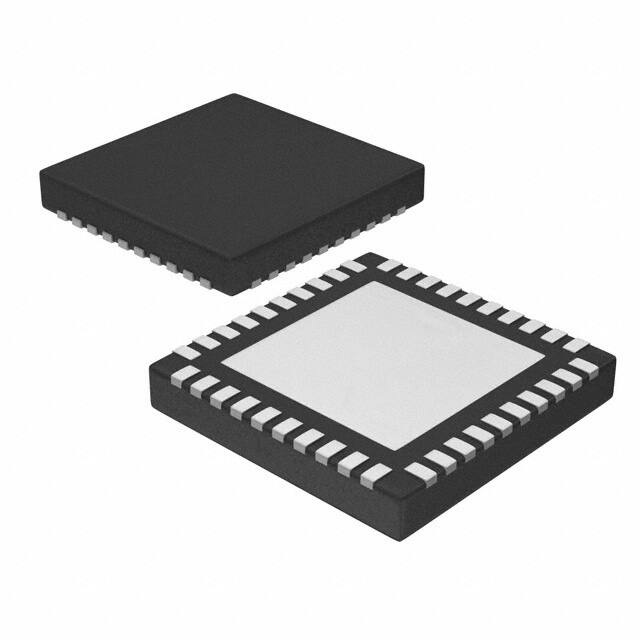


 工商网监
湘ICP备2023018690号
工商网监
湘ICP备2023018690号
