www.ti.com
Table of Contents
User’s Guide
TPS51218 Buck Controller Evaluation Module User's
Guide
ABSTRACT
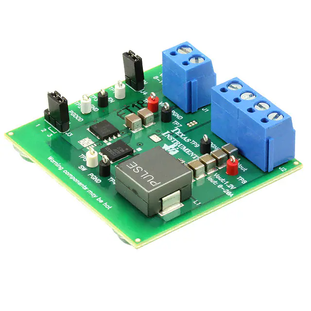
The TPS51218EVM evaluation module (EVM) is used to evaluate the TPS51218, a small-size, single buck
controller with adaptive on-time D-CAP™ mode, providing a fixed 1.2-V output at up to 20 A from a 12-V input
bus.
Table of Contents
1 Description.............................................................................................................................................................................. 2
1.1 Typical Applications............................................................................................................................................................2
1.2 Features............................................................................................................................................................................. 2
2 Electrical Performance Specifications................................................................................................................................. 2
3 Schematic................................................................................................................................................................................3
4 Test Setup................................................................................................................................................................................4
4.1 Test Equipment.................................................................................................................................................................. 4
4.2 Recommended Test Setup.................................................................................................................................................5
5 Test Procedure........................................................................................................................................................................ 7
5.1 Line/Load Regulation and Efficiency Measurement Procedure......................................................................................... 7
5.2 List of Test Points............................................................................................................................................................... 7
5.3 Equipment Shutdown......................................................................................................................................................... 7
6 Performance Data and Typical Characteristic Curves........................................................................................................ 8
6.1 Efficiency............................................................................................................................................................................8
6.2 Load Regulation................................................................................................................................................................. 8
6.3 Transient Response........................................................................................................................................................... 9
6.4 Output Ripple................................................................................................................................................................... 10
6.5 Switch Node Voltage........................................................................................................................................................ 10
6.6 Turn-On Waveform........................................................................................................................................................... 11
6.7 Turn-Off Waveform........................................................................................................................................................... 11
6.8 Output 1.1-V Prebias Turn-On......................................................................................................................................... 12
7 EVM Assembly Drawing and PCB Layout.......................................................................................................................... 13
8 Bill of Materials..................................................................................................................................................................... 16
9 Revision History................................................................................................................................................................... 16
Trademarks
D-CAP™ are trademarks of Texas Instruments.
All trademarks are the property of their respective owners.
SLVU346A – JANUARY 2010 – REVISED FEBRUARY 2022
TPS51218 Buck Controller Evaluation Module User's Guide
Submit Document Feedback
Copyright © 2022 Texas Instruments Incorporated
1
�Description
www.ti.com
1 Description
The TPS51218EVM is designed to use a regulated 12-V bus to produce a regulated 1.2-V output at up to 20 A of
load current. The TPS51218EVM is designed to demonstrate the TPS51218 in a typical, low-voltage application
while providing a number of test points to evaluate the performance of the TPS51218.
1.1 Typical Applications
•
•
•
•
•
•
•
•
High-current system converters for server and desktop power
Switchers and routers
Embedded computers
In-vehicle infotainment PCs
POS terminals
Point-of-load modules
Graphics cards
Industrial control/factory automation PCs
1.2 Features
The TPS51218EVM features:
•
•
•
•
•
•
20-ADC steady-state current
Support prebias output voltage start-up
380-kHz switching frequency
J4 for enable function
J3 for auto-skip and forced CCM selection
Convenient test points for probing critical waveforms
2 Electrical Performance Specifications
Table 2-1. TPS51218EVM Electrical Performance Specifications
Parameter
Test Conditions
Min
Typ
Max
8
12
14
Units
INPUT CHARACTERISTICS
Voltage range
VIN
Maximum input current
VIN = 8 V, IO = 20 A
No load input current
VDC = 14 V, IO = 0 A
3.55
50
V
A
mA
OUTPUT CHARACTERISTICS
Output voltage, VOUT
Output voltage regulation
Output voltage ripple
1.2
Line regulation (VDC = 10 V–14 V)
1.0%
Load regulation (VDC = 12 V, IO = 0 A–20 A)
1.0%
VIN = 12 V, IO = 20 A
Output load current
0
Output overcurrent
V
40
mVpp
20
A
30
A
380
kHz
SYSTEMS CHARACTERISTICS
Switching frequency
Peak efficiency
VIN = 12 V, 1.2 V/10 A
90.32%
Full-load efficiency
VIN = 12 V, 1.2 V/20 A
88.64%
Operating temperature
2
25
TPS51218 Buck Controller Evaluation Module User's Guide
°C
SLVU346A – JANUARY 2010 – REVISED FEBRUARY 2022
Submit Document Feedback
Copyright © 2022 Texas Instruments Incorporated
�PWM
Mode
ENABLE
EN
PGND
PGOOD
GND
Not used
PWM Mode selection :
1. Jumper on pin 2 and pin 3 of J3: Setting auto - skip mode ( Default setting )
2. Jumper on pin 1 and pin 2 of J3: Setting forced CCM mode .
Enable Notes :
1. Jumper shorted on J 4 to disable the controller .( Default setting )
2. No jumper on J 4 to enable the controller .
PGND
PGND
SW
PGND
Vin
PGND
Vout
www.ti.com
Schematic
3 Schematic
Figure 3-1. TPS51218EVM Schematic
SLVU346A – JANUARY 2010 – REVISED FEBRUARY 2022
TPS51218 Buck Controller Evaluation Module User's Guide
Submit Document Feedback
Copyright © 2022 Texas Instruments Incorporated
3
�Test Setup
www.ti.com
4 Test Setup
4.1 Test Equipment
Voltage Source: The input voltage source, VIN, must be a 0-V to 14-V variable DC source capable of supplying
10 ADC. Connect VIN to J1 as shown in Figure 4-2.
Multimeters: A 0-V to 15-V voltmeter must be used to measure VIN at TP6 (VIN) and TP7 (PGND) and a 0-V
to 5-V voltmeter for VOUT measurement at TP8 (VOUT) and TP9 (PGND). A 0-A to 10-A current meter (A1) as
shown in Figure 4-2 is used for input current measurements.
Output Load: The output load must be an electronic constant resistance mode load capable of 0 ADC to 30 ADC
at 1.2 V.
Oscilloscope: A digital or analog oscilloscope can be used to measure the output ripple. The oscilloscope must
be set for the following:
•
•
•
•
•
1-MΩ impedance
20-MHz bandwidth
AC coupling
2-µs/division horizontal resolution
50-mV/division vertical resolution
Test points TP8 and TP9 can be used to measure the output ripple voltage by placing the oscilloscope probe tip
through TP8 and holding the ground barrel TP9 as shown in Figure 4-1. Using a leaded ground connection can
induce additional noise due to the large ground loop.
Metal Ground Barrel
Probe Tip
TP8
TP9
Figure 4-1. Tip and Barrel Measurement for VOUT Ripple
Fan: Some of the components in this EVM can get hot, approaching temperatures up to 60°C during operation.
A small fan capable of 200 to 400 LFM is recommended to reduce component temperatures while the EVM is
operating. The EVM must not be probed while the fan is not running.
Recommended Wire Gauge: For VIN to J1 (12-V input), the recommended wire size is 1× AWG 14 per input
connection, with the total length of wire less than four feet (2-foot input, 2-foot return). For J2 to LOAD, the
minimum recommended wire size is 2× AWG 14, with the total length of wire less than four feet (2-foot output,
2-foot return).
4
TPS51218 Buck Controller Evaluation Module User's Guide
SLVU346A – JANUARY 2010 – REVISED FEBRUARY 2022
Submit Document Feedback
Copyright © 2022 Texas Instruments Incorporated
�www.ti.com
Test Setup
4.2 Recommended Test Setup
DC
Source
Vin
+
-
+
-
A1
Load
V1
V2
FAN
TEXAS
INSTRUMENTS
Figure 4-2. TPS51218EVM Recommended Test Setup
Figure 4-2 shows the recommended test setup to evaluate the TPS51218EVM. Working at an ESD workstation,
ensure that any wrist straps, bootstraps, or mats are connected referencing the user to earth ground before
power is applied to the EVM.
4.2.1 Configurations
•
•
EN J4 setting
1. No jumper enables the controller.
2. A jumper shorted on J4 disables the controller (default setting).
PWM J3 setting
1. A jumper on pin 2 and pin 3 of J3 set the auto-skip mode (default setting).
2. A jumper on pin 1 and pin 2 of J3 sets a forced CCM mode.
4.2.2 Input Connections
1. Prior to connecting the DC input source VIN, it is advisable to limit the source current from VIN to 10 A
maximum. Ensure that VIN is initially set to 0 V and connected as shown in Figure 4-2.
2. Connect a voltmeter V1 at TP6 (VIN) and TP7 (PGND) to measure the input voltage.
3. Connect a current meter A1 to measure the input current.
4.2.3 Output Connections
1. Connect the load to J2, and set the load to constant resistance mode to sink 0 ADC before VIN is applied.
2. Connect a voltmeter V2 at TP8 (VOUT) and TP9 (PGND) to measure the output voltage.
SLVU346A – JANUARY 2010 – REVISED FEBRUARY 2022
TPS51218 Buck Controller Evaluation Module User's Guide
Submit Document Feedback
Copyright © 2022 Texas Instruments Incorporated
5
�Test Setup
www.ti.com
4.2.4 Other Connections
Place a fan as shown in Figure 4-2 and turn it on, making sure that air is flowing across the EVM.
6
TPS51218 Buck Controller Evaluation Module User's Guide
SLVU346A – JANUARY 2010 – REVISED FEBRUARY 2022
Submit Document Feedback
Copyright © 2022 Texas Instruments Incorporated
�www.ti.com
Test Procedure
5 Test Procedure
5.1 Line/Load Regulation and Efficiency Measurement Procedure
1.
2.
3.
4.
5.
6.
7.
8.
9.
10.
Ensure that the load is set to constant resistance mode and to sink 0 ADC.
Ensure that the jumper provided in the EVM to short J4 is on before VIN is applied.
Ensure that the jumper provided in the EVM to short pin 2 and pin 3 of J3 is on before VIN is applied.
Increase VIN from 0 V to 12 V. Use V1 to measure the input voltage.
Remove the jumper on J4 to enable the controller.
Vary the load from 0 ADC to 20 ADC. VOUT must remain in load regulation.
Vary VIN from 8 V to 14 V. VOUT must remain in line regulation.
Put the jumper on J4 to disable the controller.
Decrease the load to 0 A.
Decrease VIN to 0 V.
5.2 List of Test Points
Table 5-1. The Functions of Each Test Points
Test Points
Name
Description
TP1
EN
Enable
TP2
PGOOD
Power Good
TP3
GND
GND
TP4
PGND
PGND
TP5
SW
Switching node
TP6
Vin
Vin
TP7
PGND
GND for Vin
TP8
Vout
Vout
TP9
PGND
PGND
5.3 Equipment Shutdown
1. Shut down the load.
2. Shut down VIN.
3. Shut down the fan.
SLVU346A – JANUARY 2010 – REVISED FEBRUARY 2022
TPS51218 Buck Controller Evaluation Module User's Guide
Submit Document Feedback
Copyright © 2022 Texas Instruments Incorporated
7
�Performance Data and Typical Characteristic Curves
www.ti.com
6 Performance Data and Typical Characteristic Curves
Figure 6-1 through Figure 6-9 present typical performance curves for the TPS51218EVM.
6.1 Efficiency
100
8 Vin auto skip
90
12 Vin auto skip
80 14 Vin auto skip
Efficiency - %
70
8 Vin forced CCM
60
50
12 Vin forced CCM
40
14 Vin forced CCM
30
20
10
0
0.001
0.01
0.1
1
IO - Output Current - A
10
100
Figure 6-1. TPS51218EVM Efficiency
6.2 Load Regulation
1.27
1.26
VO - Output Volatge - V
14 Vin forced CCM
1.25
12 Vin forced CCM
8 Vin forced CCM
1.24
1.23
1.22
14 Vin auto skip
12 Vin auto skip
8 Vin auto skip
1.21
1.2
0.001
0.01
0.1
1
IO - Output Current - A
10
100
Figure 6-2. TPS51218 Load Regulation
8
TPS51218 Buck Controller Evaluation Module User's Guide
SLVU346A – JANUARY 2010 – REVISED FEBRUARY 2022
Submit Document Feedback
Copyright © 2022 Texas Instruments Incorporated
�www.ti.com
Performance Data and Typical Characteristic Curves
6.3 Transient Response
TPS51218EVM Transient Response
12 Vin, 1.2 V/5A-15A Auto skip
CH1: 1.2 Voutput
CH2: Output Current
t - Time - 200 ms/div
Figure 6-3. TPS51218EVM Load Transient
TPS51218EVM Transient Response
12 Vin, 1.2 V/0A-10A Auto skip
CH1: 1.2 Voutput
CH2: Output Current
t - Time - 200 ms/div
Figure 6-4. TPS51218EVM Load Transient
SLVU346A – JANUARY 2010 – REVISED FEBRUARY 2022
TPS51218 Buck Controller Evaluation Module User's Guide
Submit Document Feedback
Copyright © 2022 Texas Instruments Incorporated
9
�Performance Data and Typical Characteristic Curves
www.ti.com
6.4 Output Ripple
TPS51218EVM Output Ripple
12 Vin, 1.2 V/20A Forced PWM
CH1: 1.2 Vout Ripple
t - Time - 2 ms/div
Figure 6-5. Output Ripple
6.5 Switch Node Voltage
TPS51218EVM Switching Node
12 Vin, 1.2 V/20A Forced PWM
CH1: SW
t - Time - 80 ns/div
Figure 6-6. Switching Node Waveform
10
TPS51218 Buck Controller Evaluation Module User's Guide
SLVU346A – JANUARY 2010 – REVISED FEBRUARY 2022
Submit Document Feedback
Copyright © 2022 Texas Instruments Incorporated
�www.ti.com
Performance Data and Typical Characteristic Curves
6.6 Turn-On Waveform
TPS51218EVM Enable Start up
12 Vin, 1.2 V/20A Auto skip
CH1: 12 Vin
CH2: Enable
CH3: 1.2 Vout
CH4: PGOOD
t - Time - 1 ms/div
Figure 6-7. Enable Turn-On Waveform
6.7 Turn-Off Waveform
TPS51218EVM Enable Shut down
12 Vin, 1.2 V/20A Auto skip
CH1: 12 Vin
CH2: Enable
CH3: 1.2 Vout
CH4: PDOOD
t - Time - 1 ms/div
Figure 6-8. Enable Turn-Off Waveform
SLVU346A – JANUARY 2010 – REVISED FEBRUARY 2022
TPS51218 Buck Controller Evaluation Module User's Guide
Submit Document Feedback
Copyright © 2022 Texas Instruments Incorporated
11
�Performance Data and Typical Characteristic Curves
www.ti.com
6.8 Output 1.1-V Prebias Turn-On
TPS51218EVM Enable Pre-bias start up
1.1 V output pre-bias
12 Vin, 1.2 V/0A forced PWM
CH1: 1.2 Vin
CH2: Enable
CH3: 1.2 Vout
CH4: PGOOD
t - Time - 1 ms/div
Figure 6-9. Output 1.1-V Prebias TurnOn
12
TPS51218 Buck Controller Evaluation Module User's Guide
SLVU346A – JANUARY 2010 – REVISED FEBRUARY 2022
Submit Document Feedback
Copyright © 2022 Texas Instruments Incorporated
�www.ti.com
EVM Assembly Drawing and PCB Layout
7 EVM Assembly Drawing and PCB Layout
Figure 7-1 through Figure 7-6 show the design of the TPS51218EVM printed-circuit board. The EVM has been
designed using a four-layer, 2-oz copper circuit board.
TEXAS
INSTRUMENTS
Figure 7-1. TPS51218EVM Top Layer Assembly Drawing, Top View
Figure 7-2. TPS51218EVM Bottom Assembly Drawing, Bottom View
SLVU346A – JANUARY 2010 – REVISED FEBRUARY 2022
TPS51218 Buck Controller Evaluation Module User's Guide
Submit Document Feedback
Copyright © 2022 Texas Instruments Incorporated
13
�EVM Assembly Drawing and PCB Layout
www.ti.com
Figure 7-3. TPS51218EVM Top Copper, Top View
Figure 7-4. TPS51218EVM Internal Layer 1
14
TPS51218 Buck Controller Evaluation Module User's Guide
SLVU346A – JANUARY 2010 – REVISED FEBRUARY 2022
Submit Document Feedback
Copyright © 2022 Texas Instruments Incorporated
�www.ti.com
EVM Assembly Drawing and PCB Layout
Figure 7-5. TPS51218EVM Internal Layer 2
Figure 7-6. TPS51218EVM Bottom Layer
SLVU346A – JANUARY 2010 – REVISED FEBRUARY 2022
TPS51218 Buck Controller Evaluation Module User's Guide
Submit Document Feedback
Copyright © 2022 Texas Instruments Incorporated
15
�Bill of Materials
www.ti.com
8 Bill of Materials
The EVM components are shown in Table 8-1 according to the schematic shown in Figure 3-1.
Table 8-1. Bill of Materials
QTY
REFDES
Description
MFR
Part Number
2
C9, C12
Capacitor, Ceramic, 22 µF, 16 V, X5R, 10%, 1210
Murata
GRM32ER61C226KE20L
1
C3
Capacitor, Ceramic, 1 µF, 16 V, X7R, 10%, 0603
STD
STD
2
C1, C16
Capacitor, Ceramic, 0.022 µF, 16 V, X7R, 10%, 0603
STD
STD
1
C8
Capacitor, Ceramic, 3300 pF, 25 V, X7R, 10%, 0603
STD
STD
3
C4, C5, C6
Capacitor, Ceramic, 10 µF, 16 V, X5R, 10%, 0805
STD
STD
2
C7, C17
Capacitor, Ceramic, 0.1 µF, 25 V, X7R, 10%, 0603
STD
STD
5
C10, C11, C13,
C14, C15
Capacitor, Ceramic, 100 µF, 6.3 V, X5R, 20%, 1210
Murata
GRM32ER60J107ME20L
1
L1
Inductor, SMT, 0.44 µH, 30 A, 0.0032 Ω, 0.530" × 0.510"
Pulse
PA0513.441NLT
E&E Magnetic
831-02990F
1
Q1
MOSFET, Nchan, 25 V, 21 A, 4.1 mΩ, QFN5X6mm
TI (Ciclon)
CSD16404Q5A
2
Q2, Q4
MOSFET, Nchan, 25 V, 31 A, 2.1 mΩ, QFN5X6mm
TI(Ciclon)
CSD16321Q5
3
R1, R11, R13
Resistor, Chip, 10 k, 1/16W, 1%, 0603
STD
STD
1
R10
Resistor, Chip, 7.15 k, 1/16W, 1%, 0603
STD
STD
1
R3
Resistor, Chip, 19.6 k, 1/16W, 1%, 0603
STD
STD
2
R2, R12
Resistor, Chip, 100 k, 1/16W, 1%, 0603
STD
STD
2
R6, R7
Resistor, Chip, 0, 1/16W, 1%, 0603
STD
STD
1
R4
Resistor, Chip, 3.01, 1/16W, 1%, 0603
1
R5
Resistor, Chip, 2.37, 1/16W, 1%, 0603
STD
STD
2
R8, R9
Resistor, Chip, 1, 1/16W, 5%, 0805
STD
STD
1
U2
IC, Integrated LDO with switch-over circuit, DGS10
TI
TPS51103DRC
1
U1
IC, Synchronous step-down controller, DSC10
TI
TPS51218DSC
9 Revision History
NOTE: Page numbers for previous revisions may differ from page numbers in the current version.
Changes from Revision * (January 2010) to Revision A (February 2022)
Page
• Updated the numbering format for tables, figures, and cross-references throughout the document. ................2
• Updated the user's guide title............................................................................................................................. 2
16
TPS51218 Buck Controller Evaluation Module User's Guide
SLVU346A – JANUARY 2010 – REVISED FEBRUARY 2022
Submit Document Feedback
Copyright © 2022 Texas Instruments Incorporated
�IMPORTANT NOTICE AND DISCLAIMER
TI PROVIDES TECHNICAL AND RELIABILITY DATA (INCLUDING DATA SHEETS), DESIGN RESOURCES (INCLUDING REFERENCE
DESIGNS), APPLICATION OR OTHER DESIGN ADVICE, WEB TOOLS, SAFETY INFORMATION, AND OTHER RESOURCES “AS IS”
AND WITH ALL FAULTS, AND DISCLAIMS ALL WARRANTIES, EXPRESS AND IMPLIED, INCLUDING WITHOUT LIMITATION ANY
IMPLIED WARRANTIES OF MERCHANTABILITY, FITNESS FOR A PARTICULAR PURPOSE OR NON-INFRINGEMENT OF THIRD
PARTY INTELLECTUAL PROPERTY RIGHTS.
These resources are intended for skilled developers designing with TI products. You are solely responsible for (1) selecting the appropriate
TI products for your application, (2) designing, validating and testing your application, and (3) ensuring your application meets applicable
standards, and any other safety, security, regulatory or other requirements.
These resources are subject to change without notice. TI grants you permission to use these resources only for development of an
application that uses the TI products described in the resource. Other reproduction and display of these resources is prohibited. No license
is granted to any other TI intellectual property right or to any third party intellectual property right. TI disclaims responsibility for, and you
will fully indemnify TI and its representatives against, any claims, damages, costs, losses, and liabilities arising out of your use of these
resources.
TI’s products are provided subject to TI’s Terms of Sale or other applicable terms available either on ti.com or provided in conjunction with
such TI products. TI’s provision of these resources does not expand or otherwise alter TI’s applicable warranties or warranty disclaimers for
TI products.
TI objects to and rejects any additional or different terms you may have proposed. IMPORTANT NOTICE
Mailing Address: Texas Instruments, Post Office Box 655303, Dallas, Texas 75265
Copyright © 2022, Texas Instruments Incorporated
�


 工商网监
湘ICP备2023018690号
工商网监
湘ICP备2023018690号
