TPS5140
FOUR-CHANNEL DC/DC CONTROLLER FOR NOTEBOOK PC POWER
SLVS305A – DECEMBER 2000 – REVISED JANUARY 2001
D
D
D
D
D
D
D
D
description
LL2
OUT2_u
INV1
NC
NC
LH1
OUT1_u
LL1
NC
OUT1_d
OUTGND1
TRIP1
V CC _SENSE12
TRIP2
OUTGND2
OUT2_d
D
PAG PACKAGE
(TOP VIEW)
64 63 62 61 60 59 58 57 56 55 54 53 52 51 50 49
1
48
2
47
3
46
4
45
5
44
6
43
7
42
8
41
9
40
10
39
11
38
12
37
13
36
14
35
15
34
16
33
17 18 19 20 21 22 23 24 25 26 27 28 29 30 31 32
SCP
D
D
Three Independent Step-Down DC/DC
Controllers and One 12-V Boost DC/DC
Converter
4.5 V – 28 V Input Voltage Range
Step-Down Controller Output Voltages
Adjustable Down to 1.2 V
Synchronous-Buck Operation for High
FB1
Efficiency
SOFTSTART1
PWM Mode Control
NC
INV2
Auto PWM/SKIP Mode for High
FB2
Efficiency Under All Load Conditions
SOFTSTART2
PWM_SEL
High Speed Error Amplifier
Ct
Separate Standby Control and Over
GND
Current Protection for Each Channel
REF
STBY_VREF3.3
Over Voltage and Under Voltage
STBY_VREF5
Protection
STBY1
STBY2
Programmable Short Circuit Protection
STBY12V
Power Good With Programmable Delay
STBY3
Time
5 V and 3.3 V Linear Regulators
LH2
NC
VCC
NC
VREF3.3
VREF5
REG5V_IN
NC
GND_UP
LL_UP
IN_12V
OUT_12V
NC
VCC_SENSE3
TRIP3
NC
PGOUT
PG–DELAY
NC
EXT_PG
OFTSTART_12V
PHASE_12V
SOFTSTART3
FB3
INV3
NC
LH3
OUT3_u
LL3
OUT3_d
OUTGND3
D
The TPS5140 is a dc/dc controller that incorporates three synchronous-buck controllers and one
nonsynchronous 12-V boost converter on one chip to power the voltage rails needed by notebook peripheral
components. On-chip high-side and low-side synchronous rectifier drivers are integrated to drive less expensive
N-channel power MOSFETs. The nonsynchronous boost converter includes the N channel power MOSFET and
supports 120 mA for the PCMCIA power supply. The outputs are controlled independently and two of the
synchronous-buck controllers operate 180 degrees out of phase, with the third lowering the input current ripple
and allowing a smaller input capacitance to reduce power supply cost. For higher efficiency under all load
conditions, the TPS5140 automatically adjusts each channel from the PWM mode to the skip mode
independently. The skip mode enables a lower operating frequency and shortens the pulse width to the low side
MOSFETs, thereby increasing the efficiency under light load conditions. To further extend battery life, the
TPS5140 features dead-time control and very low quiescent current. Resistorless current protection and the
fixed high-side driver voltage simplify the system design and reduce the external parts count.
Please be aware that an important notice concerning availability, standard warranty, and use in critical applications of
Texas Instruments semiconductor products and disclaimers thereto appears at the end of this data sheet.
Copyright 2001, Texas Instruments Incorporated
PRODUCTION DATA information is current as of publication date.
Products conform to specifications per the terms of Texas Instruments
standard warranty. Production processing does not necessarily include
testing of all parameters.
POST OFFICE BOX 655303
• DALLAS, TEXAS 75265
1
�TPS5140
FOUR-CHANNEL DC/DC CONTROLLER FOR NOTEBOOK PC POWER
SLVS305A – DECEMBER 2000 – REVISED JANUARY 2001
typical design schematic
VO1
C23
R14
C16
R10
R11
L1
VI
Q1
Q2
C22
R12
R1
R1
R9
C17
Q3
C26
C27
C1
C15
R8
GND
C18
D1
L2
R3
C2
SOFTSTART1
INV2
FB2
C3
LL2
IN_12V
OUTGND3
LL3
L4
LL_UP
OUT3_d
LH3
C6
C21
OUT3_u
SCP
VO5
C13
C12
D4
VO4
OUT_12V
VCC_SENSE3
INV3
REF
SOFTSTART3
FB3
C5
LH2
VCC
TPS5140IPAG
CT
GND
D2
VREF3.3
VREF5
GND_UP
U1
SOFTSTART2
C4
OUT2_u
INV1
LH1
OUT1_u
FB1
LL1
OUT1_d
OUTGND1
TRIP1
VCC_SENSE12
TRIP2
OUTGND2
OUT2_d
C14
C19
R2
VO2
R17 Q4
R18
R7
TRIP3
C25
Q5
C11
R4
C10
C9
C8
VO3
R16
L3
Q6
D3
R6
R5
R15
C20
C24
AVAILABLE OPTIONS
TA
– 20°C to 85°C
2
PACKAGE
PAG
EVM
TQFP64 (PAG)
POST OFFICE BOX 655303
• DALLAS, TEXAS 75265
�TPS5140
FOUR-CHANNEL DC/DC CONTROLLER FOR NOTEBOOK PC POWER
SLVS305A – DECEMBER 2000 – REVISED JANUARY 2001
functional block diagram—whole block
SBRC Ch1
SBRC Ch2
SBRC Ch3
Phase
Inverter
Oscillator
Timer
12-V Boost
Converter
Ch4
OUT_12 V
REG5V_IN
5-V Switch
3.3-V Series
Regulator
VREF5
VCC
VREF3.3
5-V Series
Regulator
50 mA
Vref 1.185 V
POST OFFICE BOX 655303
• DALLAS, TEXAS 75265
3
�TPS5140
FOUR-CHANNEL DC/DC CONTROLLER FOR NOTEBOOK PC POWER
SLVS305A – DECEMBER 2000 – REVISED JANUARY 2001
functional block diagram—SMPS block
Skip Comparator
+
Error Amplifier
PWM
Comparator
OUT_u
INV1
MOSFET
Driver
+
OUT_d
Phase Inverter
Ct
Oscillator
OVP (1.185 V + 12 %)
OVP (1.185 V – 18 %)
PG Comparator
Timer
Current
Limit
SCP
4
SOFTSTART
Softstart
STBY
Standby
POST OFFICE BOX 655303
• DALLAS, TEXAS 75265
TRIP
�TPS5140
FOUR-CHANNEL DC/DC CONTROLLER FOR NOTEBOOK PC POWER
SLVS305A – DECEMBER 2000 – REVISED JANUARY 2001
functional block diagram—boost 12-V block
OUT_12 V
Error Amplifier
PWM Comparator
_
+
+
+
_
+
Current
Limit
LL_UP
NMOS
OSC
MOS
Driver
GND_UP
Softstart 12 V
SFT_12V
OVP
UVP
IN_12V
Timer
PMOS
SCP
OUT_12V
REG5V_IN
REG5V_IN
OVP
PMOS
VREF5
_
+
+
STBY_12V
POST OFFICE BOX 655303
• DALLAS, TEXAS 75265
5
�TPS5140
FOUR-CHANNEL DC/DC CONTROLLER FOR NOTEBOOK PC POWER
SLVS305A – DECEMBER 2000 – REVISED JANUARY 2001
functional block diagram—power good block
STBY_VREF5
STBY_VREF3.3
3.3-V Series
Regulator
VREF3.3
UVLO
VCC
5-V Series
Regulator
50 mA Max.
REF
Vref
1.185 V
VREF5
_
+
REG5V_IN
+
4.5 V
EXT_PG
PG_DELAY
Timer
OR Logic
PGOUT
(open drain)
6
POST OFFICE BOX 655303
• DALLAS, TEXAS 75265
PG Comp.1
PG Comp.2
PG Comp.3
�TPS5140
FOUR-CHANNEL DC/DC CONTROLLER FOR NOTEBOOK PC POWER
SLVS305A – DECEMBER 2000 – REVISED JANUARY 2001
Terminal Functions
TERMINAL
NAME
NO.
I/O
Ct
8
EXT_PG
21
I
External power good signal input
FB1
1
O
Feedback output of CH1 error amplifier
FB2
5
O
Feedback output of CH2 error amplifier
FB3
25
O
Feedback output of CH3 error amplifier
GND
9
GND_UP
40
INV1
64
I
Inverting input of CH1 error amplifier, skip comparator and OVP1/UVP1, PG comparator
INV2
4
I
Inverting input of CH1 error amplifier, skip comparator and OVP2/UVP2, PG comparator
INV3
26
I
Inverting input of CH1 error amplifier, skip comparator and OVP3/UVP3, PG comparator
IN_12V
38
I
Input of PMOS switch for 12-V boost output. Connecting to cathode of the external Schottky
diode.
LH1
61
I/O
Bootstrap capacitor connection for CH1 high side gate drive
LH2
48
I/O
Bootstrap capacitor connection for CH2 high side gate drive
LH3
28
I/O
Bootstrap capacitor connection for CH3 high side gate drive
LL1
59
I/O
Bootstrap low for CH1 high side gate driving return and output current protection. Connect to
the junction of the high side and low side FETs for floating drive configuration.
LL2
50
I/O
Bootstrap low for CH2 high side gate driving return and output current protection. Connect to
the junction of the high side and low side FETs for floating drive configuration.
LL3
30
I/O
Bootstrap low for CH3 high side gate driving return and output current protection. Connect to
the junction of the high side and low side FETs for floating drive configuration.
LL_UP
39
I/O
Open drain output of internal NMOS switch for 12-V boost converter. Connect between external inductor and the anode of the schottky diode.
NC
I/O
DESCRIPTION
External capacitor from Ct to GND used for adjusting the triangle oscillator.
Control GND
Ground for 12-V boost converter
3,20,27,33,
36,41,45,47
58,62,63
No connect
OUT1_d
57
O
Gate drive output for CH1 low side gate drive
OUT2_d
51
O
Gate drive output for CH2 low side gate drive
OUT3_d
31
O
Gate drive output for CH3 low side gate drive
OUT1_u
60
O
Gate drive output for CH1 high side switching FETs
OUT2_u
49
O
Gate drive output for CH2 high side switching FETs
OUT3_u
29
O
Gate drive output for CH3 high side switching FETs
OUT_12V
37
O
Output of PMOS switch for 12-V boost output. Connect to the output capacitor for 12-V boost
output.
OUTGND1
56
Ground for CH1 FETs drivers. It is connected to one of the current limiting comparator input.
OUTGND2
52
Ground for CH2 FETs drivers. It is connected to one of current limiting comparator input.
OUTGND3
32
PGOUT
18
O
Open drain output for power good signal
PG_DELAY
19
I/O
Programmable delay for power good. Connect to the external capacitor for timer delay.
PHASE_12V
23
I
Phase compensation for the12-V boost converter. Connect to an external capacitor.
But normally it is not connected.
PWM_SEL
7
I
PWM or auto PWM/SKIP modes select
L: PWM fixed
H: auto PWM/SKIP
REF
10
O
1.185 V reference voltage output
Ground for CH3 FETs drivers. It is connected to the one of current limiting comparator input.
POST OFFICE BOX 655303
• DALLAS, TEXAS 75265
7
�TPS5140
FOUR-CHANNEL DC/DC CONTROLLER FOR NOTEBOOK PC POWER
SLVS305A – DECEMBER 2000 – REVISED JANUARY 2001
Terminal Functions(Continued)
TERMINAL
NAME
NO.
I/O
DESCRIPTION
REG5V_IN
42
I
External 5 V input
SCP
17
I/O
Short circuit protection terminal. An external capacitor is connected between SCP and GND to
set the SCP enable time up.
SOFTSTART1
2
I/O
External capacitor from SOFTSTART1 to GND for CH1 soft starts control.
SOFTSTART2
6
I/O
External capacitor from SOFTSTART2 to GND for CH2 soft starts control.
SOFTSTART3
24
I/O
External capacitor from SOFTSTART3 to GND for CH3 soft starts control.
SOFTSTART_12V
22
I/O
External capacitor from SOFTSTART_12V to GND for CH4 (12-V boost converter) soft starts
control.
STBY1
13
I
Stand by control for CH1
STBY2
14
I
Stand by control for CH2
STBY3
16
I
Stand by control for CH3
STBY12V
15
I
Stand by control for 12-V boost converter
STBY_VREF3.3
11
I
Stand by control for 3.3-V linear regulator
STBY_VREF5
12
I
Stand by control for 5-V linear regulator
TRIP1
55
I
External resistor connection for CH1 output current protection control
TRIP2
53
I
External resistor connection for CH2 output current protection control
TRIP3
34
I
External resistor connection for CH3 output current protection control
VCC
VCC_SENSE12
46
54
I
Supply voltage input and input voltage terminal for CH1/2 output current sense
VCC_SENSE3
VREF3.3
35
I
Supply voltage input and input voltage terminal for CH3 output current sense
44
O
3.3-V linear regulator output
VREF5
43
O
5-V linear regulator output
Supply voltage input
detailed description
REF (1.185 V)
The reference voltage is used for setting the output voltage and voltage protection. This reference voltage is
dropped down from the 5-V regulator. The tolerance is 1.5 % over the entire temperature range.
CH1, 2, 3 (synchronous buck controller)
The TPS5140 includes three synchronous buck controllers. CH2 and CH3 (5 V and 2.5 V) are operated in phase,
but CH1 (3.3 V) is operated 180° out of phase from CH2 and CH3, but at the same frequency. All channels have
separate standby and softstart control.
12-V boost converter
OUT_12V is a 12-V boost converter output . It can isolate VI (5 V) and VO fully.
5-V regulator
An internal linear voltage regulator is used for the high-side driver bootstrap voltage and as the source of Vref.
When the 5-V regulator is disconnected from the MOSFET drivers, it is used only for the source of Vref. Since
the input voltage is from 4.5 V to 28 V, this feature offers a fixed bootstrap voltage to simplify the drive design.
The 5-V regulator is also used for powering the low side driver. The 5-V regulator is active if STBY_VREF5 is
high and has a tolerance of 4%.
8
POST OFFICE BOX 655303
• DALLAS, TEXAS 75265
�TPS5140
FOUR-CHANNEL DC/DC CONTROLLER FOR NOTEBOOK PC POWER
SLVS305A – DECEMBER 2000 – REVISED JANUARY 2001
detailed description (continued)
3.3-V regulator
TPS5140 has a 3.3-V linear regulator. The output is made from the internal 5 V regulator or external 5 V from
REG5V_IN. The 3.3-V regulator has an output current limit. The maximum output current is 30 mA.
5-V switch
If the internal 5-V switch senses a 5-V input from the REG5V_IN terminal, the internal 5-V linear regulator will
be disconnected from the MOSFET drivers. The external 5 V will be used for both the low-side driver and the
high-side bootstrap, thus increasing the efficiency.
auto PWM/SKIP
The PWM_SEL terminal selects either the auto PWM/SKIP or fixed PWM mode. If this terminal is lower than
0.5 V, the outputs operate in the fixed PWM mode. If 2.5 V (minimum) is applied, the outputs operate in auto
PWM/SKIP mode. In the auto PWM/SKIP mode, the operation changes from the PWM mode to the SKIP mode
automatically under light load conditions. Avoid using a MOSFET with very low rDS(on) if the auto SKIP function
is implemented.
error amp
All three synchronous buck channels have their own error amplifier to regulate the output. The error amplifier
is used in the PWM mode for high output current conditions (> 0.2 A). Voltage mode control is implemented.
skip comparator
In skip mode, all three synchronous buck channels have their own hysteresis comparator to regulate the output
voltages. The hysteresis voltage is set internally and typically at 8.5 mV. The delay from the comparator input
to the driver output is typically 1.2 µs.
low-side driver
The low-side driver is designed to drive low-rDS(on) n-channel MOSFETs. The maximum drive voltage is 5 V from
VREF5. Ch1, 2, and 3 MOSFET driver capability is 1.5 A, source and sink.
high-side driver
The high-side driver is designed to drive low-rDS(on) n-channel MOSFETs. CH1 and CH2 MOSFET drivers have
1.2 A capability, source and sink. When configured as a floating driver, the bias voltage to the driver is developed
from VREF5, limiting the maximum drive voltage between OUT_u and LL to 5 V. The maximum voltage that can
be applied between LHx and OUTGND is 33 V.
dead time
Dead time prevents shoot-through current from flowing through the main power MOSFETs during switching
transitions by actively controlling the turnon time of the MOSFETs drivers.
current protection
Current protection is achieved by sensing the drain-to-source voltage drop of the low-side power MOSFET
during the low-side MOSFET’s on time at OUTGND and LL. An external resistor between VCC_ SENSE and
TRIP terminal in series with the internal current source adjusts the current limit. When the voltage drop during
the low-side MOSFET on-time is high enough, the current comparator triggers the current protection and the
MOSFET drivers are turned off. After a programmable time delay, the SCP circuit latches off all MOSFET
drivers. The internal current source tolerance is ±10%. CH2 monitors both high-side and low-side MOSFET
voltage drops.
POST OFFICE BOX 655303
• DALLAS, TEXAS 75265
9
�TPS5140
FOUR-CHANNEL DC/DC CONTROLLER FOR NOTEBOOK PC POWER
SLVS305A – DECEMBER 2000 – REVISED JANUARY 2001
detailed description (continued)
OVP
For over voltage protection, the TPS5140 monitors INV terminal voltage. When the INV voltage becomes higher
than 1.185 V (+12%), the OVP comparator output becomes high and the SCP timer starts to charge the SCP
capacitor. After a programmable time delay, the SCP circuit forces CH1, 2, 3 high-side MOSFET drivers to latch
off and the low-side MOSFET drivers to latch on.
UVP
For under voltage protection, the TPS5140 monitors INV terminal voltage. When the INV voltage becomes lower
than 1.185 V (–18 %), the UVP comparator output becomes high and the SCP timer starts to charge the SCP
capacitor. Also, when the current comparator of CH1, 2, 3 triggers the OCP, the UVP comparator detects the
under voltage output and the SCP capacitor starts to charge. After the programmable time delay, the SCP circuit
forces the CH1, 2, 3 MOSFET drivers to latch off.
SCP
When an OVP or UVP comparator output becomes high, the SCP circuit starts to charge the SCP capacitor.
The charging source current value is different between OVP alert and UVP alert.
SCP source current (OVP) = SCP source current (UVP) × 5
The threshold voltage of SCP comparator is 1.185 V.
power good
The power good output reports the output fail condition. PG comparators monitor an under voltage or over
voltage of CH1, 2, 3, with a threshold of –7 % and 7 %. TPS5140 has an EXT_PG terminal, which can be used
for the input of an external PG signal. Delay time is programmable by charging an external capacitor on the
PG_DELAY terminal.
SOFTSTART1, 2, 3
Separate soft start terminals make it possible to customize the start-up time of each output. The voltage on the
charging softstart capacitor gradually raises, limiting the surge current and voltage. A soft start is initiated when
the STBY terminals are switched.
STBY1, 2, 3, 12V
CH1, 2, 3 and 12V can be switched into standby mode separately by grounding the STBY terminal.
STBY_VREF3.3, 5V
STBY_VREF3.3 shuts down the 3.3-V regulator by grounding the STBY_VREF3.3 terminal. When
STBY_VREF5 is high, only the 5-V regulator is operating.
UVLO
When the input voltage exceeds 4 V, the IC is turned on and is ready to function. When the input voltage is lower
than the turn on value, the IC is turned off. The typical hysteresis voltage is 40 mV.
phase inverter
The phase inverter controls the phase of CH1 and CH2, 3. CH2, 3 operate in the same phase as OSC. CH1
operates 180° out of phase from OSC. Out-of-phase operation enables a smaller input capacitor.
OVP (12-V boost converter)
The TPS5140 monitors over voltage of the12-V boost converter. When an output over voltage is detected, the
timer starts to charge an external capacitor that is connected to the SCP terminal. After a programmable time
delay, the SCP circuit forces all (CH1, 2, 3 and 12 V) MOSFET drivers to latch-off.
10
POST OFFICE BOX 655303
• DALLAS, TEXAS 75265
�TPS5140
FOUR-CHANNEL DC/DC CONTROLLER FOR NOTEBOOK PC POWER
SLVS305A – DECEMBER 2000 – REVISED JANUARY 2001
detailed description (continued)
UVP (12-V boost converter)
TPS5140 monitors output under voltage of the 12-V boost converter. When an output under voltage is detected,
the timer starts to charge an external capacitor that is connected to the SCP terminal. After a programmable
time delay, the SCP circuit forces all (CH1, 2, 3, and 12 V) MOSFETs drivers to latch off.
SOFTSTART_12V
An internal capacitor exists for 12-V soft start. If the soft start time needs to be extended, an external capacitor
should be connected to this terminal. The12-V boost converter must start when REG5V_IN terminal is over
4.5 V.
current limit of 12-V boost converter
The 12-V boost current limit monitors the current flowing through the internal MOSFET. When the voltage drop
across the internal N-channel MOSFET is high enough during its on time, the current limit circuit forces the
internal N-channel MOSFET to turn off.
PHASE_12V
The 12-V boost converter does not typically require phase compensation. If there is reason to change the phase,
the 12-V boost converter can be phase compensated by inserting external resistors and capacitors to GND.
Otherwise, the PHASE_12V terminal should be left open.
logic charts
Table 1. Logic Chart1
STBY1
STBY2
STBY3
CH1
CH2
CH3
PGOUT
L
L
L
Disable
Disable
Disable
L
L
H
Disable
Disable
Enable
L
H
L
Disable
Enable
Disable
N/A
Active†
Active†
L
H
H
Disable
Enable
Enable
H
L
L
Enable
Disable
Disable
H
L
H
Enable
Disable
Enable
H
H
L
Enable
Enable
Disable
Active†
Active†
H
H
H
Enable Enable
† During softstart, PGOUT is active low.
Enable
Active†
Active†
Active†
Table 2. Logic Chart2
STBY_VREF5
STBY_VREF3.3
VREF5‡
VREF3.3
L
L
N/A
Disable
H
L
Enable
Disable
L
H
Enable
Enable
H
H
Enable
Enable
‡ To disable VREF5, all STBY1, 2, 3, STBY_VREF3.3 and
STBY_VREF5 must be L.
Table 3. Logic Chart3
STBY12V
REG5V_IN
12 VOUT
L
L
Disable
L
H
Disable
H
L
Disable
H
H
Enable
POST OFFICE BOX 655303
• DALLAS, TEXAS 75265
11
�TPS5140
FOUR-CHANNEL DC/DC CONTROLLER FOR NOTEBOOK PC POWER
SLVS305A – DECEMBER 2000 – REVISED JANUARY 2001
PGOUT timing chart
td1
td2
H
T(SS)
PGOUT
L
H
PG_DELAY
L
H
STBY1
L
H
STBY2
INV1
L
1.185 V
V(TH)
INV2
0V
1.185 V
V(TH)
0V
12
POST OFFICE BOX 655303
• DALLAS, TEXAS 75265
�TPS5140
FOUR-CHANNEL DC/DC CONTROLLER FOR NOTEBOOK PC POWER
SLVS305A – DECEMBER 2000 – REVISED JANUARY 2001
absolute maximum ratings over operating free-air temperature (unless otherwise noted)†
Supply voltage, VCC (see Note 1) . . . . . . . . . . . . . . . . . . . . . . . . . . . . . . . . . . . . . . . . . . . . . . . . . . . –0.3 V to 30 V
Input voltage; INV1/2/3, CT, PWM_SEL, REG5V_IN, SOFTSTART1/2/3, SOFTSTART_12V . –0.3 V to 7 V
SCP, PG_DELAY, PHASE_12V, OUT1/2/3_d, VREF3.3/5, FB1/2/3 . . . . . . . . . . . –0.3 V to 7 V
PGOUT, EXT_PG . . . . . . . . . . . . . . . . . . . . . . . . . . . . . . . . . . . . . . . . . . . . . . . . . . . . . –0.3 V to 7 V
STBY1/2/3/12V, STBY_VREF3.3/5, TRIP1/2/3 . . . . . . . . . . . . . . . . . . . . . . . . . . . –0.3 V to 30 V
VCC_SENSE12/3, LL1/2/3 . . . . . . . . . . . . . . . . . . . . . . . . . . . . . . . . . . . . . . . . . . . . –0.3 V to 30 V
LL_UP, OUT_12V, IN_12V . . . . . . . . . . . . . . . . . . . . . . . . . . . . . . . . . . . . . . . . . . . . –0.3 V to 16 V
LH1/2/3, OUT1/2/3_u . . . . . . . . . . . . . . . . . . . . . . . . . . . . . . . . . . . . . . . . . . . . . . . . . –0.3 V to 35 V
REF . . . . . . . . . . . . . . . . . . . . . . . . . . . . . . . . . . . . . . . . . . . . . . . . . . . . . . . . . . . . . . . . . –0.3 V to 3 V
Operating free-air temperature range, TA (see Note 3) . . . . . . . . . . . . . . . . . . . . . . . . . . . . . . . . – 20°C to 85°C
Storage temperature range, Tstg . . . . . . . . . . . . . . . . . . . . . . . . . . . . . . . . . . . . . . . . . . . . . . . . . . – 55°C to 155°C
† Stresses beyond those listed under “absolute maximum ratings” may cause permanent damage to the device. These are stress ratings only, and
functional operation of the device at these or any other conditions beyond those indicated under “recommended operating conditions” is not
implied. Exposure to absolute-maximum-rated conditions for extended periods may affect device reliability.
NOTES: 1. All voltage values are with respect to the network ground terminal.
2. This rating is specified at duty = 10% on output rise and fall each pulse. Each pulse width (rise and fall) for the peak current should
not exceed 2 µs.
3. See Dissipation Rating Table for free-air temperature range above 25°C.
DISSIPATION RATING TABLE
PACKAGE
TA ≤ 25°C
POWER DISSIPATION
PAG
DERATING FACTOR
ABOVE TA = 25°C
1811 mW
TA = 85°C
POWER DISSIPATION
14.49 mW/°C
941.6 mW
recommended operating conditions
MIN
Supply voltage, VCC
NOM
4.5
28
INV1/2/3, CT, PG_DELAY, PWM_SEL SOFTSTART1/2/3 SOFTSTART_12V, SCP PHASE_12V, PGOUT, EXT_PG,
I
Input
t voltage,
lt
VI
Oscillator frequency, fosc
MAX
V
6
REG5V_IN
–0.1
5.5
STBY1/2/3/12V STBY_VREF3.3/5, TRIP1/2/3, VCC_SENSE12/3
–0.1
28
OUT1/2/3_u, LH1/2/3
–0.1
33
LL_UP, OUT_12V, IN_12V
CT capacitance‡
–0.1
15
44
Operation temperature range, TA
‡ The recommended maximum operating frequency is typically 300 kHz.
UNIT
V
pF
–20
85
°C
electrical characteristics over recommended operating free-air temperature range, VCC = 7 V
(unless otherwise noted)
reference voltage
PARAMETER
Vref
Vref(tol)
f(t l)
TEST CONDITIONS
MIN
Reference voltage
Reference voltage tolerance
Line regulation
Load regulation
TYP
MAX
1.185
TA = 25°C,
I(vref) = 50 µA
I(vref) = 50 µA
VCC = 4.5 V to 28 V, I(vref) = 50 µA
I(vref) = 0.1 µA to 1 mA
POST OFFICE BOX 655303
• DALLAS, TEXAS 75265
UNIT
V
–1%
1%
–1.5%
1.5%
0.05
3
mV
0.15
5
mV
13
�TPS5140
FOUR-CHANNEL DC/DC CONTROLLER FOR NOTEBOOK PC POWER
SLVS305A – DECEMBER 2000 – REVISED JANUARY 2001
electrical characteristics over recommended operating free-air temperature range, VCC = 7 V
(unless otherwise noted) (continued)
oscillator
PARAMETER
fosc
TEST CONDITIONS
Frequency
VOS(CH)
High level output voltage
High-level
VOS(CL)
Low level output voltage
Low-level
PWM mode,
MIN
CT = 56 pF, TA = 25°C
DC
MAX
250
1
fosc = 250 kHz
DC
TYP
1.1
kHz
1.2
1.17
0.4
fosc = 250 kHz
0.5
UNIT
0.6
0.43
V
V
error amplifier
PARAMETER
TEST CONDITIONS
MIN
TA = 25°C
TYP
MAX
2
10
UNIT
VIO
A(V)
Input offset voltage
Open-loop voltage gain
90
dB
G(B)
Unity-gain bandwidth
2.5
MHz
I(snk)
I(src)
Output sink current
VO = 1 V
Output source current
0.3
0.7
0.4
0.9
MIN
TYP
mV
mA
duty control
PARAMETER
TEST CONDITIONS
Maximum duty cycle
CH1/3,
fosc = 250 kHz
75%
CH2,
fosc = 250 kHz
85%
12V boost,
fosc = 250 kHz
MAX
UNIT
MAX
UNIT
70%
control
PARAMETER
VIH
VIL
TEST CONDITIONS
High-level input voltage
STBY1/2/3/12V, EXT_PGPWM_SEL, STBY_VREF5/3.3
Low-level input voltage
STBY1/2/3/12V, EXT_PGPWM_SEL, STBY_VREF5/3.3
MIN
TYP
2
V
0.3
V
5-V internal switch
PARAMETER
V(TLH)
V(THL)
Threshold voltage
Vhys
Hysteresis
TEST CONDITIONS
MIN
TYP
MAX
UNIT
High
REG5V_IN
4.2
4.8
Low
REG5V_IN
4.1
4.7
30
200
mV
MAX
UNIT
V
VREF5
PARAMETER
VO
TEST CONDITIONS
Output voltage
Line regulation
Load regulation
IOS
V(TLH)
V(THL)
Vhys
14
Short circuit output current
UVLO threshold voltage
Hysteresis
High
Low
IO = 0 mA to 50 mA,
TA = 25°C
VCC = 5.5 V to 28 V,
VCC = 5.5 V to 28 V,
IO = 1 mA to 10 mA,
IO = 10 mA
VCC = 5.5 V
Vref = 0 V,
TA = 25°C
VREF5 voltage
VREF5 voltage
POST OFFICE BOX 655303
• DALLAS, TEXAS 75265
MIN
4.8
TYP
5.2
V
20
mV
40
mV
65
mA
3.6
4.2
3.5
4.1
30
200
V
mV
�TPS5140
FOUR-CHANNEL DC/DC CONTROLLER FOR NOTEBOOK PC POWER
SLVS305A – DECEMBER 2000 – REVISED JANUARY 2001
electrical characteristics over recommended operating free-air temperature range, VCC = 7 V
(unless otherwise noted) (continued)
VREF3.3
PARAMETER
VO
TEST CONDITIONS
IO = 0 mA to 30 mA,
TA = 25°C
VCC = 5.5 V to 28 V,
Load regulation
VCC = 5.5 V to 28 V,
IO = 1 mA to 10 mA,
IO = 10 mA
VCC = 5.5 V
Short circuit output current
Vref = 0 V,
TA = 25°C
Output voltage
Line regulation
IOS
MIN
TYP
MAX
UNIT
3.15
3.30
3.45
V
20
mV
40
mV
–40
mA
output
PARAMETER
OUT u
OUT_u
OUT d
OUT_d
TEST CONDITIONS
Sink current
MIN
VO = 3 V
VO = 2 V
Source current
Sink current
MAX
1.2
1.5
A
–1.5
LL_UP
Sink current
OUT_12V
Output impedance
VLL_UP = 0.3 V,
IN_12V = 12 V,
I(TRIP)
TRIP current
TRIP1/2/3,
OUT_12V = 12 V
IOUT_12V = 150 mA
TA = 25°C
11.5
UNIT
A
–1.2
VO = 3 V
VO = 2 V
Source current
TYP
0.65
A
1.1
Ω
13
15
MIN
TYP
MAX
–1.6
–2.3
–2.9
µA
softstart
PARAMETER
I(CTRL)
TEST CONDITIONS
Softstart1/2/3
Soft start current
Softstart_12V
–0.007
UNIT
µA
output voltage monitor
PARAMETER
TEST CONDITIONS
OVP comparator threshold voltage
UVP comparator threshold voltage
PG comparator threshold voltage
PG propagation
ro agation delay from INV to
PG_OUT
IPG_DELAY)
PG_DELAY source current
I(SCP)
SCP source current
MIN
TYP
MAX
CH1/2/3
1.28
1.33
1.38
12 V boost
12.9
13.4
13.9
CH1/2/3
0.90
0.95
1
9
9.5
10
PG comparator1/2/3, upper threshold
1.22
1.27
1.32
PG comparator1/2/3, lower threshold
1.05
1.1
1.15
12 V boost
INV = 0.985 V to 1.185 V, PG_DELAY = open
3.7
INV = 1.185 V to 0.985 V, PG_DELAY = open
8.9
1.1
UNIT
V
V
V
µs
1.7
2.3
µA
UVP protection
1.5
2.3
3.1
OVP protection
8
11.5
15
MIN
TYP
MAX
1.8
2.6
mA
0.001
10
µA
µA
whole device
PARAMETER
ICC
IO(SD)
TEST CONDITIONS
Supply current
Shutdown current
STBY1/2/3/12V,
POST OFFICE BOX 655303
STBY_VREF5/3.3 = 0 V
• DALLAS, TEXAS 75265
UNIT
15
�TPS5140
FOUR-CHANNEL DC/DC CONTROLLER FOR NOTEBOOK PC POWER
SLVS305A – DECEMBER 2000 – REVISED JANUARY 2001
TYPICAL CHARACTERISTICS
QUIESCENT CURRENT
vs
JUNCTION TEMPERATURE
QUIESCENT CURRENT (SHUTDOWN)
vs
JUNCTION TEMPERATURE
I CC – Quiescent Current (Shutdown) – nA
I CC – Quiescent Current – mA
1.85
1.80
VCC = 28 V
1.75
1.70
VCC = 4.5 V
1.65
VCC = 7 V
1.60
1.55
–50
0
50
100
TJ – Junction Temperature – °C
150
250
VCC = 28 V
200
150
VCC = 7 V
VCC = 4.5 V
100
50
0
–50
0
50
100
TJ – Junction Temperature – °C
Figure 1
Figure 2
SOURCE DRIVE CURRENT (OUT_u)
vs
OUTPUT VOLTAGE
SINK DRIVE CURRENT (OUT_u)
vs
OUTPUT VOLTAGE
1.50
–1.8
I CC – Sink Drive Current (OUT_u) – A
I CC – Source Drive Current (OUT_u) – A
–2
TJ = –40°C
TJ = –25°C
–1.6
–1.4
TJ = 25°C
–1.2
–1
TJ = 85°C
–0.8
TJ =125°C
–0.6
–0.4
0.5
1.5
2.5
3.5
VO – Output Voltage – V
4.5
TJ = –40°C
TJ = –25°C
1.25
TJ = 25°C
TJ = 85°C
1
TJ =125°C
0.75
0.50
0.25
0.5
Figure 3
16
150
1.5
2.5
3.5
VO – Output Voltage – V
Figure 4
POST OFFICE BOX 655303
• DALLAS, TEXAS 75265
4.5
�TPS5140
FOUR-CHANNEL DC/DC CONTROLLER FOR NOTEBOOK PC POWER
SLVS305A – DECEMBER 2000 – REVISED JANUARY 2001
TYPICAL CHARACTERISTICS
DRIVE CURRENT (OUT_d)
vs
OUTPUT VOLTAGE
1.8
TJ = –40°C
I CC – Sink Drive Current (OUT_d) – A
TJ = –40°C
TJ = –25°C
–1.4
TJ = 25°C
–1.2
–1
TJ =125°C
–0.8
TJ = 85°C
–0.6
1.6
TJ = –25°C
1.4
TJ = 25°C
1.2
1
TJ = 85°C
0.8
TJ =125°C
0.6
PIN = OUT_d (Source)
–0.4
0.5
1.5
2.5
3.5
VO – Output Voltage – V
0.4
0.5
4.5
1.5
2.5
3.5
4.5
VO – Output Voltage – V
Figure 5
Figure 6
OUT_12V IMPEDANCE
vs
JUNCTION TEMPERATURE
3
VCC = 4.5 V,
VCC = 7 V,
VCC = 28 V
OUT_12V Impedance – Ω
I CC – Drive current (OUT_d) – A
–1.6
SINK DRIVE CURRENT (OUT_d)
vs
OUTPUT VOLTAGE
2
1
0
–50
0
50
100
TJ – Junction Temperature – °C
150
Figure 7
POST OFFICE BOX 655303
• DALLAS, TEXAS 75265
17
�TPS5140
FOUR-CHANNEL DC/DC CONTROLLER FOR NOTEBOOK PC POWER
SLVS305A – DECEMBER 2000 – REVISED JANUARY 2001
TYPICAL CHARACTERISTICS
OSCILLATOR OUTPUT VOLTAGE
vs
JUNCTION TEMPERATURE
OSCILLATOR OUTPUT VOLTAGE
vs
JUNCTION TEMPERATURE
0.50
VCC = 4.5 V, 7 V, and 28 V
V(oscl) – Oscillator Output Voltage – V
V(osch) – Oscillator Output Voltage – V
1.20
1.15
1.10
1.05
1
–50
0
50
100
TJ – Junction Temperature – °C
VCC = 4.5 V, 7 V, and 28 V
0.49
0.48
0.47
0.46
–50
150
0
50
100
TJ – Junction Temperature – °C
Figure 8
Figure 9
ERROR AMPLIFIER OUTPUT VOLTAGE
vs
JUNCTION TEMPERATURE
5
3
VCC = 7 V
VO(+) – Error Amplifier Output Voltage – V
VIO – Error Amplifier Input Offset Voltage – mV
ERROR AMPLIFIER INPUT OFFSET VOLTAGE
vs
JUNCTION TEMPERATURE
4
3
2
1
0
–1
–2
–3
–4
–5
–50
0
50
100
TJ – Junction Temperature – °C
150
VCC = 4.5 V, 7 V, and 28 V
2.8
2.5
2.3
2
1.8
1.5
–50
Figure 10
18
150
0
50
100
TJ – Junction Temperature – °C
Figure 11
POST OFFICE BOX 655303
• DALLAS, TEXAS 75265
150
�TPS5140
FOUR-CHANNEL DC/DC CONTROLLER FOR NOTEBOOK PC POWER
SLVS305A – DECEMBER 2000 – REVISED JANUARY 2001
TYPICAL CHARACTERISTICS
ERROR AMPLIFIER OUTPUT VOLTAGE
vs
JUNCTION TEMPERATURE
STANDBY SWITCH THRESHOLD VOLTAGE
vs
JUNCTION TEMPERATURE
2
VCC = 4.5 V, 7 V, and 28 V
Standby Switch Threshold Voltage – V
VO(–) – Error Amplifier Output Voltage – V
4
3
2
1
0
–50
0
50
100
TJ – Junction Temperature – °C
VCC = 4.5 V, 7 V, and 28 V
1.5
V(TLH)
1
V(THL)
0.5
0
–50
150
0
50
100
TJ – Junction Temperature – °C
Figure 13
Figure 12
THRESHOLD VOLTAGE (REG5_IN)
vs
JUNCTION TEMPERATURE
OUTPUT VOLTAGE (VREF5)
vs
SUPPLY VOLTAGE
5.10
VO – Output Voltage (VREF5) – V
Threshold Voltage (REG5_IN) – V
4.7
4.6
V(TLH)
4.5
V(THL)
4.4
4.3
5.09
TJ = –40°C
5.08
5.07
5.06
5.05
4.2
–50
150
0
50
100
150
TJ = –20°C
TJ = 25°C
TJ = 85°C
TJ =125°C
5.04
5
TJ – Junction Temperature – °C
10
15
20
25
30
VCC – Supply Voltage – V
Figure 14
Figure 15
POST OFFICE BOX 655303
• DALLAS, TEXAS 75265
19
�TPS5140
FOUR-CHANNEL DC/DC CONTROLLER FOR NOTEBOOK PC POWER
SLVS305A – DECEMBER 2000 – REVISED JANUARY 2001
TYPICAL CHARACTERISTICS
OUTPUT VOLTAGE (VREF5)
vs
OUTPUT CURRENT
SHORT-CIRCUIT CURRENT (VREF5)
vs
JUNCTION TEMPERATURE
–150
5.10
5.08
I OS – Short-Circuit Current (VREF5) – V
VO – Output Voltage (VREF5) – V
TJ = –40°C
TJ = –20°C
TJ = 25°C
5.06
5.04
TJ = 85°C
TJ =125°C
5.02
5
0
10
20
30
40
ICC – Output Current – mA
VCC = 28 V
–125
–100
UVLO THRESHOLD VOLTAGE
vs
JUNCTION TEMPERATURE
140
V hys– UVLO Hysteresis Voltage – mV
Vth– UVLO Threshold Voltage – V
150
UVLO HYSTERESIS VOLTAGE
vs
JUNCTION TEMPERATURE
3.90
3.85
V(THL)
3.80
3.75
V(TLH)
3.70
3.65
0
50
100
TJ – Junction Temperature – °C
150
120
100
80
60
–50
0
50
100
TJ – Junction Temperature – °C
Figure 19
Figure 18
20
0
50
100
TJ – Junction Temperature – °C
Figure 17
Figure 16
3.60
–50
VCC = 4.5 V
–75
–50
–50
50
VCC = 7 V
POST OFFICE BOX 655303
• DALLAS, TEXAS 75265
150
�TPS5140
FOUR-CHANNEL DC/DC CONTROLLER FOR NOTEBOOK PC POWER
SLVS305A – DECEMBER 2000 – REVISED JANUARY 2001
TYPICAL CHARACTERISTICS
OUTPUT VOLTAGE (VREF3.3)
vs
INPUT VOLTAGE (VREF5)
3.35
3.4
TJ = –40°C,
TJ = –20°C,
TJ = 25°C,
TJ = 85°C,
TJ = 125°C
VO – Output Voltage (VREF3.3) – V
VO – Output Voltage (VREF3.3) – V
3.40
OUTPUT VOLTAGE (VREF3.3)
vs
OUTPUT CURRENT
3.30
3.25
3.20
3.15
3.10
4.8
TJ = –40°C,
TJ = –20°C,
TJ = 25°C
3.3
TJ = 85°C
3.2
TJ = 125°C
3.1
3
4.9
5.0
5.1
VI – Input Voltage (VREF5) – V
5.2
0
20
30
40
50
IO – Output Current – mA
Figure 21
Figure 20
SHORT-CIRCUIT (VREF3.3)
vs
JUNCTION TEMPERATURE
SOFTSTART CURRENT
vs
JUNCTION TEMPERATURE
–90
–2.32
VCC = 4.5 V,
VCC = 7 V,
VCC = 2.8 V
–2.30
–80
Softstart Current – µ A
I OS– Short-Circuit (VREF3.3) – mA
10
–70
–60
VCC = 7 V,
VCC = 28 V
–2.28
–2.26
VCC = 4.5 V
–2.24
–2.22
–2.20
–2.18
–50
–50
0
50
100
TJ – Junction Temperature – °C
150
–2.16
–50
0
50
100
TJ – Junction Temperature – °C
150
Figure 23
Figure 22
POST OFFICE BOX 655303
• DALLAS, TEXAS 75265
21
�TPS5140
FOUR-CHANNEL DC/DC CONTROLLER FOR NOTEBOOK PC POWER
SLVS305A – DECEMBER 2000 – REVISED JANUARY 2001
TYPICAL CHARACTERISTICS
12-V BOOST SOFTSTART CURRENT
vs
JUNCTION TEMPERATURE
MAX DUTY
vs
JUNCTION TEMPERATURE
–10
–8
fosc = 250 kHz
CH2
90
–7
CH1/3
Max Duty – %
12-V Boost Softstart Current – nA
–9
100
VCC = 4.5 V,
VCC = 7 V,
VCC = 28 V
–6
–5
–4
80
70
CH4
–3
–2
60
–1
0
–50
0
50
100
TJ – Junction Temperature – °C
50
–50
150
0
50
100
TJ – Junction Temperature – °C
Figure 25
Figure 24
OVP THRESHOLD VOLTAGE
vs
JUNCTION TEMPERATURE
12-V BOOST OVP THRESHOLD VOLTAGE
vs
JUNCTION TEMPERATURE
14
VCC = 4.5 V,
VCC = 7 V,
VCC = 28 V
Vth– 12-V Boost OVP Threshold Voltage – V
Vth – OVP Threshold Voltage – V
1.40
1.35
1.30
1.25
1.20
–50
0
50
100
TJ – Junction Temperature – °C
150
VCC = 4.5 V,
VCC = 7 V,
VCC = 28 V
13.8
13.6
13.4
13.2
13
–50
0
50
100
TJ – Junction Temperature – °C
Figure 27
Figure 26
22
150
POST OFFICE BOX 655303
• DALLAS, TEXAS 75265
150
�TPS5140
FOUR-CHANNEL DC/DC CONTROLLER FOR NOTEBOOK PC POWER
SLVS305A – DECEMBER 2000 – REVISED JANUARY 2001
TYPICAL CHARACTERISTICS
UVP THRESHOLD VOLTAGE
vs
JUNCTION TEMPERATURE
12-V BOOST UVP THRESHOLD VOLTAGE
vs
JUNCTION TEMPERATURE
0.98
VCC = 4.5 V,
VCC = 7 V,
VCC = 28 V
Vth – 12-V Boost UVP Threshold Voltage – V
Vth – UVP Threshold Voltage – V
1
0.96
0.94
0.92
0.90
–50
0
50
100
TJ – Junction Temperature – °C
150
10
9.9
9.8
9.7
9.6
9.5
9.4
9.3
9.2
9.1
9
-50
VCC = 4.5 V,
VCC = 7 V,
VCC = 28 V
0
1
Vth – Threshold Voltage (EXT_PG) – V
Vth – Power Good Threshold Voltage – V
1.30
V(TLH)
1.20
VCC = 4.5 V,
VCC = 7 V,
VCC = 28 V
1.15
1.05
–50
150
THRESHOLD VOLTAGE (EXT_PG)
vs
JUNCTION TEMPERATURE
POWER GOOD THRESHOLD VOLTAGE
vs
JUNCTION TEMPERATURE
1.10
100
Figure 29
Figure 28
1.25
50
TJ – Junction Temperature – °C
V(THL)
0
50
100
TJ – Junction Temperature – °C
150
0.9
VCC = 7 V,
VCC = 28 V
0.8
VCC = 4.5 V
0.7
0.6
–50
0
50
100
TJ – Junction Temperature – °C
150
Figure 31
Figure 30
POST OFFICE BOX 655303
• DALLAS, TEXAS 75265
23
�TPS5140
FOUR-CHANNEL DC/DC CONTROLLER FOR NOTEBOOK PC POWER
SLVS305A – DECEMBER 2000 – REVISED JANUARY 2001
TYPICAL CHARACTERISTICS
SOURCE CURRENT (PG_DELAY)
vs
JUNCTION TEMPERATURE
SCP (OVP) SOURCE CURRENT
vs
JUNCTION TEMPERATURE
–1.80
–13
–12.5
SCP (OVP) Source Current –µ A
I S – Source Current (PG_DELAY) –µ A
VCC = 7 V
–1.75
–1.70
–1.65
–1.60
–50
0
50
100
TJ – Junction Temperature – °C
VCC = 28 V
–12
–11.5
VCC = 4.5 V,
VCC = 7 V
–11
–10.5
–10
–50
150
0
50
100
TJ – Junction Temperature – °C
Figure 32
150
Figure 33
SCP (UVP) SOURCE CURRENT
vs
JUNCTION TEMPERATURE
TRIP SINK CURRENT
vs
TRIP INPUT VOLTAGE
13.0
–2.40
TJ =125°C
12.9
I (sink) – Trip Sink Current – µ A
SCP (UVP) Source Current – µ A
VCC = 28 V
–2.35
–2.30
VCC = 4.5 V
–2.25
–2.20
–50
VCC = 7 V
12.8
12.7
150
TJ = –20°C
12.6
12.5
0
50
100
TJ – Junction Temperature – °C
TJ = –40°C
5
10
15
Figure 35
POST OFFICE BOX 655303
20
VI – Trip Input Voltage – V
Figure 34
24
TJ = 85°C
TJ = 25°C
• DALLAS, TEXAS 75265
25
30
�TPS5140
FOUR-CHANNEL DC/DC CONTROLLER FOR NOTEBOOK PC POWER
SLVS305A – DECEMBER 2000 – REVISED JANUARY 2001
TYPICAL CHARACTERISTICS
OSCILLATOR FREQUENCY
vs
JUNCTION TEMPERATURE
OSCILLATOR OUTPUT VOLTAGE
vs
FREQUENCY
305
1.4
1.2
Oscillator Output Voltage – V
f osc – Oscillator Frequency – KHz
VCC = 28 V
300
VCC = 7 V
VCC = 4.5 V
295
290
VO(SCH)
1
0.8
0.6
0.4
VO(SCL)
0.2
285
–50
0
50
100
TJ – Junction Temperature – °C
0
150
10
100
Figure 37
Figure 36
SCP DELAY TIME
vs
CAPACITANCE
OSCILLATOR FREQUENCY
vs
CAPACITANCE
100 k
1000
10 k
t d – SCP Delay Time – µ s
f osc – Oscillator Frequency – KHz
1000
f – Frequency – KHz
100
UVP
1k
OVP
100
10
10
1
0
50
100
150
C – Capacitance – pF
200
10
Figure 38
100
1k
10 k
C – Capacitance – pF
100 k
Figure 39
POST OFFICE BOX 655303
• DALLAS, TEXAS 75265
25
�TPS5140
FOUR-CHANNEL DC/DC CONTROLLER FOR NOTEBOOK PC POWER
SLVS305A – DECEMBER 2000 – REVISED JANUARY 2001
TYPICAL CHARACTERISTICS
SOFTSTART TIME
vs
CAPACITANCE
PG_DELAY TIME
vs
PG_DELAY CAPACITANCE
100 k
10 k
VCC = 7 V
10 k
Softstart Time – µ s
PG_DELAY Time –µ s
VCC = 7 V
1k
100
1k
100
10
10
10
100
1k
PG_DELAY Capacitance – pF
10 k
10
100
DRIVER DEAD TIME (OUT_u RISE)
vs
JUNCTION TEMPERATURE
100
154
VCC = 7 V, 28 V
t – Driver Dead Time (OUT_u RISE) – ns
t – Driver Dead Time (OUT_u FALL) – ns
100 k
Figure 41
DRIVER DEAD TIME (OUT_u FALL)
vs
JUNCTION TEMPERATURE
95
90
VCC = 4.5 V
85
80
75
0
50
100
TJ – Junction Temperature – °C
150
152
VCC = 4.5 V
150
148
VCC = 7 V, 28 V
146
144
142
140
–50
0
50
100
TJ – Junction Temperature – °C
Figure 43
Figure 42
26
10 k
C – Capacitance – pF
Figure 40
70
–50
1k
POST OFFICE BOX 655303
• DALLAS, TEXAS 75265
150
�TPS5140
FOUR-CHANNEL DC/DC CONTROLLER FOR NOTEBOOK PC POWER
SLVS305A – DECEMBER 2000 – REVISED JANUARY 2001
APPLICATION INFORMATION
The design shown in this data sheet is a reference design for system power of notebook PC applications. An
evaluation module (EVM), TPS5140EVM-172 (SLVP172), is available for customer testing and evaluation. The
intent is to allow a customer to fully evaluate the given design using the plug-in EVM supply shown here. For
subsequent customer board revisions, the EVM design can be copied onto the users’ PCB to shorten design
cycle. The following key design procedures will aid in the design of the notebook PC power supply using the
TPS5140.
EVM input and outputs
Output voltage
Maximum output current
VI range = 7 V ≈ 25 V
II(max) = 9 A
POST OFFICE BOX 655303
VO1
3.3 V
VO2
5V
VO3
2.5 V
VO4
12 V
4A
5A
2A
120 mA
• DALLAS, TEXAS 75265
27
�POST OFFICE BOX 655303
Figure 44. EVM Schematic
• DALLAS, TEXAS 75265
1 JP06
3
2
1 JP05
3
2
C03
C05
C04
STBY12V
STBY3
STBY2
LH3
NC
OUT1_d
NC
PHASE_12V
58
59
LL1
SOFTSTART_12V
EXT_PG
LH1
NC
PG_DELAY
PGOUT
SCP
INV3
27
26
FB3
SOFTSTART3
25
24
23
18
R27
28
R06B
29
21
20
19
17
C29
R06A
D3
L1
NC
LH2
U1
C16A
47
48
C14
C16B
C10
C32
R07
L4
D2
R22
R24
TPS51401PAG
46
V CC
45
NC
44
VREF3.3
43
VREF5
42
REG5V_IN
41
NC
40
GND_UP
39
LL_UP
38
IN_12V
37
OUT_12V
36
NC
35
VCC_SENSE3
34
TRIP3
33
NC
31
30
R05B
OUT_u
32
R05A
D5
C24
LL3
EXT_PG
56
57
OUT1_u
16
STBY1
STBY_VREF5
STBY_VREF3.3
REF
GND
CT
PWM_SEL
SOFTSTART2
FB2
INV2
NC
OUTGND1
15
14
13
11
12
10
9
8
7
6
64
C02
INV1
4
5
NC
3
TRIP1
1 JP04
3
2
R03
NC
SOFTSTART1
FB1
54
R02B
R02A
C19
1
2
C18
VCC_SENSE12
1 JP03
3
2
C28
R26
63
R01B
RO1A
R12
C17
61
62
1 JP02
3
2
1 JP01
3
2
1 JP00
3
2
R10B
R10A
60
R14
R13
R11B
R11A
C27
R25
D1
Q02
Q01
53
C06
52
OUTGND2
TRIP2
C22
55
OUT_d
R17
OUT2_d
C07
51
OUTGND3
C08
LL2
R04
OUT2_u
C09
28
49
50
C23
R19
D4
C31
Q06
Q05
Q04
Q03
C26
D7
L3
C12
L2
C20
C21
C25
D6
C13
C30
R08
R09
C11B
JP08
C15B
C11A
C15A
VO3–2
VO3–1
VREF5
OUT_12V
C01A C01B
VIN–2
VIN–3
VREF3.3
VO2–2
VO2–1
V01–2
V01–1
TPS5140
FOUR-CHANNEL DC/DC CONTROLLER FOR NOTEBOOK PC POWER
SLVS305A – DECEMBER 2000 – REVISED JANUARY 2001
APPLICATION INFORMATION
22
R16
�TPS5140
FOUR-CHANNEL DC/DC CONTROLLER FOR NOTEBOOK PC POWER
SLVS305A – DECEMBER 2000 – REVISED JANUARY 2001
APPLICATION INFORMATION
SMPS (synchronous mode power supply)
output voltage setpoint calculation
The reference voltage and the voltage divider set the output voltage. In the TPS5140, the reference voltage is
1.185 V, and the divider is composed of two resistors in the EVM design that are R01A, R01B and R02A, R02B,
or R10A, R10B and R11A, R11B, or R06A, R06B and R05A, R05B. The equation for the setpoint is:
R1
+
R2
ǒ
Ǔ
V – V
ref
O
V
ref
where R1 is the top resistor (kΩ) (R01A and R01B, R10A and R10B or R06A and R06B); R2 is the bottom
resistor (kΩ) (R02A and R02B, R11A and R11B or R05A and R05B); VO is the required output voltage (V); Vref
is the reference voltage (1.185 V in TPS5140).
Example: R2 = 10 kΩ; Vref = 1.185 V; VO = 5 V, then R1 = 32.19 kΩ
Some of the most popular output voltage setpoints are calculated in the table below:
VO
1.3 V
1.5 V
1.8 V
2.5 V
3.3 V
5V
R1 (top) (kΩ)
0.97
2.66
5.19
11.10
17.85
32.19
R2 (bottom) (kΩ)
10
10
10
10
10
10
If user changes the resistor value, the R2 (bottom) value should be over 10 kΩ due to the phase compensation.
output inductor ripple current
The output inductor current l(ripple) can affect not only the efficiency, but also the output voltage ripple. The
equation is exhibited below:
I
(ripple)
+
V – V – I
I
O O
L
ǒ
r
DS(on)
Ǔ
) RL
(out)
D
ts
where ripple is the peak-to-peak ripple current (A) through the inductor; VI is the input voltage (V); VO is the
output voltage (V); IO is the output current; rDS(on) is the on-time resistance of the MOSFET (Ω); RL is the
parasitic resistance of the inductor; D is the duty cycle; and ts is the switching period (s). From the equation,
it can be seen that the current ripple can be adjusted by changing the output inductor value.
Example: If VI = 10 V; VO = 5 V; IO = 5 A; rDS(on) = 26 mΩ; RL = 5 mΩ; D = 0.50; ts = 4 µs; L(out) = 6.1 µH, then
the ripple current I(ripple) = 1.589 A.
output capacitor RMS current
Assuming the inductor ripple current goes completely through the output capacitor to ground, the RMS current
in the output capacitor can be calculated as:
I O(rms)
+ I(ripple) x Ǹ63
where IO(rms) is the maximum RMS current in the output capacitor (A) and I(ripple) is the peak-to-peak inductor
ripple current (A).
Example: I(ripple)= 1.589 A, so IO(rms) = 0.459 A
POST OFFICE BOX 655303
• DALLAS, TEXAS 75265
29
�TPS5140
FOUR-CHANNEL DC/DC CONTROLLER FOR NOTEBOOK PC POWER
SLVS305A – DECEMBER 2000 – REVISED JANUARY 2001
APPLICATION INFORMATION
SMPS (synchronous mode power supply) (continued)
input capacitor RMS current
Assuming the input current goes completely into the input capacitor to the power ground, the RMS current in
the input capacitor can be calculated as:
I I(rms)
+
Ǹ
IO2
D
(1–D)
where II(rms) is the input RMS current in the input capacitor (A), IO is the output current (A), and D is the duty
cycle. From the equation, it can be seen that the highest input RMS current usually occurs at the lowest input
voltage, so it is the worst case design for input capacitor ripple current.
Example: IO = 5 A; D = 0.50
Then, II(rms) = 2.5 A.
soft start
The soft start timing can be adjusted by selecting the soft start capacitor value. The equation is exhibited below:
C(soft)
T(soft)
+ 2.3 1.185
where C(soft) is the soft start capacitor (µF) (C19, C03 or C08 in EVM design), and T(soft) is the start up time
(s).
Example: T(soft) =5 ms, so C(soft) = 0.01 µF.
current limit protection
The current limit in the TPS5140 on each channel is set using an internal current source and an external resistor
(R09, R08 or R07). The sensed low-side MOSFET drain-to-source voltage is compared to the set point. If the
voltage exceeds the limit, the internal oscillator is activated, and it continuously resets the current limit until the
over-current condition is removed or SCP latches outputs off (see timer-latch SCP). The equation below should
be used for calculating the external resistor value for the current protection set point. Also, only CH2 monitors
both high-side and low-side MOSFET drain-to-source voltage.
r
R(cl)
+
DS(on)
ǒ
I
)
(trip)
0.000013
I
(ripple)
2
Ǔ
where R(cl) is the external current limit resistor (R09, R08 or R07), and rDS(on) is the low side MOSFET (Q02,
Q03 or Q05) on-time resistance. I(trip) is the required current limit and I(ripple) is the peak-to-peak output inductor
current.
Example: rDS(on) = 26 mΩ, I(trip) =7 A, I(ripple) = 1.589 A, so R(cl) = 16 kΩ.
30
POST OFFICE BOX 655303
• DALLAS, TEXAS 75265
�TPS5140
FOUR-CHANNEL DC/DC CONTROLLER FOR NOTEBOOK PC POWER
SLVS305A – DECEMBER 2000 – REVISED JANUARY 2001
APPLICATION INFORMATION
SMPS (synchronous mode power supply) (continued)
timer-latch SCP
The TPS5140 includes the function of the fault latch with timer to latch the MOSFET driver after constant time
passes since the unusual condition of the output was detected. When the OVP or UVP comparator detects a
fault condition, the timer starts to charge the SCP capacitor (C06), which is connected to the SCP terminal. If
the SCP terminal goes up to 1.185 V, the fault latch is set.
D
over current protection and under voltage protection
When the current limit circuit limits the output current, then the output voltage will go below the target output
voltage and the UVP comparator detects a fault condition. The timer starts to charge the SCP capacitor when
the UVP comparator detects the output under voltage and the fault latch will be set after T(uvplatch) has past.
When UVP is latched, all output MOSFET drivers of the TPS5140 turn OFF. The equation below should be used
for calculating the T(uvplatch):
C
D
+
(scp)
2.3
T
(uvplatch)
1.185
over voltage protection
When OVP comparator detects the output over voltage, the timer starts to charge the SCP capacitor, and the
fault latch will be set after T(ovplatch) has past. In case of OVP-latch, the high-side drivers of both channels are
forced OFF and the low-side drivers of both channels are forced ON. The equation below should be used for
calculating the T(ovplatch):
C
+
(scp)
11.5
T
(ovplatch)
1.185
where C(scp) is the external capacitor, T(uvplatch) is time from the UVP detection to latch, and T(ovplatch) is the
time from OVP detection to latch.
Example: T(uvplatch) = 515 µs, T(ovplatch) = 103 µs, so C(scp) = 0.001 µF
notice—usage of timer-latch
The SCP should not be set to a lower voltage (or GND) while the device is holding the latch-off status of the OVP
or UVP. If the SCP terminal is manually set to a lower voltage in this term, an output overshoot may occur. The
TPS5140 must be reset by grounding the STBY1,2,3 and STBY_VREF5,3.3 or by dropping the VCC below the
UVLO voltage.
disablement the protection function
When debugging the circuit once preliminary calculations have been performed, the evaluation may be
hampered because the protection circuitry does not operate properly. In this case, the TPS5140 is able to
invalidated the protection circuits for debugging.
OCP: Removing the resistor for the current limit and opening the TRIP terminal can disable the OCP.
OVP, UVP: Grounding the SCP terminal can disable the OVP and UVP.
POST OFFICE BOX 655303
• DALLAS, TEXAS 75265
31
�TPS5140
FOUR-CHANNEL DC/DC CONTROLLER FOR NOTEBOOK PC POWER
SLVS305A – DECEMBER 2000 – REVISED JANUARY 2001
APPLICATION INFORMATION
3.3 V linear regulator
The VREF3.3 terminal is the output of the 3.3-V linear regulator. The VREF3.3 terminal should be connected
to an output capacitor. A ceramic capacitor of 4.7 µF is recommended for stability of the output voltage.
REG5V_IN
The REG5V_IN terminal should be connected to the external 5 V (output of CH2), to decrease the power
dissipation. Also, this terminal has an OVP comparator. If this terminal voltage exceeds a threshold voltage, the
timer starts to charge the SCP capacitor, and all of output is forced to OFF.
12 V boost up converter
The TPS5140 has a boost up converter (12 V). The inductor (L4) which uses this boost up converter should be
connected to the external 5 V. Also, the inductor value is recommended to be 22 µH. The OUT_12V terminal
should be connected to the output capacitor. A ceramic capacitor of 10 µF is recommended for stability of the
output voltage. It is also recommended that a ceramic capacitor (around 0.1 µF) be connected between the
IN_12V terminal and the GND_UP terminal.
soft start 12 V
This soft start terminal is connected to the internal capacitor. To extend the soft start time, this terminal should
be connected to the external capacitor. The equation is:
ǒ
30
) C(ext)
Ǔ
x 1.185
+ 3.8 x T(soft_12V)
where C(ext) is the 12-V soft start capacitor (pF) and T(soft_12V) is the start-up time (ms).
Example: C(ext) = 33 pF, so T(soft_12V) = 19.6 ms
32
POST OFFICE BOX 655303
• DALLAS, TEXAS 75265
�TPS5140
FOUR-CHANNEL DC/DC CONTROLLER FOR NOTEBOOK PC POWER
SLVS305A – DECEMBER 2000 – REVISED JANUARY 2001
APPLICATION INFORMATION
phase compensation for 12-V boost
The 12-V boost up converter is compensated to the phase margin. If the output components are changed, the
phase margin will change. Therefore, the phase margin needs to be compensated. A resistor and capacitor
should be connected in series from the PHASE_12V terminal to GND. If the inductor used is 22 µH and the
output capacitor is 10 µF (ceramic), there is no need to compensate. The equivalent circuit of the 12-V boost
is shown in Figure 45.
OUT_12 V
38
IN_12 V
37
LOAD
12 VSTBY
SS_ Finish
5 V_IN_H
275.5 kΩ
80 pF
Gm = 292 µS
10 µF
_
5V
+ Gm
+
30 kΩ
5V
22 µH
REF
39
18 kΩ
+
_
SS
0.1 µF
102 kΩ
40
GND_UP
PWM COMP
LL_UP
CT
PHASE_12 V
23
I2
I1
R2
R3
3 kΩ
3 kΩ
3 kΩ
AC Equivalent
PHASE_12 V
Circuit
8 pF
R1
200 kΩ
_
RP =
R2+R3
+
C1
R1
60 pF
CP
RP = R2+R3 = 6 k
R1 >> RP
I1 x RP = I2 x R1
I1 x 6 k = I2 x 200 k
I1 = (200 k ÷ 6 k) x (I2 = 33.3 x I2)
CP = (R1÷ RP) x (C1 – 33.3 x C1)
CP = 33.3 x 60 p F= 1998 pF
Figure 45. THS5140 12-V boost circuit
POST OFFICE BOX 655303
• DALLAS, TEXAS 75265
33
�TPS5140
FOUR-CHANNEL DC/DC CONTROLLER FOR NOTEBOOK PC POWER
SLVS305A – DECEMBER 2000 – REVISED JANUARY 2001
APPLICATION INFORMATION
auto PWM/SKIP
Auto PWM/SKIP function monitors the drain-source voltage of the low-side MOSFET.
In the PWM mode to SKIP mode, when output currents decrease, the negative voltage between LL to GND is
decreasing. If this voltage is positive voltage to GND, the auto SKIP circuit detects the SKIP mode. After a fixed
time, the controller changes to SKIP mode.
In the SKIP mode to PMW mode, when output currents increase, the positive voltage between LL to GND is
decreasing. In the SKIP mode, the auto PWM detect circuit has an offset voltage of about 20 mV. If the positive
voltage between LL to GND decreases and becomes negative beyond the offset voltage of the GND level, then
the auto PWM circuit detects the PWM mode, and the controller changes to the PWM mode.
SKIP Mode
Offset
Voltage
20 mV
PWM to SKIP
GND
Detect
Detect
One Fixed Time
PWM Mode
Detect
SKIP to PMW
20 mV
Detect
Figure 46. Timing Chart for the Auto PWM/SKIP Mode Function
34
POST OFFICE BOX 655303
• DALLAS, TEXAS 75265
�TPS5140
FOUR-CHANNEL DC/DC CONTROLLER FOR NOTEBOOK PC POWER
SLVS305A – DECEMBER 2000 – REVISED JANUARY 2001
APPLICATION INFORMATION
layout guidelines
Good power supply results will only occur when care is given to proper design and layout. Layout will affect noise
pickup and generation yet cause a good design to perform with less than expected results. With a range of
currents from milliamps to tens of amps, good power supply layout is much more difficult than most general PCB
designs. The general design should proceed from the switching node to the output, then back to the driver
section and, finally, parallel the low-level components. Below are several specific points to consider before the
layout of a TPS5140 design begins.
D
D
D
D
D
D
ANAGND and DRVGND should be isolated as much as possible.
All sensitive analog components should reference to ANAGND. Terminals INV1/2/3, REF, CT, GND, SCP,
and SOFTSTART1/2/3/12V should be placed in ANAGND.
Ideally, all of the area under TPS5140 is also ANAGND.
The source of the low-side MOSFETs should not be placed in the trace from ANAGND to DRVGND
otherwise ANAGND is under the influence of output noise.
The switch transitions in one channel may disturb the operation of other channels. So, the impedance
between VCC and GND wiring pattern should be as small as possible.
The PCB is a four-layer pattern. This should be composed of power plane, power ground plane, signal
ground plane, and signal plane.
From VO
VO1
OUT_d
INV
OUT_u
FB
TRIP1
VIN
SOFTSTART
CT
ANAGND
TPS5140
VCC and
VCC_SENSE
GND
TRIP2
REF
OUT2_u
SCP
OUT2_d
OUT3_d
OUT3_u
VREF5
VO2
TRIP3
DRVGND
VO3
Figure 47. SLVP172 Four Layer PCB Diagram
POST OFFICE BOX 655303
• DALLAS, TEXAS 75265
35
�TPS5140
FOUR-CHANNEL DC/DC CONTROLLER FOR NOTEBOOK PC POWER
SLVS305A – DECEMBER 2000 – REVISED JANUARY 2001
APPLICATION INFORMATION
layout guidelines (continued)
D
D
D
DRVGND will connect to the main ground plane, close to the source of the low-side MOSFET.
OUTGND1/2/3 should be placed close to the source of low-side MOSFET.
The parallel Schottky diode, the high frequency bypass capacitors for MOSFETs, and the source of
the low-side MOSFETs should be placed as close to each other as possible.
From VO
VO1
OUT_d
INV
OUT_u
OUTGND1
FB
TRIP1
VIN
SOFTSTART
CT
ANAGND
TPS5140
VCC and
VCC_SENSE
GND
TRIP2
REF
OUT2_u
SCP
OUT2_d
VO2
OUT3_u
VREF5
OUT3_d
TRIP3
DRVGND
OUTGND2
VO3
OUTGND3
Figure 48. SLVP172 Low-Side MOSFETs Diagram
36
POST OFFICE BOX 655303
• DALLAS, TEXAS 75265
�TPS5140
FOUR-CHANNEL DC/DC CONTROLLER FOR NOTEBOOK PC POWER
SLVS305A – DECEMBER 2000 – REVISED JANUARY 2001
APPLICATION INFORMATION
layout guidelines (continued)
D
D
Connections from the drivers to the gate of the power FETs should be as short and as wide as possible to
reduce stray inductance. This becomes more critical if the external gate resistors are not being used. In
addition, when dealing with current limit noise when using a MOSFET with a large input capacitance, a gate
resistor should be inserted on the high side MOSFET to reduce the switching noise of the MOSFET.
The connection from LL to the power FETs should be as short as and wide as possible.
From VO
VO1
OUT_d
INV
LH1
OUT_u
LL1
OUT1_d
FB
VIN
VCC and
VCC_SENSE
SOFTSTART
CT
TPS5140
OUT2_u
LH2
GND
REF
LL2
VO2
SCP
ANAGND
OUT3_u
OUT3_d
LL3
OUT2_d
VREF5
DRVGND
LH3
VO3
Figure 49. Connections From the Drivers to the Gate Diagram
POST OFFICE BOX 655303
• DALLAS, TEXAS 75265
37
�TPS5140
FOUR-CHANNEL DC/DC CONTROLLER FOR NOTEBOOK PC POWER
SLVS305A – DECEMBER 2000 – REVISED JANUARY 2001
APPLICATION INFORMATION
layout guidelines (continued)
D
D
D
The bypass capacitor for VCC should be placed close to the TPS5140.
The bulk storage capacitors across VI should be placed close to the power FETs. High-frequency bypass
capacitors should be placed in parallel with the bulk capacitors and connected close to the drain of the
high-side FET and to the source of the low-side FET.
Current limit set resistors must be connected to the drain of the high-side FET. A 0.1-µF capacitor should
be placed in parallel with these resistors to align the phase between the drain of high-side FETs and the
trip pin.
From VO
VO1
OUT_d
INV
OUT_u
FB
TRIP1
VIN
SOFTSTART
CT
TPS5140
VCC and
VCC_SENSE
GND
TRIP2
REF
OUT2_u
SCP
ANAGND
VO2
OUT2_d
OUT3_u
VREF5
OUT3_d
DRVGND
TRIP3
VO3
Figure 50. Bypass Capacitor Diagram
38
POST OFFICE BOX 655303
• DALLAS, TEXAS 75265
�TPS5140
FOUR-CHANNEL DC/DC CONTROLLER FOR NOTEBOOK PC POWER
SLVS305A – DECEMBER 2000 – REVISED JANUARY 2001
APPLICATION INFORMATION
layout guidelines (continued)
D
D
D
D
D
The capacitor for VREF5 should be placed close to the TPS5140.
The bootstrap capacitor (connected from LH to LL) should be placed close to the TPS5140.
LH and LL should be routed close to each other to minimize differential mode noise coupling to these traces.
The VREF5 capacitor should be placed close to DRVGND.
LH and LL should not be routed near the control pin area. (ex. INV, FB, REF, etc.)
From VO
VO1
OUT_d
INV
LH1
LL1
OUT_u
OUT1_d
FB
VIN
VCC and
VCC_SENSE
SOFTSTART
CT
TPS5140
OUT2_u
LH2
GND
REF
LL2
VO2
SCP
ANAGND
OUT3_u
OUT3_d
OUT2_d
VREF5
DRVGND
LL3
LH3
VO3
Figure 51. VREF5 Capacitor Diagram
POST OFFICE BOX 655303
• DALLAS, TEXAS 75265
39
�TPS5140
FOUR-CHANNEL DC/DC CONTROLLER FOR NOTEBOOK PC POWER
SLVS305A – DECEMBER 2000 – REVISED JANUARY 2001
APPLICATION INFORMATION
layout guidelines (continued)
D
D
D
D
D
The output voltage sensing trace should be isolated by either ground trace.
The output voltage sensing trace should not be routed under the inductors on same layer of the PCB.
The feedback components should be isolated from the output components such as MOSFETs, inductors,
and output capacitors. Otherwise noise from the output components may couple into the feedback signal
lines.
The resistors for the output voltage set point should be connected to ANAGND.
INV1/2/3 line should be as short as possible.
From VO
VO1
OUT_d
INV
LH1
LL1
OUT_u
OUT1_d
FB
VIN
VCC and
VCC_SENSE
SOFTSTART
CT
TPS5140
OUT2_u
LH2
GND
REF
VO2
LL2
SCP
ANAGND
OUT3_u
OUT3_d
OUT2_d
VREF5
DRVGND
LL3
LH3
VO3
Figure 52. Output Voltage Diagram
40
POST OFFICE BOX 655303
• DALLAS, TEXAS 75265
�TPS5140
FOUR-CHANNEL DC/DC CONTROLLER FOR NOTEBOOK PC POWER
SLVS305A – DECEMBER 2000 – REVISED JANUARY 2001
APPLICATION INFORMATION
FIXED PWM MODE EFFICIENCY
FIXED PWM MODE EFFICIENCY
100
100
VI = 25 V,
VO= 2.5 V
90
Efficiency %
Efficiency %
90
80
70
VI = 7 V,
VO= 2.5 V
60
70
60
50
0
80
0.5
1
1.5
IO – Output Current – A
50
2
0
0.5
1
1.5
IO – Output Current – A
Figure 53
Figure 54
AUTO/SKIP MODE EFFICIENCY
100
AUTO/SKIP MODE EFFICIENCY
100
VI = 7 V,
VO= 2.5 V
90
VI = 25 V,
VO= 2.5 V
90
Efficiency %
Efficiency %
2
80
70
60
80
70
60
50
50
0
0.25
0.5
0.75
1
1.25
1.5
0
0.25
0.5
0.75
1
1.25
1.5
IO – Output Current – A
IO – Output Current – A
Figure 55
Figure 56
POST OFFICE BOX 655303
• DALLAS, TEXAS 75265
41
�TPS5140
FOUR-CHANNEL DC/DC CONTROLLER FOR NOTEBOOK PC POWER
SLVS305A – DECEMBER 2000 – REVISED JANUARY 2001
APPLICATION INFORMATION
FIXED PWM MODE EFFICIENCY
FIXED PWM MODE EFFICIENCY
100
100
VI = 25 V,
VO= 3.3 V
90
80
Efficiency %
Efficiency %
90
70
VI = 7 V,
VO = 3.3 V
60
0.5
1
1.5
2
2.5
3
70
60
50
0
80
3.5
50
4
0
0.5
1
IO – Output Current – A
Figure 57
VI = 7 V,
VO= 3.3 V
3
3.5
4
VI = 25 V,
VO= 3.3 V
90
Efficiency %
Efficiency %
2.5
AUTO/SKIP MODE EFFICIENCY
100
90
80
70
60
80
70
60
50
50
0
0.25
0.5
0.75
1
1.25
1.5
0
0.25
0.5
0.75
Figure 59
Figure 60
POST OFFICE BOX 655303
1
IO – Output Current – A
IO – Output Current – A
42
2
Figure 58
AUTO/SKIP MODE EFFICIENCY
100
1.5
IO – Output Current – A
• DALLAS, TEXAS 75265
1.25
1.5
�TPS5140
FOUR-CHANNEL DC/DC CONTROLLER FOR NOTEBOOK PC POWER
SLVS305A – DECEMBER 2000 – REVISED JANUARY 2001
APPLICATION INFORMATION
FIXED PWM MODE EFFICIENCY
FIXED PWM MODE EFFICIENCY
100
100
VI =25 V,
VO = 5 V
90
Efficiency %
Efficiency %
90
80
70
60
80
70
60
VI = 7 V,
VO = 5 V
50
50
0
0.5
1
1.5 2
2.5 3 3.5
IO – Output Current – A
4
4.5
5
0
0.5
1
Figure 61
1.5 2
2.5 3 3.5
IO – Output Current – A
4
4.5
5
Figure 62
AUTO/SKIP MODE EFFICIENCY
AUTO/SKIP MODE EFFICIENCY
100
100
VI = 25 V,
VO = 5 V
90
Efficiency %
Efficiency %
90
80
70
60
80
70
60
VI = 7 V,
VO = 5 V
50
50
0
0.25
0.5
0.75
1
1.25
1.5
0
0.25
0.5
0.75
1
1.25
1.5
IO – Output Current – A
IO – Output Current – A
Figure 63
Figure 64
POST OFFICE BOX 655303
• DALLAS, TEXAS 75265
43
�TPS5140
FOUR-CHANNEL DC/DC CONTROLLER FOR NOTEBOOK PC POWER
SLVS305A – DECEMBER 2000 – REVISED JANUARY 2001
APPLICATION INFORMATION
12 V BOOST EFFICIENCY
OUTPUT LINE REGULATION
100
2.540
IO = 2 A,
VO = 2.5 V
2.538
VO – Output Voltage – V
Efficiency %
90
80
70
60
50
2.536
2.534
2.532
2.530
0
0.025
0.050 0.075 0.100
IO – Output Current – A
0.125
0.150
5
10
Figure 65
25
30
OUTPUT LINE REGULATION
5.080
3.310
IO = 4 A,
VO = 3.3 V
IO = 5 A,
VO = 5 V
5.078
VO – Output Voltage – V
3.308
VO – Output Voltage – V
20
Figure 66
OUTPUT LINE REGULATION
3.306
3.304
5.076
5.074
5.072
3.302
5.070
3.300
5
10
15
20
VI – Input Voltage – V
25
30
5
Figure 67
44
15
VI – Input Voltage – V
10
15
20
VI – Input Voltage – V
Figure 68
POST OFFICE BOX 655303
• DALLAS, TEXAS 75265
25
30
�TPS5140
FOUR-CHANNEL DC/DC CONTROLLER FOR NOTEBOOK PC POWER
SLVS305A – DECEMBER 2000 – REVISED JANUARY 2001
APPLICATION INFORMATION
OUTPUT LINE REGULATION
OUTPUT LOAD REGULATION
12.080
2.60
IO = 100 mA,
VO = 12 V
2.58
VO – Output Voltage – V
VO – Output Voltage – V
12.078
VI = 7 V,
VO = 2.5 V
12.076
12.074
12.072
2.56
2.54
2.52
12.070
2.50
5
10
15
20
VI – Input Voltage – V
25
30
0
0.5
1
1.5
IO – Output Current – A
Figure 69
2
Figure 70
OUTPUT LOAD REGULATION
OUTPUT LOAD REGULATION
2.60
3.40
VI = 7 V,
VO = 3.3 V
VI = 25 V,
VO = 2.5 V
VO – Output Voltage – V
VO – Output Voltage – V
2.58
2.56
2.54
3.35
3.30
3.25
2.52
2.50
3.20
0
0.5
1
1.5
2
0
IO – Output Current – A
Figure 71
1
2
3
IO – Output Current – A
4
Figure 72
POST OFFICE BOX 655303
• DALLAS, TEXAS 75265
45
�TPS5140
FOUR-CHANNEL DC/DC CONTROLLER FOR NOTEBOOK PC POWER
SLVS305A – DECEMBER 2000 – REVISED JANUARY 2001
APPLICATION INFORMATION
OUTPUT LOAD REGULATION
OUTPUT LOAD REGULATION
5.20
3.40
VI = 7 V,
VO= 5 V
5.15
3.35
VO – Output Voltage – V
VO – Output Voltage – V
VI = 25 V,
VO= 3.3 V
3.30
3.25
5.10
5.05
5
3.20
0
1
2
3
IO – Output Current – A
0
4
1
Figure 73
OUTPUT LOAD REGULATION
OUTPUT LOAD REGULATION
12.20
VI = 25 V,
VO = 5 V
VO = 12 V
5.15
VO – Output Voltage – V
VO – Output Voltage – V
5
Figure 74
5.20
5.10
5.05
5
0
1
2
3
4
IO – Output Current – A
5
12.15
12.10
12.05
12
0
0.025
0.05
0.075
0.1
0.125
IO – Output Current – A
Figure 76
Figure 75
46
2
3
4
IO – Output Current – A
POST OFFICE BOX 655303
• DALLAS, TEXAS 75265
0.15
�TPS5140
FOUR-CHANNEL DC/DC CONTROLLER FOR NOTEBOOK PC POWER
SLVS305A – DECEMBER 2000 – REVISED JANUARY 2001
APPLICATION INFORMATION
OUTPUT LINE REGULATION
OUTPUT LOAD REGULATION
3.35
3.310
VI = 7 V,
VO = VREF 3.3 V
VO – Output Voltage – V
3.305
3.300
3.295
3.290
3.33
3.30
3.28
3.25
5
10
15
20
VI – Input Voltage – V
25
30
0
Figure 77
0.01
0.02
0.03
IO – Output Current – A
0.04
Figure 78
OUTPUT LOAD REGULATION
3.35
VI = 25 V,
VO = VREF 3.3 V
VO – Output Voltage – V
VO – Output Voltage – V
IO = 10 mA,
VO = VREF 3.3 V
3.33
3.30
3.28
3.25
0
0.01
0.02
0.03
IO – Output Current – A
0.04
Figure 79
POST OFFICE BOX 655303
• DALLAS, TEXAS 75265
47
�TPS5140
FOUR-CHANNEL DC/DC CONTROLLER FOR NOTEBOOK PC POWER
SLVS305A – DECEMBER 2000 – REVISED JANUARY 2001
APPLICATION INFORMATION
2.5 V OUTPUT VOLTAGE RIPPLE
VI = 7 V
IO = 0.5 A
3.3 V OUTPUT VOLTAGE RIPPLE
VI = 7 V
IO = 0.5 A
IO = 2 A
IO = 4 A
20 mV/div
IO = 2 A
2 µs/div
20 mV/div
Figure 80
Figure 81
5 V OUTPUT VOLTAGE RIPPLE
VI = 7 V
2 µs/div
IO = 0.5 A
12 V OUTPUT VOLTAGE RIPPLE
VI = 7 V
IO = 50 mA
IO = 2 A
IO = 5 A
IO = 100 mA
50 mV/div
2 µs/div
20 mV/div
Figure 82
48
2 µs/div
Figure 83
POST OFFICE BOX 655303
• DALLAS, TEXAS 75265
�TPS5140
FOUR-CHANNEL DC/DC CONTROLLER FOR NOTEBOOK PC POWER
SLVS305A – DECEMBER 2000 – REVISED JANUARY 2001
APPLICATION INFORMATION
2.5 V OUTPUT VOLTAGE
LOAD TRANSIENT RESPONSE
2.5 V OUTPUT VOLTAGE
LOAD TRANSIENT RESPONSE
VI = 25 V
VI = 7 V
VO = 2.5 V
VO = 2.5 V
20 mV/div
20 mV/div
IO = 0 A to 2 A
IO = 0 A to 2 A
100 µs/div
100 µs/div
Figure 85
Figure 84
3.3 V OUTPUT VOLTAGE
LOAD TRANSIENT RESPONSE
3.3 V OUTPUT VOLTAGE
LOAD TRANSIENT RESPONSE
VI = 25 V
VI = 7 V
VO = 3.3 V
VO = 3.3 V
50 mV/div
50 mV/div
IO = 0 A to 4 A
IO = 0 A to 4 A
100 µs/div
100 µs/div
Figure 86
Figure 87
POST OFFICE BOX 655303
• DALLAS, TEXAS 75265
49
�TPS5140
FOUR-CHANNEL DC/DC CONTROLLER FOR NOTEBOOK PC POWER
SLVS305A – DECEMBER 2000 – REVISED JANUARY 2001
APPLICATION INFORMATION
5 V OUTPUT VOLTAGE
LOAD TRANSIENT RESPONSE
5 V OUTPUT VOLTAGE
LOAD TRANSIENT RESPONSE
VI = 25 V
VI = 7 V
VO = 5 V
VO = 5 V
50 mV/div
50 mV/div
IO = 0 A to 5 A
IO = 0 A to 5 A
100 µs/div
100 µs/div
Figure 89
Figure 88
Table 4. Bill of Materials
REF.
PN
DESCRIPTION
MFG.
SIZE
C01
Open
Capacitor, electrolytic, 330 µF, 35 V
C02
Standard
Capacitor, ceramic, 2200 pF
805
C03
Standard
Capacitor, ceramic, 0.01 µF
805
C04
Standard
Capacitor, ceramic, 56 pF
805
C05
Standard
Capacitor, ceramic, 0.1 µF
805
C06
Standard
Capacitor, ceramic, 0.022 µF
805
C07
Standard
Open
805
C08
Standard
Capacitor, ceramic, 0.01 µF
805
C09
Standard
Capacitor, ceramic, 2200 pF
805
C10
Standard
Capacitor, ceramic, 1.0 µF
805
C11A
10TPB220M
Capacitor, POSCAP, 220 µF, 10 V
Sanyo
7.3x4.3 mm
C11B
Open
Open, Capacitor, POSCAP
Sanyo
7.3x4.3 mm
C12
Standard
Capacitor, ceramic, 0.1 µF
805
C13
TMK325BJ475MN–B
Capacitor, ceramic, 4.7 µF
1210 (3225)
C14
Standard
Capacitor, ceramic, 1.0 µF
805
C15A
6TPB150M
Capacitor, POSCAP, 150 µF, 6.3 V
Sanyo
7.3x4.3 mm
C15B
6TPB150M
Capacitor, POSCAP, 150 µF, 6.3 V
Sanyo
7.3x4.3 mm
C16A
10TPB220M
Capacitor, POSCAP, 220 µF, 10 V
Sanyo
7.3x4.3 mm
C16B
Open
Open, Capacitor, POSCAP
Sanyo
7.3x4.3 mm
50
POST OFFICE BOX 655303
• DALLAS, TEXAS 75265
Sanyo
10x10 mm
�TPS5140
FOUR-CHANNEL DC/DC CONTROLLER FOR NOTEBOOK PC POWER
SLVS305A – DECEMBER 2000 – REVISED JANUARY 2001
APPLICATION INFORMATION
Table 4. Bill of Materials (Continued)
REF.
PN
DESCRIPTION
MFG.
SIZE
C17
Standard
Capacitor, ceramic, 1.0 µF
805
C18
Standard
Capacitor, ceramic, 2200 pF
805
C19
Standard
Capacitor, ceramic, 0.01 µF
805
C20
TMK432BJ106MN
Capacitor, ceramic, 10 µF, 25 V, X5R
Taiyo Yuden
1812 (432)
C21
TMK432BJ106MN
Capacitor, ceramic, 10 µF, 25 V, X5R
Taiyo Yuden
1812 (432)
C22
Standard
Capacitor, ceramic, 0.01 µF
C23
Standard
Open
C24
TMK432BJ106MN
Capacitor, ceramic, 10 µF, 25 V, X5R
Taiyo Yuden
1812 (432)
C25
TMK432BJ106MN
Capacitor, ceramic, 10 µF, 25 V, X5R
Taiyo Yuden
1812 (432)
C26
TMK432BJ106MN
Capacitor, ceramic, 10 µF, 25 V, X5R
Taiyo Yuden
1812 (432)
C27
Standard
Capacitor, ceramic, 8200 pF
805
C28
Standard
Capacitor, ceramic, 8200 pF
805
C29
Standard
Capacitor, ceramic, 6800 pF
805
C30
Standard
Capacitor, ceramic, 0.1 µF
805
C31
Standard
Capacitor, ceramic, 0.1 µF
805
C32
Standard
Capacitor, ceramic, 0.1 µF
805
D1
MBR0540T1
Diode, Schottky, 40 V, 500 mA
Motorola
3.7x1.6 mm
D2
MBR0540T1
Diode, Schottky, 40 V, 500 mA
Motorola
3.7x1.6 mm
D3
MBR0540T1
Diode, Schottky, 40 V, 500 mA
Motorola
3.7x1.6 mm
D4
RB160L–40–TE25
Diode, Schottky, 40 V, 1 A
Rohm
4.5x2.6 mm
D5
EC31QS04
Diode, Schottky, 40 V, 3 A
Nihon Inter
5.0x2.5 mm
D6
EC31QS04
Diode, Schottky, 40 V, 3 A
Nihon Inter
5.0x2.5 mm
D7
EC31QS04
Diode, Schottky, 40 V, 3 A
Nihon Inter
5.0x2.5 mm
JP00~JP06
WL–8
Header, straight, 3–pin
Mac8
JP8
WL–8
Header, straight, 3–pin
Mac8
JP00~JP06 shunt
JS–1
Jumper socket
Mac8
JP8 shunt
JS–1
Jumper socket
Mac8
L1
CDRH127–100
Inductor, 10 µH, 5.4 A
Sumida
12x12 mm
L2
CDRH127–6R1
Inductor, 6.1 µH, 6.6 A
Sumida
12x12 mm
L3
CDRH125–100
Inductor, 10 µH, 4.0 A
Sumida
12x12 mm
L4
CDRH5D28–220
Inductor, 22 µH, 0.9 A
Sumida
5.7x5.7 mm
R01A
Standard
Resistor, 15 kΩ, 1%
805
R01B
Standard
Resistor, 18 kΩ, 1%
805
R02A
Standard
Resistor, 10 kΩ, 1%
805
R02B
Standard
Open
805
R03
Standard
Resistor, 470 Ω, 5%
805
R04
Standard
Resistor, 470 Ω, 5%
805
R05A
Standard
Resistor, 10 kΩ, 1%
805
R05B
Standard
Open
805
R06A
Standard
Resistor, 1.8 kΩ, 1%
805
R06B
Standard
Resistor, 10 kΩ, 1%
805
R07
Standard
Resistor, 10 kΩ, 1%
805
POST OFFICE BOX 655303
805
805
• DALLAS, TEXAS 75265
51
�TPS5140
FOUR-CHANNEL DC/DC CONTROLLER FOR NOTEBOOK PC POWER
SLVS305A – DECEMBER 2000 – REVISED JANUARY 2001
APPLICATION INFORMATION
Table 4. Bill of Materials (Continued)
REF.
PN
DESCRIPTION
MFG.
SIZE
R08
Standard
Resistor, 24 kΩ, 1%
805
R09
Standard
Resistor, 18 kΩ, 1%
805
R10A
Standard
Resistor, 2 kΩ, 1%
805
R10B
Standard
Resistor, 16 kΩ, 1%
805
R11A
Standard
Resistor, 10 kΩ, 1%
805
R11B
Standard
Open
805
R12
Standard
Resistor, 470 Ω, 5%
805
R13
Standard
Resistor, 100 kΩ, 5 %
805
R14
Standard
Open
805
R16
Standard
Resistor, 100 kΩ, 5 %
805
R17
Standard
Open
805
R19
Standard
Resistor, 15 Ω, 5 %
805
R22
Standard
Resistor, 15 Ω, 5 %
805
R24
Standard
Resistor, 15 Ω, 5 %
805
R25
Standard
Resistor, 220 Ω, 5 %
805
R26
Standard
Resistor, 470 Ω, 5 %
805
R27
Standard
Resistor, 100 Ω, 5 %
Q01~Q06
FDS6612A
Transistor, MOSFET, N–ch, 30 V, 8.4 A, 26 mΩ
Fairchild
SO–8
U1
TPS5140
IC, Quad controller
TI
TQFP
805
Table 5. Vendor and Source Information
MATERIAL
(Q01 Q06)
MOSFETS (Q01–
MAIN DIODES (D5 – D7)
CERAMIC CAPACITORS
(C20, C21, C24 , C25, C26)
INDUCTORS (L1 – L4)
52
SOURCE
PART NUMBER
DISTRIBUTORS
In EVM design
FDS6612A (Fairchild)
Second source
IRF9410 (International Rectifier)
In EVM design
EC31QS04 (Nihon Inter)
81–3–3342–5407
In EVM design
TMK432BJ106MN
(Taiyo Yuden)
http://www.t–yuden.com
http://www.yuden.co.jp
In EVM design
CDRH125–100
CDRH127–6R1
CDRH127–100
CDRH5D28–220
(Sumida)
http://www.sumida.com
POST OFFICE BOX 655303
• DALLAS, TEXAS 75265
Local Distributor
�TPS5140
FOUR-CHANNEL DC/DC CONTROLLER FOR NOTEBOOK PC POWER
SLVS305A – DECEMBER 2000 – REVISED JANUARY 2001
APPLICATION INFORMATION
EVM Layout
Top Layer
Figure 90. EVM Top Layer
POST OFFICE BOX 655303
• DALLAS, TEXAS 75265
53
�TPS5140
FOUR-CHANNEL DC/DC CONTROLLER FOR NOTEBOOK PC POWER
SLVS305A – DECEMBER 2000 – REVISED JANUARY 2001
APPLICATION INFORMATION
EVM Layout (continued)
2nd Layer
Figure 91. EVM Second Layer
54
POST OFFICE BOX 655303
• DALLAS, TEXAS 75265
�TPS5140
FOUR-CHANNEL DC/DC CONTROLLER FOR NOTEBOOK PC POWER
SLVS305A – DECEMBER 2000 – REVISED JANUARY 2001
APPLICATION INFORMATION
EVM Layout (continued)
3rd Layer
Figure 92. EVM Third Layer
POST OFFICE BOX 655303
• DALLAS, TEXAS 75265
55
�TPS5140
FOUR-CHANNEL DC/DC CONTROLLER FOR NOTEBOOK PC POWER
SLVS305A – DECEMBER 2000 – REVISED JANUARY 2001
APPLICATION INFORMATION
EVM Layout (continued)
Bottom Layer (Top View)
Figure 93. EVM Bottom Layer (Top View)
56
POST OFFICE BOX 655303
• DALLAS, TEXAS 75265
�TPS5140
FOUR-CHANNEL DC/DC CONTROLLER FOR NOTEBOOK PC POWER
SLVS305A – DECEMBER 2000 – REVISED JANUARY 2001
MECHANICAL DATA
PAG (S-PQFP-G64)
PLASTIC QUAD FLATPACK
0,27
0,17
0,50
48
0,08 M
33
49
32
64
17
0,13 NOM
1
16
7,50 TYP
Gage Plane
10,20
SQ
9,80
12,20
SQ
11,80
0,25
0,05 MIN
1,05
0,95
0°– 7°
0,75
0,45
Seating Plane
0,08
1,20 MAX
4040282 / C 11/96
NOTES: A. All linear dimensions are in millimeters.
B. This drawing is subject to change without notice.
C. Falls within JEDEC MS-026
POST OFFICE BOX 655303
• DALLAS, TEXAS 75265
57
�PACKAGE OPTION ADDENDUM
www.ti.com
14-Oct-2022
PACKAGING INFORMATION
Orderable Device
Status
(1)
Package Type Package Pins Package
Drawing
Qty
Eco Plan
(2)
Lead finish/
Ball material
MSL Peak Temp
Op Temp (°C)
Device Marking
(3)
Samples
(4/5)
(6)
TPS5140PAGR
ACTIVE
TQFP
PAG
64
1500
RoHS & Green
NIPDAU
Level-4-260C-72 HR
-20 to 85
TPS5140
(1)
The marketing status values are defined as follows:
ACTIVE: Product device recommended for new designs.
LIFEBUY: TI has announced that the device will be discontinued, and a lifetime-buy period is in effect.
NRND: Not recommended for new designs. Device is in production to support existing customers, but TI does not recommend using this part in a new design.
PREVIEW: Device has been announced but is not in production. Samples may or may not be available.
OBSOLETE: TI has discontinued the production of the device.
(2)
RoHS: TI defines "RoHS" to mean semiconductor products that are compliant with the current EU RoHS requirements for all 10 RoHS substances, including the requirement that RoHS substance
do not exceed 0.1% by weight in homogeneous materials. Where designed to be soldered at high temperatures, "RoHS" products are suitable for use in specified lead-free processes. TI may
reference these types of products as "Pb-Free".
RoHS Exempt: TI defines "RoHS Exempt" to mean products that contain lead but are compliant with EU RoHS pursuant to a specific EU RoHS exemption.
Green: TI defines "Green" to mean the content of Chlorine (Cl) and Bromine (Br) based flame retardants meet JS709B low halogen requirements of
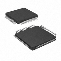


 工商网监
湘ICP备2023018690号
工商网监
湘ICP备2023018690号
