www.ti.com
Table of Contents
User’s Guide
TPS544x20 Step-Down Converter Evaluation Module
User's Guide
ABSTRACT
The PWR-634EVM evaluation module uses either the TPS544C20 or TPS544B20 devices. The TPS544C20
and TPS544B20 are highly integrated synchronous buck converters that are designed for up to 30-A or 20-A
current output, respectively.
Table of Contents
1 Description.............................................................................................................................................................................. 2
1.1 Typical Applications............................................................................................................................................................2
1.2 Features............................................................................................................................................................................. 2
2 Electrical Performance Specifications................................................................................................................................. 3
3 Schematic................................................................................................................................................................................4
4 Test Setup................................................................................................................................................................................5
4.1 Test and Configuration Software........................................................................................................................................ 5
4.2 Test Equipment.................................................................................................................................................................. 6
4.3 The PWR-634EVM.............................................................................................................................................................7
4.4 Test Set up and USB Interface Adapter............................................................................................................................. 8
4.5 List of Test Points............................................................................................................................................................... 9
5 EVM Configuration Using the Fusion GUI..........................................................................................................................10
5.1 Configuration Procedure.................................................................................................................................................. 10
6 Test Procedure...................................................................................................................................................................... 11
6.1 Line/Load Regulation and Efficiency Measurement Procedure........................................................................................11
6.2 Efficiency.......................................................................................................................................................................... 11
6.3 Equipment Shutdown....................................................................................................................................................... 11
7 Performance Data and Typical Characteristic Curves...................................................................................................... 12
7.1 Efficiency..........................................................................................................................................................................12
7.2 Load Regulation............................................................................................................................................................... 12
7.3 Transient Response......................................................................................................................................................... 13
7.4 Output Ripple................................................................................................................................................................... 14
8 Screen Shots.........................................................................................................................................................................17
8.1 Fusion GUI Screen Shots................................................................................................................................................ 17
9 EVM Assembly Drawing and PCB Layout.......................................................................................................................... 31
10 List of Materials.................................................................................................................................................................. 35
11 Revision History..................................................................................................................................................................37
SLUUAY7B – MAY 2014 – REVISED AUGUST 2021
Submit Document Feedback
TPS544x20 Step-Down Converter Evaluation Module User's Guide
Copyright © 2021 Texas Instruments Incorporated
1
�Description
www.ti.com
1 Description
The PWR-634EVM is designed as a single output DC-DC converter that demonstrates either the TPS544C20
or the TPS544B20 in a typical low-voltage application while providing a number of test points to evaluate the
performance. It uses a nominal 12-V input bus to produce a regulated 1.0-V output at up to either 30-A or 20-A
of load current, depending on the device installed.
1.1 Typical Applications
•
•
•
•
High-Density Power Solutions
Communications equipment
Servers and Computing equipment
Smart Power Systems
1.2 Features
•
•
•
2
Regulated 1.0-V output up to 30-ADC, steady-state output current
Output is marginable and trimmable via the PMBus interface.
– Programmable: UVLO, Soft Start, and Enable via the PMBus interface
– Programmable overcurrent warning and fault limits and programmable response to faults via the PMBus
interface
– Programmable overvoltage warning and fault limit and programmable response to faults via the PMBus
interface
– Programmable high- and low-output margin voltages with a maximum range of 10%, –20% of nominal
output voltage
Convenient test points for probing critical waveforms
TPS544x20 Step-Down Converter Evaluation Module User's Guide
Copyright © 2021 Texas Instruments Incorporated
SLUUAY7B – MAY 2014 – REVISED AUGUST 2021
Submit Document Feedback
�www.ti.com
Electrical Performance Specifications
2 Electrical Performance Specifications
Table 2-1. PWR-634EVM Electrical Performance Specifications
PARAMETER
TEST CONDITIONS
MIN
TYP
MAX
8
12
14
UNITS
Input Characteristics
Voltage range
VIN
Maximum input current
VIN = 8 V, IO = 30 A,
No load input current
VIN = 14 V, IO = 0 A
100
mA
1.0
V
5
V
A
Output Characteristics
VOUT
Output voltage
Output current = 10 A
IOUT
Output load current
IOUT_min to IOUT_max
Output voltage regulation
VOUT
Output voltage ripple
VOUT
Output overcurrent
0
30
Line regulation: Input voltage = 8 V to 14 V
0.5%
Load regulation: Output current = 0 A to IOUT_max
0.5%
VIN = 12 V, IOUT = 20 A
30
A
mVpp
20
A
Systems Characteristics
Switching frequency
FSW
VOUT
Peak efficiency
VIN = 8 V, IO = 10 A, FSW = 300 kHz
92%
VOUT
Full-load efficiency
VIN = 8 V, IO = 10 A, FSW = 300 kHz
90%
Operating temperature
Toper
SLUUAY7B – MAY 2014 – REVISED AUGUST 2021
Submit Document Feedback
500
kHz
105
°C
TPS544x20 Step-Down Converter Evaluation Module User's Guide
Copyright © 2021 Texas Instruments Incorporated
3
�VIN
GND
J2
VIN
2
1
VIN = 10V - 14V
VIN
10μF
470μF
TP9
C12
C23
TP8
AGND
C5
4.7μF
BP6
10μF
10μF
10μF
C15
C7
0.1μF
TP4
AGND
AGND
C14
C6
4.7μF
C13
GND
R4
DNP
Open
BP3
Output Voltage Adjust
May be used with LM10011
ADJ
TP2
20.0k
C28
33pF
1000pF
C17
GND
VOUTS+
VOUTS-
0.1μF
C16
C22
1μF
R9
30.1k
VIN
VIN
VIN
VIN
VIN
PGND
BP3
BP6
VDD
BPEXT
VOUTS+
GND
1000pF
C21
21
22
23
24
25
26
27
28
29
30
31
32
Open
DNP
C3
100k
R1
VOUTS-
0.01μF
C4
Open
DNP
C1
DNP
DNP
R7
Open C27 Open
R6
R2
DNP
Open
BP6
34
BP3
PAD
100k
R17
U1
TPS544C20RVF
39
FSW = 500KHz
R3
40
PGOOD
33
DIFFO
GND
20
FB
35
GND
18
GND
17
GND
19
COMP
36
PGOOD
38
AGND
GND
CLK
DATA
ADDR0
ADDR1
CNTL
SW
SW
SW
SW
SW
BOOT
SMBALERT
MODE
GND
37
TSNS
GND
16
Copyright © 2021 Texas Instruments Incorporated
15
TPS544x20 Step-Down Converter Evaluation Module User's Guide
14
RT
AGNDSNS
4
13
TP1
12
11
10
9
8
7
6
5
4
3
2
1
R5
TP10
0
0
R16
DNP
Open
Q1
TP3
CNTL
BP3
VOUTS-
560μF
C9
400nH
L1
TP5
C10
560μF
49.9
R15
49.9
R13
CNTL
CLK
C20
DNP
Open
TP6
VOUTS+
SMBALERT
TP12
MMBT3904
AGND
C8
0.1μF
R14
0
38.3k
38.3k
DNPC11
Open
CLK
DATA
R12
R11
R10
38.3k
Open
DNP
R8
C2
1000pF
1
3
5
7
9
SMBALERT
DATA
C19
47μF
47μF
TP11
47μF
C24
TP7
J4
1
2
J3
47μF
C25
1
2
VOUT
GND
1μF
C26
VOUT
GND
VOUT = 1.0V @ 30A MAX
2
4
6
8
10
C18
J1
Schematic
www.ti.com
3 Schematic
Figure 3-1. PWR-634EVM Schematic
SLUUAY7B – MAY 2014 – REVISED AUGUST 2021
Submit Document Feedback
�www.ti.com
Test Setup
4 Test Setup
4.1 Test and Configuration Software
To change any of the default configuration parameters on the EVM, it is necessary to obtain the TI Fusion Digital
Power Designer software. This can be downloaded from the TI website.
4.1.1 Description
The Fusion Digital Power Designer is the graphical user interface (GUI) used to configure and monitor the Texas
Instruments TPS544B20 or TPS544C20 power converter installed on this evaluation module. The application
uses the PMBus protocol to communicate with the controller over serial bus by way of a TI USB adapter (see
Figure 4-2).
4.1.2 Features
Some of the tasks you can perform with the GUI include:
•
•
•
Turn on or off the power supply output, either through the hardware control line or the PMBus operation
command.
Monitor real-time data. Items such as input voltage, output voltage, output current, temperature, and warnings
and faults are continuously monitored and displayed by the GUI.
Configure common operating characteristics such as VOUT trim and margin, UVLO, soft-start time, warning
and fault thresholds, fault response, and ON/OFF.
This software is available for download at http://www.ti.com/tool/fusion_digital_power_designer
SLUUAY7B – MAY 2014 – REVISED AUGUST 2021
Submit Document Feedback
TPS544x20 Step-Down Converter Evaluation Module User's Guide
Copyright © 2021 Texas Instruments Incorporated
5
�Test Setup
www.ti.com
4.2 Test Equipment
Voltage Source: The input voltage source VIN must be a 0-V to 14-V variable dc source capable of supplying at
least 5 Adc. Connect VIN to J2 Figure 4-1.
Multimeters: It is recommended to use two separate multimeters Figure 4-1. One meter is used to measure Vin
and one to measure Vout.
Output Load: A variable electronic load is recommended for testing Figure 4-1. It must be capable of 30 A at
voltages as low as 0.9 V.
Oscilloscope: An oscilloscope is recommended for measuring output noise and ripple. Output ripple must be
measured using a Tip-and-Barrel method or better as shown in Figure 4-3.The scope must be adjusted to
20-MHz bandwidth, ac coupling at 50 mV/division, and must be set to 1-µs/division.
Fan: During prolonged operation at high loads, it may be necessary to provide forced air cooling with a small fan
aimed at the EVM. Temperature of the devices on the EVM must be maintained below 105°C.
USB-to-GPIO Interface Adapter: A communications adapter is required between the EVM and the host
computer. This EVM was designed to use the Texas Instruments USB-to-GPIO Adapter (see Figure 4-2). This
adapter can be purchased at http://www.ti.com/tool/usb-to-gpio.
Recommended Wire Gauge: The voltage drop in the load wires must be kept as low as possible in order to
keep the working voltage at the load within its operating range. See the following table for recommended wire
gauge and length to achieve a voltage drop of no more than 0.2 V at the maximum 30-A load.
AWG GAUGE
Ω PER FOOT
(Ω)
LOAD WIRES COMBINED
LENGTH
(Ft)
EACH WIRE LENGTH
(Ft)
12
1.59E-3
6.30
3.15
14
2.53E-3
3.96
1.98
16
4.02E-3
2.49
1.25
18
6.39E-3
1.57
0.78
As an example, if AWG 12 wire is used, no more than 3.15 feet of wire must be used between the EVM and the
load.
6
TPS544x20 Step-Down Converter Evaluation Module User's Guide
Copyright © 2021 Texas Instruments Incorporated
SLUUAY7B – MAY 2014 – REVISED AUGUST 2021
Submit Document Feedback
�www.ti.com
Test Setup
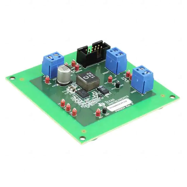
4.3 The PWR-634EVM
Figure 4-1. PWR-634EVM Overview
SLUUAY7B – MAY 2014 – REVISED AUGUST 2021
Submit Document Feedback
TPS544x20 Step-Down Converter Evaluation Module User's Guide
Copyright © 2021 Texas Instruments Incorporated
7
�Test Setup
www.ti.com
4.4 Test Set up and USB Interface Adapter
Figure 4-2. Complete Test Setup Including Texas Instruments USB-to-GPIO Adapter
Metal Ground
Barrel
Probe
Tip
Tip and Barrel VOUT Ripple
Measurement
Figure 4-3. Tip and Barrel Measurement
8
TPS544x20 Step-Down Converter Evaluation Module User's Guide
Copyright © 2021 Texas Instruments Incorporated
SLUUAY7B – MAY 2014 – REVISED AUGUST 2021
Submit Document Feedback
�www.ti.com
Test Setup
4.5 List of Test Points
Table 4-1. The Function of Each Test Point
TEST POINT
TYPE
NAME
TP1
T-H loop
PGOOD
TP2
T-H loop
ADJ
TP3
T-H loop
SMBALERT
SMB alert signal
TP4
T-H loop
BPEXT
Bypass connect
TP5
T-H loop
VOUT + Sense
TP6
T-H loop
VOUT – Sense
TP7
T-H loop
VOUT+
TP8
T-H loop
VIN+
TP9
T-H loop
VIN–
TP10
T-H loop
GND
TP11
T-H loop
VOUT–
TP12
T-H loop
CNTL
SLUUAY7B – MAY 2014 – REVISED AUGUST 2021
Submit Document Feedback
DESCRIPTION
Power good signal for VOUT.
Output voltage adjust
Control signal
TPS544x20 Step-Down Converter Evaluation Module User's Guide
Copyright © 2021 Texas Instruments Incorporated
9
�EVM Configuration Using the Fusion GUI
www.ti.com
5 EVM Configuration Using the Fusion GUI
The TPS544B20 or TPS544C20 installed on this EVM leave the factory pre-configured. See Table 5-1 for a short
list of key factory configuration parameters as obtained from the configuration file.
Table 5-1. Key Factory Configuration Parameters
ADDRESS HEX
0x1B
ADDRESS DEC
PART ID
27
TPS544x20
GENERAL
CMD ID WITH PHASE
CMD CODE HEX
ENCODED HEX
DECODED
NUMERIC
VIN_OFF
0x36
0xF014
5.00 V
5
Turn OFF voltage
VIN_ON
0x35
0xF01C
7.00 V
7
Turn ON voltage
TPS544B20
COMMENTS
COMMENTS
IOUT_CAL_GAIN
0x38
0x8821
1.0071 mΩ
1.0071
IOUT_CAL_OFFSET
0x39
0xE000
0.0000 A
0
DCR of output inductor
Current offset for GUI readout
IOUT_OC_FAULT_LIMIT
0x46
0xF83C
30.0 A
30
OC fault level
IOUT_OC_FAULT_RESPONSE
0x47
0x3C
Restart continuously
IOUT_OC_WARN_LIMIT
0x4A
0xF832
25.0 A
25
OC warning level
MFR_04 (VREF_TRIM)
0xD4
0x0000
0.000 V
0
Trim voltage
ON_OFF_CONFIG
0x02
0x02
Mode: always converting
Response to OC fault
Control signal and operation command not
required
OPERATION
0x01
0x00
Unit: immediate off; margin: none
OT_FAULT_LIMIT
0x4F
0x007D
125°C
125
Response to turn OFF trigger
OT fault level
OT_WARN_LIMIT
0x51
0x0064
100°C
100
OT warn level
TON_RISE
0x61
0xE02B
2.6875 ms
2.6875
Soft-start time
TPS544C20
COMMENTS
IOUT_CAL_GAIN
0x38
0x8821
1.0071 mΩ
1.0071
IOUT_CAL_OFFSET
0x39
0xE000
0.0000 A
0
DCR of output inductor
Current offset for GUI readout
IOUT_OC_FAULT_LIMIT
0x46
0xF832
25.0 A
25
OC fault level
IOUT_OC_FAULT_RESPONSE
0x47
0x3C
Restart continuously
IOUT_OC_WARN_LIMIT
0x4A
0xF828
20.0 A
20
OC warning level
MFR_04 (VREF_TRIM)
0xD4
0x0000
0.000 V
0
Trim voltage
ON_OFF_CONFIG
0x02
0x02
Mode: always converting
Response to OC fault
Control signal and operation command not
required
OPERATION
0x01
0x00
Unit: immediate off; margin: none
OT_FAULT_LIMIT
0x4F
0x007D
125°C
125
Response to turn off trigger
OT fault level
OT_WARN_LIMIT
0x51
0x0064
100°C
100
OT warn level
TON_RISE
0x61
0xE02B
2.6875 ms
2.6875
Soft-start time
If it is desired to configure the EVM to settings other than the factory settings shown in Table 5-1, the TI Fusion
Digital Power Designer software can be used for reconfiguration. It is necessary to have input voltage applied
to the EVM prior to launching the software so that the TPS544B20 or TPS544C20 installed is active and able
to respond to the GUI and the GUI can recognize the device. The default configuration for the EVM is to start
converting at an input voltage of 4.5 V; therefore, to avoid any converter activity during configuration, an input
voltage less than 4.5 V must be applied. An input voltage of 4 V is recommended.
5.1 Configuration Procedure
1.
2.
3.
4.
10
Adjust the input supply to provide 4 VDC, current limited to 1 A.
Apply the input voltage to the EVM. See Figure 4-1 and Figure 4-2 for connections and test setup.
Launch the Fusion GUI software. See the screen shots in Section 8 for more information.
Configure the EVM operating parameters as desired.
TPS544x20 Step-Down Converter Evaluation Module User's Guide
Copyright © 2021 Texas Instruments Incorporated
SLUUAY7B – MAY 2014 – REVISED AUGUST 2021
Submit Document Feedback
�www.ti.com
Test Procedure
6 Test Procedure
6.1 Line/Load Regulation and Efficiency Measurement Procedure
1.
2.
3.
4.
5.
Set up the EVM as described in Section 4.3 and Figure 4-1.
Ensure that the electronic load is set to draw 0 ADC.
Increase VIN from 0 V to 12 V using the DMM to measure input voltage.
Use the other DMM to measure output voltage VOUT.
Vary the load from 0 ADC to maximum rated output ADC (TPS544B20 = 20 A, TPS544C20 = 30 A). VOUT
must remain in regulation as defined in Table 2-1.
6. Vary VIN from 8 V to 14 V. VOUT must remain in regulation as defined in Table 2-1.
7. Decrease the load to 0 A.
8. Decrease VIN to 0 V.
6.2 Efficiency
To measure the efficiency of the power train on the EVM, it is important to measure the voltages at the correct
location. This is necessary because otherwise the measurements will include losses in efficiency that are not
related to the power train itself. Losses incurred by the voltage drop in the copper traces and in the input and
output connectors are not related to the efficiency of the power train, and they must not be included in efficiency
measurements.
Table 6-1. List of Test Points for Efficiency Measurements
TEST POINT
NODE NAME
DESCRIPTION
TP8
VIN
Measurement point for VIN +VE
TP9
PGND
Measurement point for VIN –VE
TP7
VOUT
Measurement point for VOUT +VE
TP11
PGND
Measurement point for VOUT –VE
Input current can be measured at any point in the input wires, and output current can be measured anywhere
in the output wires of the output being measured. Using these measurement points result in efficiency
measurements that do not include losses due to the connectors and PCB traces.
6.3 Equipment Shutdown
1.
2.
3.
4.
Reduce the load current on both outputs to 0 A.
Reduce input voltage to 0 V.
Shut down the external fan if in use.
Shut down equipment.
SLUUAY7B – MAY 2014 – REVISED AUGUST 2021
Submit Document Feedback
TPS544x20 Step-Down Converter Evaluation Module User's Guide
Copyright © 2021 Texas Instruments Incorporated
11
�Performance Data and Typical Characteristic Curves
www.ti.com
7 Performance Data and Typical Characteristic Curves
Figure 7-1 through Figure 7-9 present typical performance curves for the PWR-634EVM.
7.1 Efficiency
100.0
90.0
80.0
70.0
60.0
8V
50.0
12V
40.0
14V
30.0
20.0
10.0
0.0
1 2 3 4 5 6 7 8 9 101112131415161718192021222324
Figure 7-1. Efficiency of 1-V Output vs Line and Load
7.2 Load Regulation
1.014
1.012
1.010
1.008
8V
12V
1.006
14V
1.004
1.002
1.000
1 2 3 4 5 6 7 8 9 101112131415161718192021222324
Figure 7-2. Load Regulation of 1-V Output
12
TPS544x20 Step-Down Converter Evaluation Module User's Guide
Copyright © 2021 Texas Instruments Incorporated
SLUUAY7B – MAY 2014 – REVISED AUGUST 2021
Submit Document Feedback
�www.ti.com
Performance Data and Typical Characteristic Curves
7.3 Transient Response
Ch1 = VOUT1 at 50-mV/division, Ch2 = IOUT1 at 5-A/division
Figure 7-3. Transient Response of 1-V Output at 12 VIN, Transient is 10 A to 20 A
Ch1 = VOUT1 at 50-mV/division, Ch2 = IOUT1 at 5-A/division
Figure 7-4. Transient Response of 1-V Output at 12 VIN, Transient is 20 A to 10 A
SLUUAY7B – MAY 2014 – REVISED AUGUST 2021
Submit Document Feedback
TPS544x20 Step-Down Converter Evaluation Module User's Guide
Copyright © 2021 Texas Instruments Incorporated
13
�Performance Data and Typical Characteristic Curves
www.ti.com
7.4 Output Ripple
Ch1 = VOUT1 at 20-mV/division, Ch2 = SW Node at 10-V/division
Figure 7-5. Output Ripple and SW Node of 1-V Output at 12 VIN, 1-A Output
Ch1 = VOUT1 at 20-mV/division, Ch2 = SW Node at 10-V/division
Figure 7-6. Output Ripple and SW Node of 1-V Output at 12 VIN, 20-A Output
14
TPS544x20 Step-Down Converter Evaluation Module User's Guide
Copyright © 2021 Texas Instruments Incorporated
SLUUAY7B – MAY 2014 – REVISED AUGUST 2021
Submit Document Feedback
�www.ti.com
Performance Data and Typical Characteristic Curves
Ch1 = VOUT2 at 20-mV/division, Ch2 = SW Node at 10-V/division
Figure 7-7. Start up from Control 1-V Output at 12 VIN, 20-A Output
Ch1 = VOUT2 at 20-mV/division, Ch2 = SW Node at 10-V/division
Figure 7-8. Shutdown from Control and SW Node of 1-V Output at 12 VIN, 20-A Output
SLUUAY7B – MAY 2014 – REVISED AUGUST 2021
Submit Document Feedback
TPS544x20 Step-Down Converter Evaluation Module User's Guide
Copyright © 2021 Texas Instruments Incorporated
15
�Performance Data and Typical Characteristic Curves
www.ti.com
Figure 7-9. 50% PreBias Start (No Load)
16
TPS544x20 Step-Down Converter Evaluation Module User's Guide
Copyright © 2021 Texas Instruments Incorporated
SLUUAY7B – MAY 2014 – REVISED AUGUST 2021
Submit Document Feedback
�www.ti.com
Screen Shots
8 Screen Shots
8.1 Fusion GUI Screen Shots
Figure 8-1. First Window at Fusion Launch
Device Found
Figure 8-2. Scan Finds Device Successfully
SLUUAY7B – MAY 2014 – REVISED AUGUST 2021
Submit Document Feedback
TPS544x20 Step-Down Converter Evaluation Module User's Guide
Copyright © 2021 Texas Instruments Incorporated
17
�Screen Shots
www.ti.com
Figure 8-3. Software Launch Continued
Figure 8-4. Software Launch Continued
18
TPS544x20 Step-Down Converter Evaluation Module User's Guide
Copyright © 2021 Texas Instruments Incorporated
SLUUAY7B – MAY 2014 – REVISED AUGUST 2021
Submit Document Feedback
�www.ti.com
Screen Shots
Use this next screen to configure the following (Figure 8-5):
•
•
•
•
•
•
•
•
OC fault and OC warn
OT fault and OT warn
Power good limits
Fault response
UVLO
On/Off configuration
Soft-start time
Margin voltage
Figure 8-5. First Screen After Successful Launch: Configure- Limits & On/Off
SLUUAY7B – MAY 2014 – REVISED AUGUST 2021
Submit Document Feedback
TPS544x20 Step-Down Converter Evaluation Module User's Guide
Copyright © 2021 Texas Instruments Incorporated
19
�Screen Shots
www.ti.com
Use this screen to configure the following (Figure 8-6) :
•
•
VREF trim
IOUT cal gain (DCR of output choke)
Figure 8-6. Configure – Other
Use this screen to configure all of the configurable parameters (Figure 8-7). The screen also shows other details,
like hexadecimal (hex) encoding.
Figure 8-7. Configure – All
20
TPS544x20 Step-Down Converter Evaluation Module User's Guide
Copyright © 2021 Texas Instruments Incorporated
SLUUAY7B – MAY 2014 – REVISED AUGUST 2021
Submit Document Feedback
�www.ti.com
Screen Shots
Changing the on/off configuration prompts a pop-up window with details of the options Figure 8-8).
Figure 8-8. Configure- Limits and On/Off- On/Off Configuration Pop-up
After a change is selected, an orange U icon is displayed to offer the Undo Change option. The change is not
retained until either Write to Hardware or Store User Defaults is selected. When Write to Hardware is selected,
the change is committed to volatile memory and defaults back to the previous setting on the input power cycle.
When Store User Defaults is selected, the change is committed to the nonvolatile memory and becomes the new
default (Figure 8-9).
Figure 8-9. Configure- Limits and On/Off- On/Off Config Pop-up
SLUUAY7B – MAY 2014 – REVISED AUGUST 2021
Submit Document Feedback
TPS544x20 Step-Down Converter Evaluation Module User's Guide
Copyright © 2021 Texas Instruments Incorporated
21
�Screen Shots
www.ti.com
The IOUT cal gain can be typed in or scrolled to a new value. The range for IOUT cal gain is 0.244 mΩ to 15.5 mΩ
and the resolution step is 30.5 µΩ. If a value is typed in that is between the available discrete steps, the typed-in
value does not change but the nearest discrete step is retained. The actual step is displayed on relaunch of the
Fusion GUI (Figure 8-10).
Figure 8-10. Configure- Other- IOUT Cal Gain Change
The On/Off configuration can also be configured from the All configuration screens, where the same process
applies (Figure 8-11).
Figure 8-11. Configure- All Config- On/Off Config Pop-up
22
TPS544x20 Step-Down Converter Evaluation Module User's Guide
Copyright © 2021 Texas Instruments Incorporated
SLUUAY7B – MAY 2014 – REVISED AUGUST 2021
Submit Document Feedback
�www.ti.com
Screen Shots
After making changes to one or more configurable parameters, the changes can be committed to nonvolatile
memory by selecting Store User Defaults. This action prompts a confirm selection pop-up, and if confirmed, the
changes are committed to nonvolatile memory (Figure 8-12).
Figure 8-12. Configure- Store User Defaults
In the lower left corner, the different view screens can be changed. The view screens can be changed between
Configure, Monitor and Status as needed (Figure 8-13).
Figure 8-13. Change View Screen to Monitor Screen
SLUUAY7B – MAY 2014 – REVISED AUGUST 2021
Submit Document Feedback
TPS544x20 Step-Down Converter Evaluation Module User's Guide
Copyright © 2021 Texas Instruments Incorporated
23
�Screen Shots
www.ti.com
When the Monitor screen is selected (Figure 8-14), the screen changes to display real-time data of the
parameters that are measured by the controller. This screen provides access to:
•
•
•
•
•
•
•
Graphs of VOUT, IOUT, Temperature, and POUT. As shown, POUT display is turned off.
Start/Stop polling which turns on or off the real-time display of data.
Quick access to on/off configuration
Control pin activation, and operation command. As shown, because the device is configured for always
converting, these radio buttons are either grayed-out or have no effect.
Margin control
PMBus log, which displays activity on the PMBus
Tips and hints, which displays additional information when the cursor is hovered over configurable
parameters.
At first GUI launch, faults can occur due to communications during power up. These faults can be cleared once
the device is enabled.
Figure 8-14. Monitor Screen
24
TPS544x20 Step-Down Converter Evaluation Module User's Guide
Copyright © 2021 Texas Instruments Incorporated
SLUUAY7B – MAY 2014 – REVISED AUGUST 2021
Submit Document Feedback
�www.ti.com
Screen Shots
Selecting System Dashboard from the mid-left screen adds a new window which displays system-level
information (Figure 8-15).
Figure 8-15. System Dashboard
When the EVM starts converting power, the VOUT graph changes scale to display both the zero and VOUT level.
Once the EVM is converting and clear of any faults, selecting Clear Faults clears any prior fault flags (Figure
8-16).
Figure 8-16. Display Change on Power Up
SLUUAY7B – MAY 2014 – REVISED AUGUST 2021
Submit Document Feedback
TPS544x20 Step-Down Converter Evaluation Module User's Guide
Copyright © 2021 Texas Instruments Incorporated
25
�Screen Shots
www.ti.com
Selecting Clear Faults clears any prior fault flags. Scrolling time window of VOUT will still show any turn-on event
(Figure 8-17).
Figure 8-17. Faults Cleared
Selecting Status from lower left corner shows the status of the controller (Figure 8-18).
Figure 8-18. Status Screen
26
TPS544x20 Step-Down Converter Evaluation Module User's Guide
Copyright © 2021 Texas Instruments Incorporated
SLUUAY7B – MAY 2014 – REVISED AUGUST 2021
Submit Document Feedback
�www.ti.com
Screen Shots
Selecting the pulldown menu File- Import Project from the upper left menu bar can be used to configure
all parameters in the device at once with a desired configuration, or even revert back to a known-good
configuration. This action results in a browse-type sequence where the desired configuration file can be located
and loaded (Figure 8-19).
Figure 8-19. Import Project / Import Configuration File
Selecting Store User Configuration to Flash Memory from the device pulldown menu has the same functionality
as the Store User Defaults button from within the configure screen. It results in committing the current
configuration to nonvolatile memory (Figure 8-20).
Figure 8-20. Store Configuration To Memory
SLUUAY7B – MAY 2014 – REVISED AUGUST 2021
Submit Document Feedback
TPS544x20 Step-Down Converter Evaluation Module User's Guide
Copyright © 2021 Texas Instruments Incorporated
27
�Screen Shots
www.ti.com
Select Data Logging (Figure 8-21), from the Tools drop-down menu. This enables logging of common operating
values such as VOUT, IOUT, and temperature. The user is prompted to select a location for the file to be stored
as well as the type of file. Select the storage location for the file and the type of file. The file will be a CSV file to
be stored in the directory path shown. Logging begins when the Start Data Logging button is selected, and stops
when it is reselected.
Figure 8-21. Data Logging Details
Common contents of the data log as shown in (Figure 8-22). The UUT had was running with a modified voltage,
at an approximate 3.5-A load and room temperature.
Figure 8-22. Data Log File
28
TPS544x20 Step-Down Converter Evaluation Module User's Guide
Copyright © 2021 Texas Instruments Incorporated
SLUUAY7B – MAY 2014 – REVISED AUGUST 2021
Submit Document Feedback
�www.ti.com
Screen Shots
Selecting PMBus Logging (Figure 8-23) from the Tools drop-down menu enables the logging of all PMBus
activity in the same way as the datalogging. This includes communications traffic for each polling loop between
the GUI and the device. It also includes common operating values such as VOUT, IOUT, and temperature. The
user is prompted to select a location for the file to be stored. See the next screen (Figure 8-24).
Figure 8-23. PMBus Logging
SLUUAY7B – MAY 2014 – REVISED AUGUST 2021
Submit Document Feedback
TPS544x20 Step-Down Converter Evaluation Module User's Guide
Copyright © 2021 Texas Instruments Incorporated
29
�Screen Shots
www.ti.com
Select the storage location for the file and the type of file. As shown (Figure 8-24), the file is a CSV file to be
stored in the directory path shown. Logging begins when the Start Logging button is selected, and stops when it
is reselected (as Stop Logging). This file can rapidly grow in size, so caution is advised when using this function.
Figure 8-24. PMBus Log Details
Data is stored in a CSV file, with a date-stamp name (Figure 8-25).
Figure 8-25. PMBus Log
30
TPS544x20 Step-Down Converter Evaluation Module User's Guide
Copyright © 2021 Texas Instruments Incorporated
SLUUAY7B – MAY 2014 – REVISED AUGUST 2021
Submit Document Feedback
�www.ti.com
EVM Assembly Drawing and PCB Layout
9 EVM Assembly Drawing and PCB Layout
Figure 9-1 through Figure 9-5 show the design of the PWR-634EVM printed-circuit board (PCB).
Figure 9-1. PWR-634EVM Top Layer Assembly Drawing (Top View)
Figure 9-2. PWR-634EVM Top Copper
SLUUAY7B – MAY 2014 – REVISED AUGUST 2021
Submit Document Feedback
TPS544x20 Step-Down Converter Evaluation Module User's Guide
Copyright © 2021 Texas Instruments Incorporated
31
�EVM Assembly Drawing and PCB Layout
www.ti.com
Figure 9-3. PWR-634EVM Layer 1 (Top View)
Figure 9-4. PWR-634EVM Layer 2 (Top View)
32
TPS544x20 Step-Down Converter Evaluation Module User's Guide
Copyright © 2021 Texas Instruments Incorporated
SLUUAY7B – MAY 2014 – REVISED AUGUST 2021
Submit Document Feedback
�www.ti.com
EVM Assembly Drawing and PCB Layout
Figure 9-5. PWR-634EVM Layer 3 (Top View)
Figure 9-6. PWR-634EVM Layer 4 (Top View)
SLUUAY7B – MAY 2014 – REVISED AUGUST 2021
Submit Document Feedback
TPS544x20 Step-Down Converter Evaluation Module User's Guide
Copyright © 2021 Texas Instruments Incorporated
33
�EVM Assembly Drawing and PCB Layout
www.ti.com
Figure 9-7. PWR-634EVM Bottom Copper (Top X-ray View)
Figure 9-8. PWR-634EVM Bottom Assembly (Top X-ray View)
34
TPS544x20 Step-Down Converter Evaluation Module User's Guide
Copyright © 2021 Texas Instruments Incorporated
SLUUAY7B – MAY 2014 – REVISED AUGUST 2021
Submit Document Feedback
�www.ti.com
List of Materials
10 List of Materials
Table 10-1 lists the EVM components list according to Figure 3-1.
Note
The TPS544C20 version is used for this example.
Table 10-1. PWR091 List of Materials
DES
QTY
DESCRIPTION
PART NUMBER
MANUFACTURER
C2, C17, C21
3
Capacitor, ceramic, 1000 pF, 50 V, ±10%, X7R, 0402
C1005X7R1H102K
TDK
C4
1
Capacitor, ceramic, 0.01 µF, 25 V, ±10%, X7R, 0402
C1005X7R1E103K
TDK
C5
1
Capacitor, ceramic, 4.7 µF, 16 V, ±10%, X5R, 0603
GRM188R61C475KAA MuRata
J
C6
1
Capacitor, ceramic, 4.7 µF, 10 V, ±20%, X5R, 0402
GRM155R61A475M
C7
1
Capacitor, ceramic, 0.1 µF, 10 V, ±10%, X5R, 0402
GRM155R61A104KA0 MuRata
1D
C8, C16
2
Capacitor, ceramic, 0.1 µF, 25 V, ±5%, X7R, 0603
C0603C104J3RACTU
Kemet
C9, C10
2
Capacitor, TA, 560uF, 2 V, +/-10%, 0.005 Ω, SMD
2TPLF560M5
Sanyo
C12, C13, C14,
C15
4
Capacitor, ceramic, 10 µF, 25 V, ±10%, X7R, 1206
GRM31CR71E106KA1 MuRata
2L
C18, C19, C24,
C25
4
Capacitor, ceramic, 47 µF, 6.3 V, ±20%, X5R, 0805
JMK212BJ476MG-T
C22, C26
2
Capacitor, ceramic, 1 µF, 25 V, ±10%, X5R, 0402
C1005X5R1E105K050 TDK
BC
C23
1
Capacitor, aluminum, 470 µF, 16 V, ±20%, Ω, SMD
EMVA160ADA471MH
A0G
Nippon Chemi-Con
C1, C3
0
Capacitor, ceramic, 0.01 µF, 25 V, ±10%, X7R, 0402
C1005X7R1E103K
TDK
C11
0
Capacitor, ceramic, 1000 pF, 50 V, ±10%, X7R, 0402
C1005X7R1H102K
TDK
C20
1
Capacitor, ceramic, 120 pF, 50 V, ±5%, C0G/NP0, 0402
C1005C0G1H121J
TDK
C27
0
Capacitor, ceramic, 1000 pF, 50 V, ±10%, X7R, 0402
C1005X7R1H102K
TDK
C28
1
Capacitor, ceramic, 33 pF, 50 V, ±10%, C0G, 0402
C1005X7R1H330K
TDK
FID1, FID2,
FID3
0
Fiducial mark. There is nothing to buy or mount.
N/A
N/A
H1, H2, H3, H4
4
Bumpon, hemisphere, 0.44 × 0.20, clear
SJ-5303 (CLEAR)
3M
J1
1
Header (shrouded), 100 mil, 5 × 2, gold, TH
5103308-1
TE Connectivity
J2, J3, J4
3
Terminal block 5.08 mm vert 2 pos
ED120/2DS
On-Shore Technology
L1
1
Inductor, Shielded, Composite, 400 nH, 36.8A, 0.0004 Ω,
SMD
XAL1060-401MEB
Coilcraft
LBL1
1
Thermal transfer printable labels, 0.650" W x 0.200" H 10,000 per roll
THT-14-423-10
Brady
!PCB
1
Printed circuit board
PWR634
Any
Q1
1
Transistor, NPN, 40 V, 0.2 A, SOT-23
MMBT3904
Fairchild
Semiconductor
SLUUAY7B – MAY 2014 – REVISED AUGUST 2021
Submit Document Feedback
MuRata
Taiyo Yuden
TPS544x20 Step-Down Converter Evaluation Module User's Guide
Copyright © 2021 Texas Instruments Incorporated
35
�List of Materials
www.ti.com
Table 10-1. PWR091 List of Materials (continued)
DES
QTY
DESCRIPTION
PART NUMBER
MANUFACTURER
R1, R17
2
Resistor, 100 kΩ, 1%, 0.063 W, 0402
CRCW0402100KFKE
D
R3, R10, R14
3
Resistor, 0 Ω, 5%, 0.063 W, 0402
CRCW04020000Z0ED Vishay-Dale
R6
1
Resistor, 20.0 kΩ, 1%, 0.063 W, 0402
CRCW040220K0FKE
D
Vishay-Dale
R13, R15, R18
3
Resistor, 49.9 Ω, 1%, 0.063 W, 0402
CRCW040249R9FKE
D
Vishay-Dale
R9
1
Resistor, 30.1 kΩ, 1%, 0.063 W, 0402
CRCW040230K1FKE
D
Vishay-Dale
R2, R4
0
Resistor, 20.0 kΩ, 1%, 0.063 W, 0402
CRCW040220K0FKE
D
Vishay-Dale
R5
0
Resistor, 0 Ω, 5%, 0.063 W, 0402
CRCW04020000Z0ED Vishay-Dale
R16
0
Resistor, 1.0 Ω, 5%, 0.25 W, 1206
CRCW12061R00JNEA Vishay-Dale
R8, R11, R12
3
Resistor, 38.3 kΩ, 1%, 0.063 W, 0402
CRCW040238K3FKE
D
Vishay-Dale
TP1, TP2, TP3,
TP4, TP5, TP6,
TP7, TP8, TP12
11
Test point, miniature, red, TH
5000
Keystone
TP9, TP10,
TP11
3
Test point, miniature, black, TH
5001
Keystone
U1
1
TPS544C20 18-V, 30-A PMBus Synchronous Buck
Converters, RVF0040A
TPS544C20RVF
Texas Instruments
36
TPS544x20 Step-Down Converter Evaluation Module User's Guide
Copyright © 2021 Texas Instruments Incorporated
Vishay-Dale
SLUUAY7B – MAY 2014 – REVISED AUGUST 2021
Submit Document Feedback
�www.ti.com
Revision History
11 Revision History
NOTE: Page numbers for previous revisions may differ from page numbers in the current version.
Changes from Revision A (June 2014 August 2021) to Revision B ()
Page
• Changed user's guide title.................................................................................................................................. 2
• Updated the numbering format for tables, figures, and cross-references throughout the document. ................2
• Edited user's guide for clarity .............................................................................................................................2
Changes from Revision * (May 2014) to Revision A (June 2014)
Page
• Added updated PWR-634EVM Schematic drawings..........................................................................................4
• Added updated EVM Assembly Drawings and PCB Layout drawings............................................................. 31
• Changed List of Materials................................................................................................................................. 35
SLUUAY7B – MAY 2014 – REVISED AUGUST 2021
Submit Document Feedback
TPS544x20 Step-Down Converter Evaluation Module User's Guide
Copyright © 2021 Texas Instruments Incorporated
37
�IMPORTANT NOTICE AND DISCLAIMER
TI PROVIDES TECHNICAL AND RELIABILITY DATA (INCLUDING DATA SHEETS), DESIGN RESOURCES (INCLUDING REFERENCE
DESIGNS), APPLICATION OR OTHER DESIGN ADVICE, WEB TOOLS, SAFETY INFORMATION, AND OTHER RESOURCES “AS IS”
AND WITH ALL FAULTS, AND DISCLAIMS ALL WARRANTIES, EXPRESS AND IMPLIED, INCLUDING WITHOUT LIMITATION ANY
IMPLIED WARRANTIES OF MERCHANTABILITY, FITNESS FOR A PARTICULAR PURPOSE OR NON-INFRINGEMENT OF THIRD
PARTY INTELLECTUAL PROPERTY RIGHTS.
These resources are intended for skilled developers designing with TI products. You are solely responsible for (1) selecting the appropriate
TI products for your application, (2) designing, validating and testing your application, and (3) ensuring your application meets applicable
standards, and any other safety, security, regulatory or other requirements.
These resources are subject to change without notice. TI grants you permission to use these resources only for development of an
application that uses the TI products described in the resource. Other reproduction and display of these resources is prohibited. No license
is granted to any other TI intellectual property right or to any third party intellectual property right. TI disclaims responsibility for, and you
will fully indemnify TI and its representatives against, any claims, damages, costs, losses, and liabilities arising out of your use of these
resources.
TI’s products are provided subject to TI’s Terms of Sale or other applicable terms available either on ti.com or provided in conjunction with
such TI products. TI’s provision of these resources does not expand or otherwise alter TI’s applicable warranties or warranty disclaimers for
TI products.
TI objects to and rejects any additional or different terms you may have proposed. IMPORTANT NOTICE
Mailing Address: Texas Instruments, Post Office Box 655303, Dallas, Texas 75265
Copyright © 2022, Texas Instruments Incorporated
�


 工商网监
湘ICP备2023018690号
工商网监
湘ICP备2023018690号
