Typical Size
6,6 mm X 9,8 mm
www.ti.com
TPS54611-EP, TPS54612-EP
TPS54613-EP, TPS54614-EP
TPS54615-EP, TPS54616-EP
SGLS293A – FEBRUARY 2005 – REVISED AUGUST 2005
3-V TO 6-V INPUT, 6-A OUTPUT SYNCHRONOUS BUCK PWM
SWITCHER WITH INTEGRATED FETs (SWIFT™)
FEATURES
APPLICATIONS
•
•
•
•
•
•
•
•
•
•
•
•
•
(1)
Controlled Baseline
– One Assembly/Test Site, One Fabrication
Site
Extended Temperature Performance of –55°C
to 125°C
Enhanced Diminishing Manufacturing
Sources (DMS) Support
Enhanced Product-Change Notification
Qualification Pedigree (1)
30-mΩ, 12-A Peak MOSFET Switches for High
Efficiency at 6-A Continuous Output Source
and Sink
0.9-V, 1.2-V, 1.5-V, 1.8-V, 2.5-V, and 3.3-V
Fixed Output Voltage Devices With 1% Initial
Accuracy
Internally Compensated for Easy Use and
Minimal Component Count
Fast Transient Response
Wide PWM Frequency - Fixed 350 kHz,
550 kHz or Adjustable 280 kHz to 700 kHz
Load Protected by Peak Current Limit and
Thermal Shutdown
Integrated Solution Reduces Board Area and
Total Cost
Component qualification in accordance with JEDEC and
industry standards to ensure reliable operation over an
extended temperature range. This includes, but is not limited
to, Highly Accelerated Stress Test (HAST) or biased 85/85,
temperature cycle, autoclave or unbiased HAST,
electromigration, bond intermetallic life, and mold compound
life. Such qualification testing should not be viewed as
justifying use of this component beyond specified
performance and environmental limits.
•
•
•
Low-Voltage, High-Density Systems With
Power Distributed at 5 V or 3.3 V
Point of Load Regulation for High
Performance DSPs, FPGAs, ASICs and
Microprocessors
Broadband, Networking and Optical
Communications Infrastructure
Portable Computing/Notebook PCs
DESCRIPTION
The SWIFT™ family of dc/dc regulators, the
TPS54611, TPS54612, TPS54613, TPS54614,
TPS54615, and TPS54616 low-input voltage
high-output
current
synchronous-buck
PWM
converters integrate all required active components.
Included on the substrate are true, high-performance,
voltage error amplifiers that provide high performance
under transient conditions; an under-voltage lockout
circuit to prevent start-up until the input voltage
reaches 3 V; an internally and externally set
slow-start circuit to limit in-rush currents; and a power
good output useful for processor/logic reset, fault
signaling, and supply sequencing.
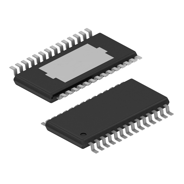
The TPS54611-6 devices are available in a thermally
enhanced 28-pin TSSOP (PWP) PowerPAD™
package, which eliminates bulky heatsinks. Texas
Instruments provides evaluation modules and the
SWIFT™ designer software tool to aid in quickly
achieving high-performance power supply designs to
meet aggressive equipment development cycles.
These devices have limited built-in ESD protection. The leads should be shorted together or the device
placed in conductive foam during storage or handling to prevent electrostatic damage to the MOS gates.
Please be aware that an important notice concerning availability, standard warranty, and use in critical applications of Texas
Instruments semiconductor products and disclaimers thereto appears at the end of this data sheet.
SWIFT, PowerPAD are trademarks of Texas Instruments.
PRODUCTION DATA information is current as of publication date.
Products conform to specifications per the terms of the Texas
Instruments standard warranty. Production processing does not
necessarily include testing of all parameters.
Copyright © 2005, Texas Instruments Incorporated
�TPS54611-EP, TPS54612-EP
TPS54613-EP, TPS54614-EP
TPS54615-EP, TPS54616-EP
www.ti.com
SGLS293A – FEBRUARY 2005 – REVISED AUGUST 2005
EFFICIENCY AT 350 kHz
100
SIMPLIFIED SCHEMATIC
95
Output
Input
90
PH
TPS54614
BOOT
85
Efficiency − %
VIN
PGND
VBIAS VSENSE
AGND
80
75
70
65
60
55
50
0
1
2
3
4
5
6
Load Current − A
PWP PACKAGE
(TOP VIEW)
AGND
VSENSE
NC
PWRGD
BOOT
PH
PH
PH
PH
PH
PH
PH
PH
PH
1
2
3
4
5
6
7
8
9
10
11
12
13
14
28
27
26
25
24
23
THERMAL 22
PAD
21
20
19
18
17
16
15
RT
FSEL
SS/ENA
VBIAS
VIN
VIN
VIN
VIN
VIN
PGND
PGND
PGND
PGND
PGND
AVAILABLE OPTIONS
PACKAGED DEVICES
TJ
–55°C to 125°C
(1)
(2)
2
OUTPUT VOLTAGE
PLASTIC HTSSOP
(PWP) (1)
0.9 V
TPS54611MPWPREP (2)
1.2 V
TPS54612MPWPREP (2)
1.5 V
TPS54613MPWPREP
1.8 V
TPS54614MPWPREP (2)
2.5 V
TPS54615MPWPREP
3.3 V
TPS54616MPWPREP (2)
The PWP package is taped and reeled as denoted by the R suffix on the device type (i.e., TPS54616MPWPREP). See the application
section of this data sheet for the PowerPAD drawing and layout information.
Product Preview
�TPS54611-EP, TPS54612-EP
TPS54613-EP, TPS54614-EP
TPS54615-EP, TPS54616-EP
www.ti.com
SGLS293A – FEBRUARY 2005 – REVISED AUGUST 2005
TERMINAL FUNCTIONS
TERMINAL
DESCRIPTION
NAME
NO.
AGND
1
Analog ground. Return for slow-start capacitor, VBIAS capacitor, RT resistor FSEL. Make PowerPAD connection to
AGND.
BOOT
5
Bootstrap input. A 0.022-µF to 0.1-µF low-ESR capacitor connected from BOOT to PH generates a floating drive for
the high-set FET driver.
NC
3
No connection
PGND
15–19
Power ground. High current return for the low-side driver and power MOSFET. Connect PGND with large copper
areas to the input and output supply returns and negative terminals of the input and output capacitors.
PH
6–14
Phase input/output. Junction of the internal high-side and low-side power MOSFETs, and output inductor.
PWRGD
4
Power good open drain output. High-Z when VSENSE ≥ 90% Vref, otherwise PWRGD is low. Note that output is low
when SS/ENA is low or internal shutdown signal active.
RT
28
Frequency setting resistor input. Connect a resistor from RT to AGND to set the switching frequency.
SS/ENA
26
Slow-start/enable input/output. Dual function pin which provides logic input to enable/disable device operation and
capacitor input to externally set the start-up time.
FSEL
27
Frequency select input. Provides logic input to select between two internally set switching frequencies.
VBIAS
25
Internal bias regulator output. Supplies regulated voltage to internal circuitry. Bypass VBIAS pin to AGND pin with a
high quality, low-ESR 0.1-µF to 1-µF ceramic capacitor.
VIN
20–24
VSENSE
2
Input supply for the power MOSFET switches and internal bias regulator. Bypass VIN pins to PGND pins close to
device package with a high quality, low-ESR 1-µF to 10-µF ceramic capacitor.
Error amplifier inverting input. Connect directly to output voltage sense point.
ABSOLUTE MAXIMUM RATINGS
over operating free-air temperature range (unless otherwise noted) (1)
VALUE / UNIT
VI
VO
IO
IS
Input voltage range
Output voltage range
Source current
Sink current
Voltage differential
VIN, SS/ENA, FSEL
–0.3 V to 7 V
RT
–0.3 V to 6 V
VSENSE
–0.3 V to 4 V
BOOT
–0.3 V to 17 V
VBIAS, PWRGD
–0.3 V to 7 V
PH
–0.6 V to 10 V
PH
Internally Limited
VBIAS
6 mA
PH
12 A
SS/ENA, PWRGD
AGND to PGND
Continuous power dissipation
10 mA
±0.3 V
See Power Dissipation Rating Table
TJ
Operating virtual junction temperature range
–55°C to 150°C
Tstg
Storage temperature
–65°C to 150°C
Lead temperature 1,6 mm (1/16 inch) from case for 10 seconds
(1)
300°C
Stresses beyond those listed under absolute maximum ratings may cause permanent damage to the device. These are stress ratings
only, and functional operation of the device at these or any other conditions beyond those indicated under recommended operating
conditions is not implied. Exposure to absolute-maximum-rated conditions for extended periods may affect device reliability.
3
�TPS54611-EP, TPS54612-EP
TPS54613-EP, TPS54614-EP
TPS54615-EP, TPS54616-EP
www.ti.com
SGLS293A – FEBRUARY 2005 – REVISED AUGUST 2005
DISSIPATION RATINGS (1) (2)
(1)
(2)
(3)
PACKAGE
THERMAL IMPEDANCE
JUNCTION-TO-AMBIENT
TA = 25°C
POWER RATING
TA = 70°C
POWER RATING
28-pin PWP with solder
18.2°C/W
5.49 W (3)
3.02 W
2.2 W
28-pin PWP without solder
40.5°C/W
2.48 W
1.36 W
0.99 W
For more information on the PWP package, see the Texas Instruments technical brief SLMA002.
Test board conditions:
a. 3 inch x 3 inch, 4 layers, thickness: 0.062 inch
b. 1.5 oz. copper traces located on the top of the PCB
c. 1.5 oz. copper ground plane on the bottom of the PCB
d. 0.5 oz. copper ground planes on the 2 internal layers
e. 12 thermal vias (see the Recommended Land Pattern section in the applications section of this data sheet)
Maximum power dissipation may be limited by overcurrent protection.
ADDITIONAL 6A SWIFT™ DEVICES
DEVICE
OUTPUT VOLTAGE
TPS54610
0.9 V to 3.3 V
TPS54672
DDR memory adjustable
TPS54680
Sequencing adjustable
TPS54673
Prebias adjustable
RELATED DC/DC PRODUCTS
•
•
•
4
TPS40000—Low-input, voltage-mode synchronous buck controller
TPS759xx—7.5-A low dropout regulator
PT6440 series—6-A plugin modules
TA = 85°C
POWER RATING
�TPS54611-EP, TPS54612-EP
TPS54613-EP, TPS54614-EP
TPS54615-EP, TPS54616-EP
www.ti.com
SGLS293A – FEBRUARY 2005 – REVISED AUGUST 2005
ELECTRICAL CHARACTERISTICS
TJ = –55°C to 125°C, VI = 3 V to 6 V (unless otherwise noted)
PARAMETER
TEST CONDITIONS
MIN
TYP
MAX
fs = 350 kHz, FSEL ≤ 0.8 V, RT open, phase pin open
9.8
15.8
fs = 550 kHz, FSEL ≥ 2.5 V, RT open, phase pin open
14
23.5
1
1.4
2.95
3
UNIT
SUPPLY VOLTAGE, VIN
VIN
I(Q)
Input voltage range
3
Quiescent current
Shutdown, SS/ENA = 0 V
6
V
mA
UNDER VOLTAGE LOCK OUT
Start threshold voltage, UVLO
Stop threshold voltage, UVLO
2.7
Hysteresis voltage, UVLO
Rising and falling edge deglitch, UVLO (1)
2.8
V
V
0.16
V
2.5
µs
BIAS VOLTAGE
Output voltage, VBIAS
I(VBIAS) = 0
2.7
2.8
Output current, VBIAS (1)
3
V
100
µA
OUTPUT VOLTAGE
TPS54611
TPS54612
TPS54613
VO
Output voltage
TPS54614
TPS54615
TPS54616
TJ = 25°C, VIN = 5 V
3 V ≤ VIN≤ 6 V, 0 ≤ IL≤ 6 A, –55°C ≤ TJ≤ 125°C
0.9
–4%
TJ = 25°C, VIN = 5 V
3 V ≤ VIN≤ 6 V, 0 ≤ IL≤ 6 A, –55°C ≤ TJ≤ 125°C
1.2
–4%
TJ = 25°C, VIN = 5 V
3 V ≤ VIN≤ 6 V, 0 ≤ IL≤ 6 A, –55°C ≤ TJ≤ 125°C
1.5
1.8
V
3%
2.5
–4%
TJ = 25°C, VIN = 5 V
3 V ≤ VIN≤ 6 V, 0 ≤ IL≤ 6 A, –55°C ≤ TJ≤ 125°C
V
3%
–4%
TJ = 25°C, VIN = 5 V
3 V ≤ VIN≤ 6 V, 0 ≤ IL≤ 6 A, –55°C ≤ TJ≤ 125°C
V
3%
–4%
TJ = 25°C, VIN = 5 V
3 V ≤ VIN≤ 6 V, 0 ≤ IL≤ 6 A, –55°C ≤ TJ≤ 125°C
V
3%
V
3%
3.3
–4%
V
3%
REGULATION
Line regulation (1) (2)
IL = 3 A, 350 ≤ fs≤ 550 kHz, TJ = 85°C
0.088
%/V
Load regulation (1) (2)
IL = 0 A to 6 A, 350 ≤ fs≤ 550 kHz, TJ = 85°C
0.091
7
%/A
OSCILLATOR
Internally set – free running frequency
FSEL ≤ 0.8 V, RT open
265
350
440
FSEL ≥ 2.5 V, RT open
415
550
680
RT = 180 kΩ (1% resistor to AGND) (1)
Externally set – free running frequency range
RT = 160 kΩ (1% resistor to AGND)
280
290
RT = 68 kΩ (1% resistor to AGND) (1)
High level threshold, FSEL
312
Frequency range, FSEL (1) (3)
2.5
50
700
0.75
kHz
V
1
Minimum controllable on time (1)
V
ns
330
Ramp amplitude (peak-to-peak) (1)
(1)
(2)
(3)
kHz
V
0.8
Ramp valley (1)
Maximum duty cycle (1)
390
700
Low level threshold, FSEL
Pulse duration, FSEL (1)
kHz
V
200
ns
90%
Specified by design
Tested using circuit in Figure 10.
To ensure proper operation when the RC filter is used between the external clock and the FSEL pin, the recommended values are R ≤ 1
kΩ and C ≤ 120 pF.
5
�TPS54611-EP, TPS54612-EP
TPS54613-EP, TPS54614-EP
TPS54615-EP, TPS54616-EP
www.ti.com
SGLS293A – FEBRUARY 2005 – REVISED AUGUST 2005
ELECTRICAL CHARACTERISTICS (continued)
TJ = –55°C to 125°C, VI = 3 V to 6 V (unless otherwise noted)
PARAMETER
TEST CONDITIONS
MIN
TYP
MAX
UNIT
ERROR AMPLIFIER
Error amplifier open loop voltage gain
Error amplifier unity gain
(4)
bandwidth (4)
3
Error amplifier common mode input voltage range Powered by internal LDO (4)
26
dB
5
MHz
0
VBIAS
V
1.4
V
SLOW-START/ENABLE
Enable threshold voltage, SS/ENA
Enable hysteresis voltage, SS/ENA
0.82
(4)
Falling edge deglitch, SS/ENA (4)
Internal slow-start time (4)
1.2
0.03
V
2.5
µs
TPS54611
2.6
3.3
4.1
TPS54612
3.5
4.5
5.4
TPS54613
4.4
5.6
6.7
TPS54614
2.6
3.3
4.1
TPS54615
3.6
4.7
5.6
TPS54616
4.7
6.1
7.6
ms
Charge current, SS/ENA
SS/ENA = 0 V
2.5
5
8
µA
Discharge current, SS/ENA
SS/ENA = 0.2 V, VI = 2.7 V
1.5
2.3
4
mA
POWER GOOD
Power good threshold voltage
VSENSE falling
90
%VO
Power good hysteresis voltage
See
(4)
3
%VO
Power good falling edge deglitch
See
(4)
35
µs
Output saturation voltage, PWRGD
I(sink) = 2.5 mA
0.18
Leakage current, PWRGD
VI = 5.5 V
100
0.3
V
nA
CURRENT LIMIT
Current limit (4)
VI = 3 V
10
VI = 6 V
12
A
Current limit leading edge blanking time (4)
100
ns
Current limit total response time (4)
200
ns
THERMAL SHUTDOWN
Thermal shutdown trip point (4)
135
Thermal shutdown hysteresis (4)
150
165
10
°C
OUTPUT POWER MOSFETs
rDS(on)
(4)
(5)
6
Power MOSFET switches
VI = 6 V (5)
26
47
VI = 3 V (5)
36
65
Specified by design
Matched MOSFETs, low side rDS(on) production tested, high side rDS(on) specified by design.
mΩ
�TPS54611-EP, TPS54612-EP
TPS54613-EP, TPS54614-EP
TPS54615-EP, TPS54616-EP
www.ti.com
SGLS293A – FEBRUARY 2005 – REVISED AUGUST 2005
INTERNAL BLOCK DIAGRAM
AGND
VBIAS
VIN
Enable
5 µA Comparator
SS/ENA
Falling
Edge
Deglitch
1.8 V
Hysteresis: 0.03
V
VIN UVLO
Comparator
VIN
2.94 V
Hysteresis: 0.16
V
VIN
ILIM
Comparator
Thermal
Shutdown
145°C
2.5 µs
REG
VBIAS
SHUTDOWN
VIN
Leading
Edge
Blanking
Falling
and
Rising
Edge
Deglitch
100 ns
BOOT
Sensefet
30 mΩ
2.5 µs
SS_DIS
SHUTDOWN
Internal/External
Slow-Start
(Internal Slow-Start Time
=
3.3 ms to 6.6 ms)
VI
VI
Feed-Forward
Compensation
PH
+
−
S
40 kΩ
Error
Amplifier
PWM
Comparator
25 ns Adaptive
Deadtime
VO
CO
Adaptive Dead-Time
and
Control Logic
R Q
2 kΩ
LOUT
VIN
30 mΩ
OSC
PGND
Power good
Comparator
Reference/
DAC
Falling
Edge
Deglitch
VSENSE
0.90 Vref
TPS5461x
Hysteresis: 0.03 Vref
VSENSE
RT
SHUTDOWN
PWRGD
35 µs
FSEL
7
�TPS54611-EP, TPS54612-EP
TPS54613-EP, TPS54614-EP
TPS54615-EP, TPS54616-EP
www.ti.com
SGLS293A – FEBRUARY 2005 – REVISED AUGUST 2005
TYPICAL CHARACTERISTICS
DRAIN-SOURCE ON-STATE
RESISTANCE
vs
JUNCTION TEMPERATURE
DRAIN-SOURCE ON-STATE
RESISTANCE
vs
JUNCTION TEMPERATURE
VI = 3.3 V
100
IO = 3 A
80
60
40
20
0
−40
0
25
85
VI = 5 V
IO = 3 A
80
60
40
20
0
−40
125
f − Externally Set Oscillator Frequency − kHz
TJ − Junction Temperature − °C
85
FSEL ≥ 2.5 V
550
450
FSEL ≤ 0.8 V
350
250
−40
125
0
85
125
Figure 3.
EXTERNALLY SET OSCILLATOR
FREQUENCY
vs
JUNCTION TEMPERATURE
VOLTAGE REFERENCE
vs
JUNCTION TEMPERATURE
OUTPUT VOLTAGE REGULATION
vs
INPUT VOLTAGE
0.8950
0.895
800
Vref − Voltage Reference − V
700
600
RT = 100 k
500
400
RT = 180 k
300
200
−40
0
25
85
0.893
0.891
0.889
0.887
0.885
−40
125
TA = 85°C
0.8930
0.8910
0.8890
f = 350 kHz
0.8870
0.8850
0
25
85
125
3
4
5
VI − Input Voltage − V
6
TJ − Junction Temperature − °C
TJ − Junction Temperature − °C
Figure 4.
Figure 5.
Figure 6.
ERROR AMPLIFIER
OPEN LOOP RESPONSE
INTERNAL SLOW-START TIME
vs
JUNCTION TEMPERATURE
DEVICE POWER LOSSES
vs
LOAD CURRENT
0
−80
−100
60
−120
40
Gain
20
−140
−160
0
−180
−20
−200
10 k 100 k 1 M 10 M
100
1k
f − Frequency − Hz
Figure 7.
3.65
Device Power Losses − W
−40
−60
Phase
80
TJ = 125°C
FS = 700 kHz
4.5
Internal Slow-Start Time − ms
100
5
3.80
−20
Phase − Degrees
RL= 10 kΩ,
CL = 160 pF,
TA = 25°C
10
VO − Output Voltage Regulation − V
RT = 68 k
0
25
TJ − Junction Temperature − °C
TJ − Junction Temperature − °C
Figure 2.
120
Gain − dB
25
650
Figure 1.
140
8
0
750
f − Internally Set Oscillator Frequency −kHz
100
Drain-Source On-State Resistance − Ω
Drain-Source On-State Resistance − Ω
120
INTERNALLY SET OSCILLATOR
FREQUENCY
vs
JUNCTION TEMPERATURE
3.50
3.35
3.20
3.05
2.90
2.75
−40
4
VI = 3.3 V
3.5
3
2.5
2
1.5
VI = 5.0 V
1
0.5
0
25
85
TJ − Junction Temperature − °C
Figure 8.
125
0
0
1
2
3
4
5
IL − Load Current − A
Figure 9.
6
7
8
�TPS54611-EP, TPS54612-EP
TPS54613-EP, TPS54614-EP
TPS54615-EP, TPS54616-EP
www.ti.com
SGLS293A – FEBRUARY 2005 – REVISED AUGUST 2005
APPLICATION INFORMATION
Figure 10 shows the schematic diagram for a typical TPS54614 application. The TPS54614 (U1) can provide
greater than 6 A of output current at a nominal output voltage of 1.8 V. For proper operation, the exposed
thermal PowerPAD underneath the integrated circuit package needs to be soldered to the printed-circuit board.
VI
3V−6V
20
220 µF
10 µF
BOOT
22
VIN
23
VIN
7
PH
8
PH
9
PH
10
PH
11
PH
12
PH
13
PH
14
PH
15
PGND
PGND 16
17
PGND
18
PGND
19
PGND
24
PH
VIN
10 kΩ
27
28
PwrGood
26
25
4
Enable
0.1 µF
5
VIN
VIN
21
3
2
CSS
FSEL
RT
SS/ENA
VBIAS
PWRGD
NC
VSENSE
1
AGND
6
0.047 µF
7.2 µH
VO
1.8 V
680 µF
PwrPad
Figure 10. Application Circuit
COMPONENT SELECTION
The values for the components used in this design example were selected using the SWIFT designer software
tool. SWIFT designer provides a complete design environment for developing dc-dc converters using the
TPS54614, or other devices in the SWIFT product family. Additional design information is available at
www.ti.com.
INPUT FILTER
The input to the circuit is a nominal 3.3 VDC or 5 VDC. The input filter is a 220-µF POSCAP capacitor, with a
maximum allowable ripple current of 3 A. A 10-µF ceramic capacitor for the TPS54614 is required, and must be
located as close as possible to the device.
FEEDBACK CIRCUIT
The output voltage of the converter is fed directly into the VSENSE pin of the TPS54614. The TPS54614 is
internally compensated to provide stability of the output under varying line and load conditions.
OPERATING FREQUENCY
In the application circuit, 350 kHz operation is selected by leaving FSEL open. Different operating frequencies
can be selected by connecting a resistor between RT pin and AGND. Choose the value of R using Equation 1 for
the desired operating frequency:
500 kHz
R�
� 100 k�
SwitchingFrequency
(1)
Alternately, a preset operating frequency of 550 kHz can be selected by leaving RT open and connecting the
FSEL pin to VI.
9
�TPS54611-EP, TPS54612-EP
TPS54613-EP, TPS54614-EP
TPS54615-EP, TPS54616-EP
www.ti.com
SGLS293A – FEBRUARY 2005 – REVISED AUGUST 2005
APPLICATION INFORMATION (continued)
OUTPUT FILTER
The output filter is composed of a 5.2-µH inductor and a 470-µF capacitor. The inductor is low dc resistance
(16-mΩ) type, Sumida CDRH104R-5R2. The capacitor used is a 4-V POSCAP with a maximum ESR of 40 mΩ.
The output filter components work with the internal compensation network to provide a stable closed loop
response for the converter.
GROUNDING AND POWERPAD LAYOUT
The TPS54611-16 have two internal grounds (analog and power). Inside the TPS54611-16, the analog ground
ties to all of the noise sensitive signals, while the power ground ties to the noisier power signals. The PowerPAD
is tied internally to the analog ground. Noise injected between the two grounds can degrade the performance of
the TPS54611-16, particularly at higher output currents. However, ground noise on an analog ground plane can
also cause problems with some of the control and bias signals. For these reasons, separate analog and power
ground planes are recommended. These two planes should tie together directly at the IC to reduce noise
between the two grounds. The only components that should tie directly to the power ground plane are the input
capacitor, the output capacitor, the input voltage decoupling capacitor, and the PGND pins of the TPS54611-16.
The layout of the TPS54614 evaluation module is representative of a recommended layout for a 4-layer board.
Documentation for the TPS54614 evaluation module can be found on the Texas Instruments web site
(www.ti.com) under the TPS54614 product folder. See the TPS54614-185 User's Guide (SLVU053) and the
application note (SLVA105).
LAYOUT CONSIDERATIONS FOR THERMAL PERFORMANCE
For operation at full rated load current, the analog ground plane must provide adequate heat dissipating area. A
3 inch by 3 inch plane of 1 ounce copper is recommended, though not mandatory, depending on ambient
temperature and airflow. Most applications have larger areas of internal ground plane available, and the
PowerPAD should be connected to the largest area available. Additional areas on the top or bottom layers also
help dissipate heat, and any area available should be used when 3 A or greater operation is desired. Connection
from the exposes area of the PowerPAD to the analog ground plane layer should be made using 0.013 inch
diameter vias to avoid solder wicking through the vias. Six vias should be in the PowerPAD area with four
additional vias located under the device package. The size of the vias under the package, but not in the exposed
thermal pad area, can be increased to 0.018. Additional vias beyond the 10 recommended that enhance thermal
performance should be included in areas not under the device package.
8 PL Ø 0.0130
4 PL
Ø 0.0180
Minimum Recommended Thermal Vias: 8 x 0.013 Diameter Inside
Powerpad Area 4 x 0.018 Diameter Under Device as Shown.
Additional 0.018 Diameter Vias May Be Used if Top Side Analog Ground
Area Is Extended.
Connect Pin 1 to Analog Ground Plane
in This Area for Optimum Performance
0.06
0.0150
0.0339
0.0650
0.0500
0.3820 0.3478 0.0500
0.0500
0.2090
0.0256
0.0650
0.0339
0.1700
0.1340
Minimum Recommended Top
Side Analog Ground Area
Minimum Recommended Exposed
Copper Area for Powerpad. 5mm
Stencils May Require 10 Percent
Larger Area
0.0630
0.0400
Figure 11. Recommended Land Pattern for 28-Pin PWP PowerPAD
10
�TPS54611-EP, TPS54612-EP
TPS54613-EP, TPS54614-EP
TPS54615-EP, TPS54616-EP
www.ti.com
SGLS293A – FEBRUARY 2005 – REVISED AUGUST 2005
PERFORMANCE GRAPHS
EFFICIENCY
vs
LOAD CURRENT
OUTPUT VOLTAGE
vs
LOAD CURRENT
100
LOOP RESPONSE
180
60
1.03
50
1.02
80
VI = 3.3V
70
60
40
1.01
VI = 5 V
1
VI = 3.3V
1
2
3
4
5
6
7
8
9
Gain
10
45
0
−10
−20
0.97
0
90
20
0.99
0.98
50
0
10
1
2
IL − Load Current − A
3
4
5
6
7
8
9
10
10
Figure 13.
TRANSIENT RESPONSE
START-UP WAVEFORMS
70
300
6
250
10
200
8
VO − Output Voltage − mV
7
12
VI − Input Voltage − V
14
I O − Output Current − A
350
VO − Output Voltage − mV
80
5
4
6
4
50
2
1
0
0
40 60 80 100 120 140 160 180 200
0
0
100 k
OUTPUT RIPPLE VOLTAGE
8
150
10 k
Figure 14.
16
100
1k
f − Frequency − Hz
400
3
2
60
50
40
30
20
10
0
0
2
4
6
t − Time − µs
Figure 15.
8
10 12
14
16 18 20
0
20
40 60 80 100 120 140 160 180 200
t − Time − µs
t − Time − µs
Figure 16.
Figure 17.
AMBIENT TEMPERATURE
vs
LOAD CURRENT
125
TJ = 125°C
FS = 700 kHz
115
T A − Ambient Temperature − ° C
20
100
IL − Load Current − A
Figure 12.
0
135
Phase
30
Phase − Degrees
Efficiency − %
VI = 5 V
Gain − dB
VO − Output Voltage − V
90
105
VI = 5 V
95
85
75
65
VI = 3.3 V
55
45
Safe Operating Area
35
25
0
1
2
3
4
5
6
7
8
IL − Load Current − A
Figure 18.
11
�TPS54611-EP, TPS54612-EP
TPS54613-EP, TPS54614-EP
TPS54615-EP, TPS54616-EP
www.ti.com
SGLS293A – FEBRUARY 2005 – REVISED AUGUST 2005
DETAILED DESCRIPTION
Under Voltage Lock Out (UVLO)
The TPS5461x incorporates an under voltage lockout circuit to keep the device disabled when the input voltage
(VIN) is insufficient. During power up, internal circuits are held inactive until VIN exceeds the nominal UVLO
threshold voltage of 2.95 V. Once the UVLO start threshold is reached, device start-up begins. The device
operates until VIN falls below the nominal UVLO stop threshold of 2.8 V. Hysteresis in the UVLO comparator and
a 2.5-µs rising and falling edge deglitch circuit reduces the likelihood of shutting the device down due to noise on
VIN.
Slow-Start/Enable (SS/ENA)
The slow-start/enable pin provides two functions. First, the pin acts as an enable (shutdown) control by keeping
the device turned off until the voltage exceeds the start threshold voltage of approximately 1.2 V. When SS/ENA
exceeds the enable threshold, device start up begins. The reference voltage fed to the error amplifier is linearly
ramped up from 0 V to 0.891 V in 3.35 ms. Similarly, the converter output voltage reaches regulation in
approximately 3.35 ms. Voltage hysteresis and a 2.5-µs falling edge deglitch circuit reduces the chance of
triggering the enable due to noise. See the Table 1 for startup times for each device.
Table 1. Startup Times for the Devices
DEVICE
OUTPUT VOLTAGE
SLOW-START
TPS54611
0.9 V
3.3 ms
TPS54612
1.2 V
4.5 ms
TPS54613
1.5 V
5.6 ms
TPS54614
1.8 V
3.3 ms
TPS54615
2.5 V
4.7 ms
TPS54616
3.3 V
6.1 ms
The second function of the SS/ENA pin provides an external means for extending the slow-start time with a
ceramic capacitor connected between SS/ENA and AGND. Adding a capacitor to the SS/ENA pin has two effects
on start-up. First, a delay occurs between release of the SS/ENA pin and start-up of the output. The delay is
proportional to the slow-start capacitor value and lasts until the SS/ENA pin reaches the enable threshold. The
start-up delay is approximately:
1.2 V
t �C
�
d
(SS)
5 �A
(2)
Second, as the output becomes active, a brief ramp up at the internal slow-start rate may be observed before the
externally set slow-start rate takes control and the output rises at a rate proportional to the slow-start capacitor.
The slow-start time set by the capacitor is approximately:
0.7 V
t
�C
�
(SS)
(SS)
5 �A
(3)
The actual slow-start time is likely to be less than the above approximation due to the brief ramp up at the
internal rate.
VBIAS Regulator
The VBIAS regulator provides internal analog and digital blocks with a stable supply voltage over variations in
junction temperature and input voltage. A high quality, low-ESR, ceramic bypass capacitor is required on the
VBIAS pin. X7R or X5R grade dielectrics are recommended because their values are more stable over
temperature. The bypass capacitor should be placed close to the VBIAS pin and returned to AGND.
External loading on VBIAS is allowed, with the caution that internal circuits require a minimum VBIAS of 2.7 V,
and external loads on VBIAS with ac or digital switching noise may degrade performance. The VBIAS pin may be
useful as a reference voltage for external circuits.
12
�TPS54611-EP, TPS54612-EP
TPS54613-EP, TPS54614-EP
TPS54615-EP, TPS54616-EP
www.ti.com
SGLS293A – FEBRUARY 2005 – REVISED AUGUST 2005
Voltage Reference
The voltage reference system produces a precise, temperature-stable voltage from a bandgap circuit. A scaling
amplifier and DAC are then used to produce the reference voltages for each of the fixed output devices.
Oscillator and PWM Ramp
The oscillator frequency can be set to internally fixed values of 350 kHz or 550 kHz using the FSEL pin as a
static digital input. If a different frequency of operation is required for the application, the oscillator frequency can
be externally adjusted from 280 kHz to 700 kHz by connecting a resistor from the RT pin to AGND and floating
the FSEL pin. The switching frequency is approximated by the following equation, where R is the resistance from
RT to AGND:
Switching Frequency � 100 k� � 500 [kHz]
R
(4)
The following table summarizes the frequency selection configurations:
SWITCHING FREQUENCY
FSEL PIN
RT PIN
350 kHz, internally set
Float or AGND
Float
550 kHz, internally set
≥2.5 V
Float
Externally set 280 kHz to 700 kHz
Float
R = 180 kΩ to 68 kΩ
Externally synchronized frequency (1)
Synchronization signal
R = RT value for 80% external synchronization frequency
(1)
To ensure proper operation when RC filter is used between external clock and FSEL pin, the recommended values are R ≤ 1 kΩ and C
≤ 120 pF.
Error Amplifier
The high performance, wide bandwidth, voltage error amplifier is gain-limited to provide internal compensation of
the control loop. The user is given limited flexibility in choosing output L and C filter components. Inductance
values of 4.7 µH to 10 µH are typical and available from several vendors. The resulting designs exhibit good
noise and ripple characteristics, but with exceptional transient response. Transient recovery times are typically in
the range of 10 µs to 20 µs.
PWM Control
Signals from the error amplifier output, oscillator, and current limit circuit are processed by the PWM control logic.
Referring to the internal block diagram, the control logic includes the PWM comparator, OR gate, PWM latch,
and portions of the adaptive dead-time and control logic block. During steady-state operation below the current
limit threshold, the PWM comparator output and oscillator pulse train alternately set and reset the PWM latch.
Once the PWM latch is set, the low-side FET remains on for a minimum duration set by the oscillator pulse
width. During this period, the PWM ramp discharges rapidly to its valley voltage. When the ramp begins to
charge back up, the low-side FET turns off and high-side FET turns on. As the PWM ramp voltage exceeds the
error amplifier output voltage, the PWM comparator resets the latch, thus turning off the high-side FET and
turning on the low-side FET. The low-side FET remains on until the next oscillator pulse discharges the PWM
ramp.
During transient conditions, the error amplifier output could be below the PWM ramp valley voltage or above the
PWM peak voltage. If the error amplifier is high, the PWM latch is never reset, and the high-side FET remains on
until the oscillator pulse signals the control logic to turn the high-side FET off and the low-side FET on. The
device operates at its maximum duty cycle until the output voltage rises to the regulation set-point, setting
VSENSE to approximately the same voltage as Vref. If the error amplifier output is low, the PWM latch is
continually reset and the high-side FET does not turn on. The low-side FET remains on until the VSENSE
voltage decreases to a range that allows the PWM comparator to change states. The TPS54611-TPS54616
devices are capable of sinking current continuously until the output reaches the regulation set-point.
If the current limit comparator trips for longer than 100 ns, the PWM latch resets before the PWM ramp exceeds
the error amplifier output. The high-side FET turns off and the low-side FET turns on to decrease the energy in
the output inductor and consequently decrease the output current. This process is repeated each cycle in which
the current limit comparator is tripped.
13
�TPS54611-EP, TPS54612-EP
TPS54613-EP, TPS54614-EP
TPS54615-EP, TPS54616-EP
www.ti.com
SGLS293A – FEBRUARY 2005 – REVISED AUGUST 2005
Dead-Time Control and MOSFET Drivers
Adaptive dead-time control prevents shoot-through current from flowing in both N-channel power MOSFETs
during the switching transitions by actively controlling the turnon times of the MOSFET drivers. The high-side
driver does not turn on until the voltage at the gate of the low-side FET is below 2 V. The high-side and low-side
drivers are designed with 300 mA source and sink capability to quickly drive the power MOSFETs gates. The
low-side driver is supplied from VIN, while the high-side drive is supplied from the BOOT pin. A bootstrap circuit
uses an external BOOT capacitor and internal 2.5-Ω bootstrap switch connected between the VIN and BOOT
pins. The integrated bootstrap switch improves drive efficiency and reduces external component count.
Overcurrent Protection
Cycle-by-cycle current limiting is achieved by sensing the current flow through the high-side MOSFET and a
differential amplifier with preset overcurrent threshold. The high-side MOSFET is turned off within 200 ns of
reaching the current limit threshold. A 100-ns leading edge blanking circuit prevents false tripping of current limit.
Current limit detection occurs only when current flows from VIN to PH when sourcing current to the output filter.
Load protection during current sink operation is provided by thermal shutdown.
Thermal Shutdown
The device uses the thermal shutdown to turn off the power MOSFETs and disable the controller if the junction
temperature exceeds 150°C. The device is released from shutdown when the junction temperature decreases to
10°C below the thermal shutdown trip point, and starts up under control of the slow-start circuit. Thermal
shutdown provides protection when an overload condition is sustained for several milliseconds. With a persistent
fault condition, the device cycles continuously: starting up by control of the slow-start circuit, heating up due to
the fault, and then shutting down upon reaching the thermal shutdown trip point.
Power Good (PWRGD)
The power good circuit monitors for under voltage conditions on VSENSE. If the voltage on VSENSE falls 10%
below the reference voltage, the open-drain PWRGD output is pulled low. PWRGD is also pulled low if VIN is
less than the UVLO threshold, or SS/ENA is low, or thermal shutdown is asserted. When VIN = UVLO threshold,
SS/ENA = enable threshold, and VSENSE > 90% of Vref, the open drain output of the PWRGD pin is high. A
hysteresis voltage equal to 3% of Vref and a 35-µs falling edge deglitch circuit prevent tripping of the power good
comparator due to high-frequency noise.
14
�PACKAGE OPTION ADDENDUM
www.ti.com
10-Dec-2020
PACKAGING INFORMATION
Orderable Device
Status
(1)
Package Type Package Pins Package
Drawing
Qty
Eco Plan
(2)
Lead finish/
Ball material
MSL Peak Temp
Op Temp (°C)
Device Marking
(3)
(4/5)
(6)
TPS54615MPWPREP
ACTIVE
HTSSOP
PWP
28
2000
RoHS & Green
NIPDAU
Level-2-260C-1 YEAR
-55 to 125
P54615EP
V62/05620-05XE
ACTIVE
HTSSOP
PWP
28
2000
RoHS & Green
NIPDAU
Level-2-260C-1 YEAR
-55 to 125
P54615EP
(1)
The marketing status values are defined as follows:
ACTIVE: Product device recommended for new designs.
LIFEBUY: TI has announced that the device will be discontinued, and a lifetime-buy period is in effect.
NRND: Not recommended for new designs. Device is in production to support existing customers, but TI does not recommend using this part in a new design.
PREVIEW: Device has been announced but is not in production. Samples may or may not be available.
OBSOLETE: TI has discontinued the production of the device.
(2)
RoHS: TI defines "RoHS" to mean semiconductor products that are compliant with the current EU RoHS requirements for all 10 RoHS substances, including the requirement that RoHS substance
do not exceed 0.1% by weight in homogeneous materials. Where designed to be soldered at high temperatures, "RoHS" products are suitable for use in specified lead-free processes. TI may
reference these types of products as "Pb-Free".
RoHS Exempt: TI defines "RoHS Exempt" to mean products that contain lead but are compliant with EU RoHS pursuant to a specific EU RoHS exemption.
Green: TI defines "Green" to mean the content of Chlorine (Cl) and Bromine (Br) based flame retardants meet JS709B low halogen requirements of


 工商网监
湘ICP备2023018690号
工商网监
湘ICP备2023018690号
