User's Guide
SLVUA80 – June 2014
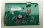
TPS57160EVM User's Guide
1
Introduction
1.1
Background
The TPS57160EVM evaluation module (EVM) is optimized to meet the Class 5 level of the CISPR25 EMC
Standard for automotive components. See the emissions report, SLVA629. As listed in Table 1, the EVM
requires an input voltage between 9 V and 16 V and provides an output voltage of 5 V at 1 A. The layout
has been designed to reduce emissions to levels deemed acceptable by the aforementioned standard.
The EVM features the TPS57160-Q1 step-down DC-DC converter which is a wide input voltage (3.5 V to
60 V) 1.5-A capable power device.
Along with the EMC optimization, this evaluation module also demonstrates the small printed-circuit-board
(PCB) areas that can be achieved when designing with the TPS57160-Q1 regulator. The switching
frequency is externally set at a nominal 2 MHz. The compensation components are external to the
integrated circuit (IC) and have been selected to optimize the transient performance of the device. An
external divider allows for an adjustable output voltage. Additionally, the TPS57160-Q1 device provides
adjustable slow start and undervoltage lockout through a resistor divider on the EN pin.
Table 1. Input and Output Summary
1.2
EVM
INPUT VOLTAGE RANGE
OUTPUT RANGE
TPS57160EVM
VIN = 9 V to 16 V
5 V at currents up to 1 A
Performance Specification Summary
Table 2 lists a summary of the TPS57160EVM performance specifications. Specifications are given for an
input voltage of VI = 12 V and an output voltage of VO = 5 V, unless otherwise specified. The
TPS57160EVM is designed and tested for VI = 9 V to 16 V. The ambient temperature is 25°C for all
measurements, unless otherwise noted.
Table 2. TPS57160EVM Performance Specification Summary
SPECIFICATION
TEST CONDITION
VIN operating voltage range
MIN
TYP
MAX
9
12
16
UNIT
V
VIN start voltage
6.45
V
VIN stop voltage
5.41
V
5
V
Output voltage set point
Output current range
VI = 9 V to 16 V
Output ripple voltage
IO = 1 A
Operating frequency
SLVUA80 – June 2014
Submit Documentation Feedback
0
1
A
10
mVPP
2000
kHz
TPS57160EVM User's Guide
Copyright © 2014, Texas Instruments Incorporated
1
�Introduction
1.3
www.ti.com
Modifications
This evaluation module is designed to provide access to the features of the TPS57160-Q1 device. Some
modifications can be made to the module.
1.3.1
Output Voltage Set Point
The voltage dividers R7 and R8 are used to set the output voltage. To change the output voltage of the
EVM, change the value of the resistor, R8. Changing the value of R8 can change the output voltage
above Vsense which is 0.8 V. Use Equation 1 to calculate the value of R8 for a specific output voltage.
R7
R8 =
VO
-1
V(VSENSE)
(1)
1.3.2
Slow-Start Time
The slow-start time can be adjusted by changing the value of C5. Use Equation 2 to calculate the required
value of C5 for a desired slow-start time.
T(SS) (ms) ´ I(SS) (µA)
C5 =
Vref (V) ´ 0.8
where
•
•
I(SS) is 2 µA
C5 is set to 0.015 µF on the EVM for a default slow-start time of 7.82 ms.
(2)
NOTE: The slow-start capacitor should remain lower than 0.47 µF and higher than 0.47 nF.
1.3.3
Adjustable Undervoltage Lockout
The undervoltage lockout (UVLO) can be adjusted externally using R3 and R4. The EVM is set for a start
voltage of 6.45 V and a stop voltage of 5.41 V using R3 = 348 kΩ and R4 = 78.7 kΩ. Use Equation 3 and
Equation 4 along with notes included in the TPS57160-Q1 datasheet (SLVSAP1) to calculate required
resistor values for different start and stop voltages.
V(start) - V(stop)
R3 =
2.9 ´ 10-6 A
(3)
1.25 V
R4 =
V(start) - V(stop)
+ 0.9 ´ 10-6 A
R3
(4)
2
TPS57160EVM User's Guide
SLVUA80 – June 2014
Submit Documentation Feedback
Copyright © 2014, Texas Instruments Incorporated
�Test Setup and Results
www.ti.com
2
Test Setup and Results
This section describes how to properly connect, set up, and use the TPS57160EVM evaluation module.
The section also includes the measured output voltage ripple of the EVM.
2.1
Input/Output Connections
The TPS57160EVM is provided with input connectors, output connectors, and test points as shown in
Table 3. A power supply capable of supplying 1 A must be connected to J1 through a pair of 20 AWG
(0.52 mm2 ) or larger wires. The load must be connected to J2 through a pair of 20 AWG (0.52 mm2 ) or
larger wires. The maximum load-current capability must be at least 1 A to use the full capability of this
EVM. Wire lengths must be minimized to reduce losses in the wires.
Table 3. EVM Connectors and Test Points
Reference Designator
Function
J1
VI (see Table 1 for VI range)
J2
VO, 5 V at 1 A maximum
TP1
TP2
TP3
GND Test Points
TP4
2.2
Output Voltage Ripple
Figure 1 shows the TPS57160EVM output voltage ripple. The output current is the rated full load current
of 1 A and VI = 12 V. The ripple voltage is measured directly across the output capacitor.
Figure 1. TPS57160EVM Output Ripple
SLVUA80 – June 2014
Submit Documentation Feedback
TPS57160EVM User's Guide
Copyright © 2014, Texas Instruments Incorporated
3
�Board Layout
3
www.ti.com
Board Layout
This section provides a description of the TPS57160EVM board layout and includes the layer figures.
3.1
Layout
Figure 2, Figure 3, Figure 4, Figure 5, Figure 5, and Figure 7 show the board layout for the
TPS57160EVM.
4
Figure 2. Top Layer
Figure 3. Inner Layer 1
Figure 4. Inner Layer 2
Figure 5. Bottom Layer
Figure 6. Top Overlay
Figure 7. Bottom Overlay
TPS57160EVM User's Guide
SLVUA80 – June 2014
Submit Documentation Feedback
Copyright © 2014, Texas Instruments Incorporated
�Schematic and Bill of Materials
www.ti.com
4
Schematic and Bill of Materials
4.1
Schematic
Figure 8 shows the schematic of the TPS57160EVM.
VIN_BUCK
L1
1.5µH
VOUT
PH1
U1
TPS54160DGQ
2
1
C1
4.7uF
C4
4.7uF
R3
348k
2
EN
3
J1
4
EN
9 to 16 Volts
R4
78.7k
C2
220uF
PH
EN
BOOT
VSENSE
SS/TR
PWRGD
5
+
VIN
RT/CLK
8
COMP
TP
GND
5V, 1A
L2
10
R1
1
7
FB
0
J2
C6
.1uF
6
R7
10.0k
11
9
D1
MBRA140LT3
C12
1.5nF
R6
20.5k
R5
53.6k
R9
10.0k
R2
10
C3
4.7uF
C5
.015uF
1
2
4.7µH
C9
10uF
FB
R8
1.87k
C8
39pF
C7
1200pF
GND
2MHz
VIN_BUCK
TP1
C10
.015uF
TP2
TP3
TP4
C11
.015uF
GND
GND
Figure 8. TPS57160EVM Schematic
SLVUA80 – June 2014
Submit Documentation Feedback
TPS57160EVM User's Guide
Copyright © 2014, Texas Instruments Incorporated
5
�Schematic and Bill of Materials
4.2
www.ti.com
Bill of Materials
Table 4 lists the bill of materials for the TPS57160EVM
Table 4. TPS57160EVM Bill of Materials
DESIGNATOR
QTY.
PCB
1
VALUE
DESCRIPTION
PACKAGE REFERENCE
Printed Circuit Board
PART NUMBER
MANUFACTURER
HVL080
Any
C1
C3
3
4.7 µF
Capacitor, ceramic, 25-V, X7R, 10%
1206
C3216X7R1E475K
TDK
1
220 µF
Capacitor, aluminum, electrolytic, 25-V, 20%
0.315 inch
25ZL220M8X11.5
Rubycon
3
.015 µF
Capacitor, ceramic, 50-V, X7R, 10%
0603
C1608X7R1H153K
TDK
C6
1
0.1 µF
Capacitor, ceramic, 50-V, X7R, 10%
0603
C1608X7R1H104K
TDK
C7
1
1200 pF
Capacitor, ceramic, 50-V, C0G, 5%
0603
C1608COG1H122J
TDK
C8
1
39 pF
Capacitor, ceramic, 50-V, C0G, 5%
0603
C1608COG1H390J
TDK
C9
1
10 µF
Capacitor, ceramic, 16-V, X7R, 10%
1206
C3216X7R1C106K
TDK
C12
1
1.5 nF
Capacitor, ceramic, 50-V, X7R, 10%
0603
C1608X7R1H153K
TDK
D1
1
MBRA140LT3
Diode, Schottky, 1-A, 40-V
SMA
MBRA130LT3
Motorola
6
Fiducial mark. There is nothing to buy or mount.
Fiducial
N/A
N/A
2
Terminal block, 6-A, 3.5-mm pitch, 2-Pos, TH
7.0 × 8.2 × 6.5mm
ED555/2DS
On-Shore Technology
C4
C2
C5,
C10
C11
FID1
FID2
FID3
FID4
FID5
FID6
J1
J2
L1
1
1.5 µH
Inductor, SMT, 9-A, 15-mΩ
IHLP-2525CZ
IHLP2525CZER1R5M01
Vishay-Dale
L2
1
4.7 µH
Inductor, SMT, 4.5-A, 40-mΩ
IHLP-2525CZ
IHLP2525CZER4R7M01
Vishay-Dale
Thermal Transfer Printable Labels, 0.650" W x
0.200" H - 10,000 per roll
PCB Label 0.650"H ×
0.200"W
THT-14-423-10
Brady
LBL1
1
R1
1
0
RES, 0 -Ω, 5%, 0.063-W, 0402
0402
RC0402JR-070RL
Yageo America
R2
1
10
RES, 10 -Ω, 5%, 0.1-W, 0603
0603
CRCW060310R0JNEA
Vishay-Dale
R3
1
348 kΩ
RES, 348-kΩ, 1%, 0.1-W, 0603
0603
CRCW0603348KFKEA
Vishay-Dale
R4
1
78.7 kΩ
RES, 78.7-kΩ, 1%, 0.1-W, 0603
0603
CRCW060378K7FKEA
Vishay-Dale
R5
1
53.6 kΩ
RES, 53.6-kΩ, 1%, 0.1-W, 0603
0603
CRCW060353K6FKEA
Vishay-Dale
6
TPS57160EVM User's Guide
SLVUA80 – June 2014
Submit Documentation Feedback
Copyright © 2014, Texas Instruments Incorporated
�Schematic and Bill of Materials
www.ti.com
Table 4. TPS57160EVM Bill of Materials (continued)
DESIGNATOR
QTY.
VALUE
DESCRIPTION
PACKAGE REFERENCE
PART NUMBER
MANUFACTURER
R6
1
20.5 kΩ
RES, 20.5-kΩ, 1%, 0.1-W, 0603
0603
CRCW060320K5FKEA
Vishay-Dale
2
10 kΩ
RES, 10-kΩ, 1%, 0.1-W, 0603
0603
CRCW060310K0FKEA
Vishay-Dale
1
1.87 kΩ
RES, 1.87-kΩ, 1%, 0.1-W, 0603
0603
CRCW06031K87FKEA
Vishay-Dale
4
5001
Test Point, Black, Thru Hole, Color Keyed
0.100 × 0.100 inch
5001
Keystone
1
TPS57160QDG
Q
IC, DC-DC Converter, 60-V, 1.5-A
DGQ0010D
TPS57160QDGQ
Texas Instruments
R7
R9
R8
TP1
TP2
TP3
TP4
U1
SLVUA80 – June 2014
Submit Documentation Feedback
TPS57160EVM User's Guide
Copyright © 2014, Texas Instruments Incorporated
7
�IMPORTANT NOTICE
Texas Instruments Incorporated and its subsidiaries (TI) reserve the right to make corrections, enhancements, improvements and other
changes to its semiconductor products and services per JESD46, latest issue, and to discontinue any product or service per JESD48, latest
issue. Buyers should obtain the latest relevant information before placing orders and should verify that such information is current and
complete. All semiconductor products (also referred to herein as “components”) are sold subject to TI’s terms and conditions of sale
supplied at the time of order acknowledgment.
TI warrants performance of its components to the specifications applicable at the time of sale, in accordance with the warranty in TI’s terms
and conditions of sale of semiconductor products. Testing and other quality control techniques are used to the extent TI deems necessary
to support this warranty. Except where mandated by applicable law, testing of all parameters of each component is not necessarily
performed.
TI assumes no liability for applications assistance or the design of Buyers’ products. Buyers are responsible for their products and
applications using TI components. To minimize the risks associated with Buyers’ products and applications, Buyers should provide
adequate design and operating safeguards.
TI does not warrant or represent that any license, either express or implied, is granted under any patent right, copyright, mask work right, or
other intellectual property right relating to any combination, machine, or process in which TI components or services are used. Information
published by TI regarding third-party products or services does not constitute a license to use such products or services or a warranty or
endorsement thereof. Use of such information may require a license from a third party under the patents or other intellectual property of the
third party, or a license from TI under the patents or other intellectual property of TI.
Reproduction of significant portions of TI information in TI data books or data sheets is permissible only if reproduction is without alteration
and is accompanied by all associated warranties, conditions, limitations, and notices. TI is not responsible or liable for such altered
documentation. Information of third parties may be subject to additional restrictions.
Resale of TI components or services with statements different from or beyond the parameters stated by TI for that component or service
voids all express and any implied warranties for the associated TI component or service and is an unfair and deceptive business practice.
TI is not responsible or liable for any such statements.
Buyer acknowledges and agrees that it is solely responsible for compliance with all legal, regulatory and safety-related requirements
concerning its products, and any use of TI components in its applications, notwithstanding any applications-related information or support
that may be provided by TI. Buyer represents and agrees that it has all the necessary expertise to create and implement safeguards which
anticipate dangerous consequences of failures, monitor failures and their consequences, lessen the likelihood of failures that might cause
harm and take appropriate remedial actions. Buyer will fully indemnify TI and its representatives against any damages arising out of the use
of any TI components in safety-critical applications.
In some cases, TI components may be promoted specifically to facilitate safety-related applications. With such components, TI’s goal is to
help enable customers to design and create their own end-product solutions that meet applicable functional safety standards and
requirements. Nonetheless, such components are subject to these terms.
No TI components are authorized for use in FDA Class III (or similar life-critical medical equipment) unless authorized officers of the parties
have executed a special agreement specifically governing such use.
Only those TI components which TI has specifically designated as military grade or “enhanced plastic” are designed and intended for use in
military/aerospace applications or environments. Buyer acknowledges and agrees that any military or aerospace use of TI components
which have not been so designated is solely at the Buyer's risk, and that Buyer is solely responsible for compliance with all legal and
regulatory requirements in connection with such use.
TI has specifically designated certain components as meeting ISO/TS16949 requirements, mainly for automotive use. In any case of use of
non-designated products, TI will not be responsible for any failure to meet ISO/TS16949.
Products
Applications
Audio
www.ti.com/audio
Automotive and Transportation
www.ti.com/automotive
Amplifiers
amplifier.ti.com
Communications and Telecom
www.ti.com/communications
Data Converters
dataconverter.ti.com
Computers and Peripherals
www.ti.com/computers
DLP® Products
www.dlp.com
Consumer Electronics
www.ti.com/consumer-apps
DSP
dsp.ti.com
Energy and Lighting
www.ti.com/energy
Clocks and Timers
www.ti.com/clocks
Industrial
www.ti.com/industrial
Interface
interface.ti.com
Medical
www.ti.com/medical
Logic
logic.ti.com
Security
www.ti.com/security
Power Mgmt
power.ti.com
Space, Avionics and Defense
www.ti.com/space-avionics-defense
Microcontrollers
microcontroller.ti.com
Video and Imaging
www.ti.com/video
RFID
www.ti-rfid.com
OMAP Applications Processors
www.ti.com/omap
TI E2E Community
e2e.ti.com
Wireless Connectivity
www.ti.com/wirelessconnectivity
Mailing Address: Texas Instruments, Post Office Box 655303, Dallas, Texas 75265
Copyright © 2014, Texas Instruments Incorporated
�


 工商网监
湘ICP备2023018690号
工商网监
湘ICP备2023018690号
