Sample &
Buy
Product
Folder
Support &
Community
Tools &
Software
Technical
Documents
TPS61200, TPS61201, TPS61202
SLVS577E – MARCH 2007 – REVISED DECEMBER 2014
TPS6120x Low Input Voltage Synchronous Boost Converter
With 1.3-A Switches
1 Features
3 Description
•
The TPS6120x devices provide a power supply
solution for products powered by either a single-cell,
two-cell, or three-cell alkaline, NiCd or NiMH, or onecell Li-Ion or Li-polymer battery. It is also used in fuel
cell or solar cell powered devices where the capability
of handling low input voltages is essential. Possible
output currents depend on the input to output voltage
ratio. The devices provide output currents of up to
600 mA at a 5-V output, while using a single-cell LiIon or Li-Polymer battery and discharges it down to
2.6 V. The boost converter is based on a fixed
frequency, pulse-width-modulation (PWM) controller
using synchronous rectification to obtain maximum
efficiency. At low load currents, the converter enters
the Power Save mode to maintain a high efficiency
over a wide load current range. The Power Save
mode can be disabled, forcing the converter to
operate at a fixed switching frequency. The average
input current is limited to a maximum value of 1500
mA. The output voltage is programmed by an
external resistor divider, or is fixed internally on the
chip. The converter can be disabled to minimize
battery drain. During shutdown, the load is completely
disconnected from the battery. The device is
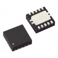
packaged in a 10-pin VSON package measuring 3
mm x 3 mm.
1
•
•
•
•
•
•
•
•
•
•
•
•
More than 90% Efficiency at
– 300 mA Output Current at 3.3 V
(VIN ≥ 2.4 V)
– 600 mA Output Current at 5 V (VIN ≥ 3 V)
Automatic Transition between Boost Mode and
Down Conversion Mode
Device Quiescent Current Less than 55 μA
Startup into Full Load at 0.5 V Input Voltage
Operating Input Voltage Range from
0.3 V to 5.5 V
Programmable Undervoltage Lockout Threshold
Output Short Circuit Protection Under all
Operating Conditions
Fixed and Adjustable Output Voltage Options from
1.8 V to 5.5 V
Power Save Mode for Improved Efficiency at Low
Output Power
Forced Fixed Frequency Operation Possible
Load Disconnect During Shutdown
Overtemperature Protection
Small 3 mm x 3 mm VSON-10 Package
Device Information(1)
2 Applications
•
•
•
•
•
•
•
PART NUMBER
All Single-Cell, Two-Cell and Three-Cell Alkaline,
NiCd or NiMH or Single-Cell Li Battery Powered
Products
Fuel Cell And Solar Cell Powered Products
Portable Audio Players
PDAs
Cellular Phones
Personal Medical Products
White LED Driver
TPS6120x
PACKAGE
VSON (10)
BODY SIZE (NOM)
3.00 mm × 3.00 mm
(1) For all available packages, see the orderable addendum at
the end of the datasheet.
4 Typical Application
L1
2.2 mH
VIN
0.3 V to 5.5 V
VIN
C1
L
VOUT
10 mF
EN
VAUX
PS
UVLO
FB
GND
PGND
C3
R1
C2
10 mF
0.1 mF
VOUT
1.8 V to 5.5 V
R2
TPS61200
1
An IMPORTANT NOTICE at the end of this data sheet addresses availability, warranty, changes, use in safety-critical applications,
intellectual property matters and other important disclaimers. PRODUCTION DATA.
�TPS61200, TPS61201, TPS61202
SLVS577E – MARCH 2007 – REVISED DECEMBER 2014
www.ti.com
Table of Contents
1
2
3
4
5
6
7
8
Features ..................................................................
Applications ...........................................................
Description .............................................................
Typical Application ................................................
Revision History.....................................................
Device Options.......................................................
Pin Configuration and Functions .........................
Specifications.........................................................
1
1
1
1
2
4
4
5
8.1
8.2
8.3
8.4
8.5
8.6
5
5
5
5
6
7
Absolute Maximum Ratings ......................................
ESD Ratings..............................................................
Recommended Operating Conditions.......................
Thermal Information ..................................................
Electrical Characteristics...........................................
Typical Characteristics ..............................................
9 Parameter Measurement Information ................ 10
10 Detailed Description ........................................... 11
10.1 Overview ............................................................... 11
10.2 Functional Block Diagram ..................................... 11
10.3 Feature Description............................................... 12
10.4 Device Functional Modes...................................... 13
11 Application and Implementation........................ 14
11.1 Application Information.......................................... 14
11.2 Typical Application ............................................... 14
11.3 System Examples ................................................. 19
12 Power Supply Recommendations ..................... 20
13 Layout................................................................... 21
13.1 Layout Guidelines ................................................. 21
13.2 Layout Example .................................................... 21
13.3 Thermal Considerations ........................................ 21
14 Device and Documentation Support ................. 22
14.1
14.2
14.3
14.4
Related Links ........................................................
Trademarks ...........................................................
Electrostatic Discharge Caution ............................
Glossary ................................................................
22
22
22
22
15 Mechanical, Packaging, and Orderable
Information ........................................................... 22
5 Revision History
NOTE: Page numbers for previous revisions may differ from page numbers in the current version.
Changes from Revision D (March 2013) to Revision E
•
Page
Added ESD Ratings table, Feature Description section, Device Functional Modes, Application and Implementation
section, Power Supply Recommendations section, Layout section, Device and Documentation Support section, and
Mechanical, Packaging, and Orderable Information section .................................................................................................. 1
Changes from Revision C (September 2012) to Revision D
•
Page
Changed the PS pin description From: Enable/disable Power Save mode (High = enabled, Low = disabled) To:
Enable/disable Power Save mode (High = disabled, Low = enabled) ................................................................................... 4
Changes from Revision B (FEBRUARY 2008) to Revision C
Page
•
Changed Feature From: Small 3 mm x 3 mm QFN-10 Package To: Small 3 mm x 3 mm SON-10 Package ...................... 1
•
Changed Application From: White LED's To: White LED Driver ............................................................................................ 1
•
Changed the Available Device Options Package type From: 10-PIN QFN To: 10-Pin SON ................................................. 4
•
Changed VSS to VIN in the Recommended Operating Conditions table ................................................................................. 5
•
Changed From: DISSIPATION RATINGS TABLE To: Thermal Information table ................................................................ 5
•
Changed the Parameters and Test Conditions in the Electrical Characteristics table .......................................................... 6
•
Updated Figure 1 through Figure 11 ...................................................................................................................................... 7
•
Added C3 to the List of Components ................................................................................................................................... 14
•
Added text to the Input Capacitor section "An R-C filter may be placed..." ......................................................................... 16
•
Added Figure 26, Figure 27, and Figure 28 ......................................................................................................................... 19
•
Added Figure 29 ................................................................................................................................................................... 21
2
Submit Documentation Feedback
Copyright © 2007–2014, Texas Instruments Incorporated
Product Folder Links: TPS61200 TPS61201 TPS61202
�TPS61200, TPS61201, TPS61202
www.ti.com
SLVS577E – MARCH 2007 – REVISED DECEMBER 2014
Changes from Revision A (JUNE 2007) to Revision B
•
Page
Added DSC package and tape and reel note to the Available Device Options. .................................................................... 4
Changes from Original (MARCH 2007) to Revision A
Page
•
Changed Features bullet From: 600 mA Output Current at 3.3 V (VIN ≥ 1.2 V) To: 300 mA Output Current at 3.3 V
(VIN ≥ 2.4 V)........................................................................................................................................................................... 1
•
Changed Figure 6 label From: Power Save Disabled To: Power Save Enabled .................................................................. 7
•
Changed Figure 7 label From: Power Save Enabled To: Power Save Disabled .................................................................. 8
Copyright © 2007–2014, Texas Instruments Incorporated
Product Folder Links: TPS61200 TPS61201 TPS61202
Submit Documentation Feedback
3
�TPS61200, TPS61201, TPS61202
SLVS577E – MARCH 2007 – REVISED DECEMBER 2014
www.ti.com
6 Device Options
TA
OUTPUT VOLTAGE (1)
PART NUMBER (2)
Adjustable
TPS61200DRC
3.3 V
TPS61201DRC
5V
TPS61202DRC
5V
TPS61202DSC
–40°C to 85°C
(1)
(2)
Contact the factory to check availability of other fixed output voltage versions.
The DRC and the DSC package are available taped and reeled. Add R suffix to device type (e.g., TPS61200DRCR or TPS61202DSCR)
to order quantities of 3000 devices per reel. It is also available in minireels. Add a T suffix to the device type (i.e. TPS61200DRCT or
TPS61202DSCT) to order quantities of 250 devices per reel.
7 Pin Configuration and Functions
DSC and DRC Package
10 Pins
Top View
VAUX
VOUT
L
PGND
VIN
1
2
3
10
Exposed
Thermal
Pad
9
8
4
7
5
6
FB
GND
PS
UVLO
EN
Pin Functions
PIN
NAME
NO.
I/O
DESCRIPTION
EN
6
I
Exposed
thermal pad
—
—
FB
10
I
GND
9
—
Control / logic ground
PGND
4
—
Power ground
PS
8
I
Enable/disable Power Save mode (High = disabled, Low = enabled). Do not leave floating.
L
3
I
Connection for Inductor
UVLO
7
I
Undervoltage lockout comparator input. Must be connected to VAUX if not used
VAUX
1
I/O
VIN
5
I
Boost converter input voltage
VOUT
2
O
Boost converter output
4
Enable input (High = enabled, Low = disabled). Do not leave floating.
Must be soldered to achieve appropriate power dissipation and mechanical reliability. Should be
connected to PGND.
Voltage feedback of adjustable versions, must be connected to VOUT at fixed output voltage versions
Supply voltage for control stage
Submit Documentation Feedback
Copyright © 2007–2014, Texas Instruments Incorporated
Product Folder Links: TPS61200 TPS61201 TPS61202
�TPS61200, TPS61201, TPS61202
www.ti.com
SLVS577E – MARCH 2007 – REVISED DECEMBER 2014
8 Specifications
8.1 Absolute Maximum Ratings
over operating free-air temperature range (unless otherwise noted) (1)
MIN
MAX
UNIT
VIN
Input voltage range on VIN, L, VAUX, VOUT, PS, EN, FB, UVLO
–0.3
7
V
TJ
Operating junction temperature
–40
150
°C
Tstg
Storage temperature
–65
150
°C
(1)
Stresses beyond those listed under Absolute Maximum Ratings may cause permanent damage to the device. These are stress ratings
only, and functional operation of the device at these or any other conditions beyond those indicated under Recommended Operating
Conditions is not implied. Exposure to absolute-maximum-rated conditions for extended periods may affect device reliability.
8.2 ESD Ratings
VALUE
V(ESD)
(1)
(2)
(3)
Electrostatic discharge
Human-body model (HBM), per ANSI/ESDA/JEDEC JS-001 (1)
±4000
Charged-device model (CDM), per JEDEC specification JESD22C101 (2)
±1500
Machine Model (MM) (3)
±200
UNIT
V
JEDEC document JEP155 states that 500-V HBM allows safe manufacturing with a standard ESD control process. Manufacturing with
less than 500-V HBM is possible with the necessary precautions.
JEDEC document JEP157 states that 250-V CDM allows safe manufacturing with a standard ESD control process. Manufacturing with
less than 250-V CDM is possible with the necessary precautions.
ESD testing is performed according to the respective JESD22 JEDEC standard.
8.3 Recommended Operating Conditions
MIN
VIN
Input voltage at VIN
0.3
TA
Operating free air temperature range
TJ
Operating junction temperature range
NOM
MAX
UNIT
5.5
V
–40
85
°C
–40
125
°C
8.4 Thermal Information
TPS6120x
THERMAL METRIC (1)
DRC
DSC
10 PINS
10 PINS
RθJA
Junction-to-ambient thermal resistance
41.2
40.4
RθJC(top)
Junction-to-case (top) thermal resistance
62.8
37.8
RθJB
Junction-to-board thermal resistance
16.6
15.4
ψJT
Junction-to-top characterization parameter
1.2
0.3
ψJB
Junction-to-board characterization parameter
16.8
15.6
RθJC(bot)
Junction-to-case (bottom) thermal resistance
4.1
2.8
(1)
UNIT
°C/W
For more information about traditional and new thermal metrics, see the IC Package Thermal Metrics application report, SPRA953.
Copyright © 2007–2014, Texas Instruments Incorporated
Product Folder Links: TPS61200 TPS61201 TPS61202
Submit Documentation Feedback
5
�TPS61200, TPS61201, TPS61202
SLVS577E – MARCH 2007 – REVISED DECEMBER 2014
www.ti.com
8.5 Electrical Characteristics
over recommended junction temperature range and over recommended input voltage range (typical at an ambient
temperature range of 25°C) (unless otherwise noted)
PARAMETER
TEST CONDITIONS
MIN
TYP
MAX
UNIT
DC-DC STAGE
VIN
Input voltage range
VIN
Minimum input voltage at startup
0.3
VOUT
TPS61200 output voltage range
1.8
VFB
TPS61200 feedback voltage
495
VOUT
TPS61201 output voltage
VIN < VOUT, PS = High
VOUT
TPS61202 output voltage
VIN < VOUT, PS = High
f
Oscillator frequency
ILIM
average inductor current limit
VOUT = 3.3 V
RDS(on)
Rectifying switch on resistance
VOUT = 3.3 V
RDS(on)
Main switch on resistance
VOUT = 3.3 V
Line regulation
VIN < VOUT, PS = High
0.1%
0.5%
VIN < VOUT, PS = High
0.1%
0.5%
VIN
IQ
Quiescent current
VAUX
ISD
Shutdown current
ILKG
Input leakage current ( L)
VIN
V
505
mV
3.27
3.3
3.33
V
4.95
5.0
5.05
V
1650
kHz
1200
1350
1500
180
VEN = 0 V, VIN = 1.2 V, VL = 1.2 V
mA
mΩ
150
VEN = 0 V, VIN = 1.2 V
VAUX
V
500
IO = 0 mA, VEN = VIN = 1.2 V,
VOUT = 3.3 V, VAUX = 3.3 V
PS = Low
VOUT
V
0.5
5.5
1250
Load regulation
5.5
mΩ
1
2
μA
50
70
μA
4
6
μA
0.5
1.5
μA
1
2
μA
0.01
1
μA
5.5
V
0.1 × VIN
V
CONTROL STAGE
VAUX
Auxiliary Output Voltage
VIL
Low level input threshold voltage (EN)
VIN < 0.8 V
VIH
High level input threshold voltage (EN)
VIN < 0.8 V
VIL
Low level input threshold voltage (EN)
0.8 V ≤ VIN ≤ 1.5 V
VIH
High level input threshold voltage (EN)
0.8 V ≤ VIN ≤ 1.5 V
VIL
Low level input threshold voltage (EN)
VIN > 1.5 V
VIH
High level input threshold voltage (EN)
VIN > 1.5 V
VIL
Low level input threshold voltage (PS)
VIH
High level input threshold voltage (PS)
ILKG
Input leakage current (EN, PS)
EN, PS = GND or VIN
VUVLO
Undervoltage lockout threshold
Falling UVLO voltage
VUVLO
Undervoltage lockout threshold
Rising UVLO voltage
ILKG
Input leakage current (UVLO)
VUVLO = 0.5 V
VOVP
Overvoltage protection threshold
Thermal shutdown temperature
2.4
0.9 × VIN
0.8 × VIN
1.2
Submit Documentation Feedback
V
V
0.4
V
0.01
0.1
μA
235
250
265
mV
330
350
370
mV
0.3
μA
1.2
V
5.5
Rising temperature
V
V
0.4
Thermal shutdown temperature
hysteresis
6
V
0.2 × VIN
7
V
140
°C
20
°C
Copyright © 2007–2014, Texas Instruments Incorporated
Product Folder Links: TPS61200 TPS61201 TPS61202
�TPS61200, TPS61201, TPS61202
www.ti.com
SLVS577E – MARCH 2007 – REVISED DECEMBER 2014
8.6 Typical Characteristics
Table 1. Table of Graphs
FIGURE
Maximum output current
Efficiency
Output voltage
vs Input voltage
Figure 1
vs Output current (TPS61200), Power Save Enabled
Figure 2
vs Output current (TPS61200), Power Save Disabled
Figure 3
vs Output current (TPS61201), Power Save Enabled
Figure 4
vs Output current (TPS61201), Power Save Disabled
Figure 5
vs Output current (TPS61202), Power Save Enabled
Figure 6
vs Output current (TPS61202), Power Save Disabled
Figure 7
vs Input voltage (TPS61201), Power Save Enabled
Figure 8
vs Input voltage (TPS61201), Power Save Disabled
Figure 9
vs Input voltage (TPS61202), Power Save Enabled
Figure 10
vs Input voltage (TPS61202), Power Save Disabled
Figure 11
vs Output current (TPS61201)
Figure 12
vs Output current (TPS61202)
Figure 13
100
1600
TPS61201
VO = 3.3 V
TPS61200
VO = 1.8 V,
Power Save Enabled
90
80
1200
TPS61200
VO = 1.8 V
1000
800
TPS61202
VO = 5 V
600
VI = 1.8 V
70
Efficiency - %
Maximum Output Current - mA
1400
60
50
40
VI = 0.9 V
30
400
20
200
10
0
0.10
0
0.2 0.6 1 1.4 1.8 2.2 2.6 3 3.4 3.8 4.2 4.6 5 5.4
VI - Input Voltage - V
100
100
VI = 1.8 V
90
80
80
70
70
Efficiency - %
Efficiency - %
TPS61200
VO = 1.8 V,
Power Save Disabled
60
50
40
VI = 0.9 V
20
10
10
Figure 3. Efficiency vs Output Current
VI = 1.8 V
VI = 0.9 V
40
20
1000
VI = 2.4 V
50
30
1
10
100
IO - Output Current - mA
TPS61201
VO = 3.3 V,
Power Save Enabled
60
30
0
0.10
1000
Figure 2. Efficiency vs Output Current
Figure 1. Maximum Output Current vs Input Voltage
90
1
10
100
IO - Output Current - mA
0
0.10
1
10
100
IO - Output Current - mA
1000
Figure 4. Efficiency vs Output Current
Copyright © 2007–2014, Texas Instruments Incorporated
Product Folder Links: TPS61200 TPS61201 TPS61202
Submit Documentation Feedback
7
�TPS61200, TPS61201, TPS61202
SLVS577E – MARCH 2007 – REVISED DECEMBER 2014
www.ti.com
100
100
TPS61201
VO = 3.3 V,
Power Save Disabled
90
90
80
80
VI = 2.4 V
70
Efficiency - %
70
Efficiency - %
VI = 3.6 V
VI = 2.4 V
VI = 1.8 V
60
50
VI = 0.9 V
40
50
30
20
20
10
10
1
10
100
IO - Output Current - mA
VI = 0.9 V
40
30
0
0.10
VI = 1.8 V
60
TPS61202
VO = 5 V,
Power Save Enabled
0
0.10
1000
100
100
VI = 3.6 V
TPS61202
VO = 5 V,
Power Save Disabled
IO = 100 mA
80
VI = 2.4 V
70
VI = 1.8 V
60
Efficiency - %
Efficiency - %
70
VI = 0.9 V
50
40
60
50
30
20
20
10
10
1
1k
10
100
IO - Output Current - mA
0
10k
IO = 10 mA
40
30
0
0.10
TPS61201
VO = 3.3 V,
Power Save Enabled
0
Figure 7. Efficiency vs Output Current
1
1.5
2 2.5 3 3.5 4
VI - Input Voltage - V
4.5
5 5.5
Figure 8. Efficiency vs Input Voltage
IO = 500 mA
IO = 1000 mA
IO = 500 mA
90
90
80
80
70
70
Efficiency - %
Efficiency - %
0.5
100
100
60
50
IO = 10 mA
IO = 100 mA
40
IO = 100 mA
IO = 1000 mA
60
50
IO = 10 mA
40
30
30
TPS61201
VO = 3.3 V,
Power Save Disabled
20
10
0
0.5
1
1.5
2 2.5 3 3.5 4
VI - Input Voltage - V
4.5
5 5.5
Figure 9. Efficiency vs Input Voltage
8
IO = 1000 mA
IO = 500 mA
90
80
0
1000
Figure 6. Efficiency vs Output Current
Figure 5. Efficiency vs Output Current
90
1
10
100
IO - Output Current - mA
Submit Documentation Feedback
20
TPS61202
VO = 5 V,
Power Save Enabled
10
0
0
0.5
1
1.5
2 2.5 3 3.5 4
VI - Input Voltage - V
4.5
5 5.5
Figure 10. Efficiency vs Input Voltage
Copyright © 2007–2014, Texas Instruments Incorporated
Product Folder Links: TPS61200 TPS61201 TPS61202
�TPS61200, TPS61201, TPS61202
www.ti.com
SLVS577E – MARCH 2007 – REVISED DECEMBER 2014
100
3.33
VI = 2.4 V
90
80
IO = 500 mA
Efficiency - %
IO = 1000 mA
VO - Output Voltage - V
IO = 100 mA
70
60
50
IO = 10 mA
40
30
TPS61202
VO = 5 V,
Power Save Disabled
20
10
0
0
0.5
1
1.5
2 2.5 3 3.5 4
VI - Input Voltage - V
4.5
TPS61201
VO = 3.3 V,
Power Save Disabled
3.27
1
5 5.5
10
100
IO - Output Current - mA
1000
Figure 12. Output Voltage vs Output Current
Figure 11. Efficiency vs Input Voltage
5.05
3.30
TPS61202
VO = 5 V,
Power Save Disabled
VO - Output Voltage - V
VI = 2.4 V
5
4.95
1
10
100
IO - Output Current - mA
1000
Figure 13. Output Voltage vs Output Current
Copyright © 2007–2014, Texas Instruments Incorporated
Product Folder Links: TPS61200 TPS61201 TPS61202
Submit Documentation Feedback
9
�TPS61200, TPS61201, TPS61202
SLVS577E – MARCH 2007 – REVISED DECEMBER 2014
www.ti.com
9 Parameter Measurement Information
L1
VIN
VIN
C1
L
VOUT
VOUT
EN
VAUX
PS
R1
C2
C3
UVLO
FB
GND
PGND
R2
TPS61200
Figure 14. Parameter Measurement Schematic
10
Submit Documentation Feedback
Copyright © 2007–2014, Texas Instruments Incorporated
Product Folder Links: TPS61200 TPS61201 TPS61202
�TPS61200, TPS61201, TPS61202
www.ti.com
SLVS577E – MARCH 2007 – REVISED DECEMBER 2014
10 Detailed Description
10.1 Overview
The TPS6120x is a low input voltage synchronous boost converter family. The devices support 0.3-V to 5.5-V
input voltage range, so can provide power supply solutions for products powered by either a single-cell, two-cell,
or three-cell alkaline, NiCd or NiMH, or one-cell Li-Ion or Li-polymer battery. It is also used in fuel cell or solar cell
powered devices where the capability of handling low input voltages is essential. The devices provide output
currents of up to 600 mA at a 5-V output, while using a single-cell Li-Ion or Li-Polymer battery and discharges it
down to 2.6 V. The boost converter is based on a fixed frequency, pulse-width-modulation (PWM) controller
using synchronous rectification to obtain maximum efficiency. At low load currents, the converter enters the
Power Save mode to maintain a high efficiency over a wide load current range. The Power Save mode can be
disabled, forcing the converter to operate at a fixed switching frequency. The average input current is limited to a
maximum value of 1500 mA. The output voltage is programmed by an external resistor divider, or is fixed
internally on the chip. The converter can be disabled to minimize battery drain. During shutdown, the load is
completely disconnected from the battery.
10.2 Functional Block Diagram
L
VOUT
VAUX
VCC
Control
Current
Sensor
VOUT
PGND
VIN
VCC
Gate
Control
FB
Modulator
VFB
PS
Oscillator
EN
Device
Control
UVLO
Thermal
Shutdown
GND
PGND
PGND
Copyright © 2007–2014, Texas Instruments Incorporated
Product Folder Links: TPS61200 TPS61201 TPS61202
Submit Documentation Feedback
11
�TPS61200, TPS61201, TPS61202
SLVS577E – MARCH 2007 – REVISED DECEMBER 2014
www.ti.com
10.3 Feature Description
10.3.1 Controller Circuit
The controlling circuit of the device is based on an average current mode topology. The average inductor current
is regulated by a fast current regulator loop which is controlled by a voltage control loop. The controller also uses
input and output voltage feedforward. Changes of input and output voltage are monitored and immediately
change the duty cycle in the modulator to achieve a fast response to those errors. The voltage error amplifier
gets its feedback input from the FB pin. For adjustable output voltage devices, a resistive voltage divider must be
connected to that pin. For fixed output voltage devices, FB must be connected to the output voltage to directly
sense the voltage. Fixed output voltage versions use a trimmed internal resistive divider. The feedback voltage is
compared with the internal reference voltage to generate a stable and accurate output voltage.
The controller circuit also senses the average input current as well as the peak input current. Thus, the maximum
input power is controlled as well as the maximum peak current, to achieve a safe and stable operation under all
possible conditions. To protect the device from overheating, an internal temperature sensor is implemented.
10.3.1.1 Synchronous Operation
The device uses three internal N-channel MOSFETs to maintain synchronous power conversion at all possible
operating conditions. This enables the device to keep high efficiency over a wide input voltage and output power
range.
To avoid ground shift problems due to the high currents in the switches, two separate ground pins, GND and
PGND, are used. The reference for all control functions is the GND pin. The power switches are connected to
PGND. Both grounds must be connected on the PCB at only one point, ideally close to the GND pin. Due to the
3-switch topology, the load is always disconnected from the input during shutdown of the converter.
10.3.1.2 Down Regulation
A boost converter only regulates output voltages which are higher than the input voltage. This device operates
differently. For example, it is able to regulate 3 V at the output with two fresh alkaline cells at the input having a
total cell voltage of 3.2 V. Another example is powering white LEDs with a forward voltage of 3.6 V from a fully
charged Li-Ion cell with an output voltage of 4.2 V. To control these applications properly, a Down Conversion
mode is implemented.
If the input voltage reaches or exceeds the output voltage, the converter automatically changes to a Down
Conversion mode. In this mode, the control circuit changes the behavior of the two rectifying switches. While
continuing switching, it sets the voltage drop across the rectifying switches as high as needed to regulate the
output voltage. This means the power losses in the converter increase. This must be taken into account for
thermal consideration.
10.3.1.3 Device Enable
The device is put into operation when EN is set high. It is put into Shutdown mode when EN is set to low. In
Shutdown mode, the regulator stops switching, all internal control circuitry including the UVLO comparator is
switched off, and the load is disconnected from the input. Current does not flow from input to output or from
output to input. This also means that the output voltage can drop below the input voltage during shutdown.
10.3.1.4 Softstart and Short-Circuit Protection
During start-up of the converter, the duty cycle and the peak current are limited in order to avoid high peak
currents drawn from the battery. After being enabled, the device starts operating. At first, it keeps the main output
VOUT disconnected, and charges the capacitor at VAUX. Once the capacitor at VAUX is charged to about 2.5 V,
the device switches to normal operation. This means VOUT is turned on and the capacitor at VOUT is charged,
while the load connected to the device is supplied. To ramp up the output voltage in a controlled way, the
average current limit is set to 400 mA and rises proportional to the increase of the output voltage. At an output
voltage of about 1.2 V the current limit is at its nominal value. If the output voltage does not increase, the current
limit does not increase. There is no timer implemented. Thus the output voltage overshoot at startup, as well as
the inrush current, is kept at a minimum. The device ramps up the output voltage in a controlled manner even if a
large capacitor is connected at the output. When the output voltage does not increase above 1.2 V, the device
assumes a short-circuit at the output, and keeps the current limit low to protect itself and the application. When
there is a short at the output during operation, the current limit is decreased accordingly.
12
Submit Documentation Feedback
Copyright © 2007–2014, Texas Instruments Incorporated
Product Folder Links: TPS61200 TPS61201 TPS61202
�TPS61200, TPS61201, TPS61202
www.ti.com
SLVS577E – MARCH 2007 – REVISED DECEMBER 2014
Feature Description (continued)
The device can also start into a Prebias on the outputs.
10.3.1.5 Current Limit
The device current limit limits the average current in the inductor. In a boost connector, this is the input current. If
an excessive load requires an input current greater than the average current limit, the device limits the input
current by reducing the output power delivered. In this case, the output voltage decreases.
10.3.1.6 Undervoltage Lockout
An undervoltage lockout function prevents the main output at VOUT from being supplied if the voltage at the
UVLO pin drops below 0.25 V. When using a resistive divider at the voltage to be monitored, for example the
supply voltage, any threshold for the monitored voltage can be programmed. If in undervoltage lockout mode, the
device still maintains its supply voltage at VAUX, and it is not turned off until EN is programmed low. This
undervoltage lockout function is implemented in order to prevent the malfunctioning of the converter.
10.3.1.7 Thermal Shutdown
The device has a built-in temperature sensor which monitors the internal IC temperature. If the temperature
exceeds the programmed threshold (see electrical characteristics table), the device stops operating. As soon as
the IC temperature has decreased below the programmed threshold, it starts operating again. There is a built-in
hysteresis to avoid unstable operation at IC temperatures at the thermal shutdown threshold.
10.4 Device Functional Modes
10.4.1 Power Save Mode
The Power Save (PS) pin can be used to select different operation modes. To enable Power Save mode the PS
pin must be set low. Power Save mode is used to improve efficiency at light load. If Power Save mode is
enabled, the converter stops operating if the average inductor current decreases below about 300 mA and the
output voltage is at or above its nominal value. If the output voltage decreases below its nominal value, the
device ramps up the output voltage again by starting operation using a programmed average inductor current
higher than required by the current load condition. Operation can last for one or several pulses. The converter
stops operating once the conditions for stopping operation are met again.
The Power Save mode can be disabled by programming a high at the PS pin. In Down Conversion mode, Power
Save mode is always enabled and the device cannot be forced into fixed frequency operation at light loads. The
PS input supports standard logic thresholds.
10.4.2 Down Conversion Mode
If the input voltage reaches or exceeds the output voltage, the converter automatically changes to a Down
Conversion mode. In this mode, the control circuit changes the behavior of the two rectifying switches. While
continuing switching, it sets the voltage drop across the rectifying switches as high as needed to regulate the
output voltage. This means the power losses in the converter increase. This must be taken into account for
thermal consideration.
Copyright © 2007–2014, Texas Instruments Incorporated
Product Folder Links: TPS61200 TPS61201 TPS61202
Submit Documentation Feedback
13
�TPS61200, TPS61201, TPS61202
SLVS577E – MARCH 2007 – REVISED DECEMBER 2014
www.ti.com
11 Application and Implementation
NOTE
Information in the following applications sections is not part of the TI component
specification, and TI does not warrant its accuracy or completeness. TI’s customers are
responsible for determining suitability of components for their purposes. Customers should
validate and test their design implementation to confirm system functionality.
11.1 Application Information
The TPS6120x DC-DC converters are intended for systems powered by a single up to triple cell Alkaline, NiCd,
NiMH battery with a typical terminal voltage between 0.7 V and 5.5 V. They can also be used in systems
powered by one-cell Li-Ion or Li-Polymer with a typical voltage between 2.5 V and 4.2 V. Additionally, any other
voltage source like solar cells or fuel cells with a typical output voltage between 0.3 V and 5.5 V can power
systems where the TPS6120x is used.
11.2 Typical Application
L1
VIN
VIN
C1
L
VOUT
VOUT
EN
R3
VAUX
PS
R1
C2
C3
UVLO
FB
R4
GND
PGND
R2
TPS61200
Figure 15. Typical Application Circuit for Adjustable Output Voltage Option
11.2.1 Design Requirements
In this example, TPS61200 is used to design a 3.3-V power supply with 100-mA output current capability. The
TPS61200 can be powered by either a single-cell, two-cell, or three-cell alkaline, NiCd or NiMH, or one-cell Li-Ion
or Li-Polymer battery. In this example, the input voltage range is from 0.8 V to 1.65 V for single-cell alkaline
input.
11.2.2 Detailed Design Procedure
Table 2. List of Components
COMPONENT REFERENCE
MANUFACTURER
VALUE
C1
any
10 μF, X7R Ceramic
C2
any
2 x 10 μF, X7R Ceramic
C3
any
1 µF, X7R, Ceramic
Coilcraft
2.2 μH
L1
PART NUMBER
LPS3015-222ML
11.2.2.1 Programming the Output Voltage
Within the TPS6120X family, there are fixed and adjustable output voltage versions available. To properly
configure the fixed output voltage devices, the FB pin is used to sense the output voltage. This means that it
must be connected directly to VOUT. For the adjustable output voltage version, an external resistor divider is
used to adjust the output voltage. The resistor divider must be connected between VOUT, FB and GND. When
the output voltage is regulated properly, the typical value of the voltage at the FB pin is 500 mV. The maximum
recommended value for the output voltage is 5.5 V. The current through the resistive divider should be about 100
times greater than the current into the FB pin. The typical current into the FB pin is 0.01 μA, and the voltage
14
Submit Documentation Feedback
Copyright © 2007–2014, Texas Instruments Incorporated
Product Folder Links: TPS61200 TPS61201 TPS61202
�TPS61200, TPS61201, TPS61202
www.ti.com
SLVS577E – MARCH 2007 – REVISED DECEMBER 2014
across the resistor between FB and GND, R2, is typically 500 mV. Based on those two values, the
recommended value for R2 should be lower than 500 kΩ, in order to set the divider current at 1 μA or higher. It is
recommended to keep the value for this resistor in the range of 200 kΩ. The value of the resistor connected
between VOUT and FB, R1, depending on the needed output voltage (VOUT), can be calculated using
Equation 1:
æV
ö
R1 = R2 x ç OUT - 1÷
è VFB
ø
(1)
As an example, for an output voltage of 3.3 V, a 1-MΩ resistor should be chosen for R1 when a 180-kΩ is
selected for R2.
11.2.2.2 Programming the UVLO Threshold Voltage
The UVLO input can be used to shut down the main output if the supply voltage is getting too low. The internal
reference threshold is typically 250 mV. If the supply voltage should cause the shutdown when it is dropping
below 250 mV, VIN can be connected directly to the UVLO pin. If the shutdown should happen at higher voltages,
a resistor divider can be used. R3 and R4 in Figure 15 show an example of how to monitor the input voltage of
the circuit. The current through the resistive divider should be about 100 times greater than the current into the
UVLO pin. The typical current into the UVLO pin is 0.01 μA, and the voltage across R4 is equal to the UVLO
voltage threshold that is generated on-chip, which has a value of 250 mV. Therefore, the recommended value for
R4 is in the range of 250 kΩ. From this, the value of resistor R3, depending on the desired shutdown voltage
VINMIN, can be calculated using Equation 2.
æV
ö
R3 = R4 x çç INMIN - 1÷÷
è VUVLO
ø
(2)
11.2.2.3 Inductor Selection
To make sure that the TPS6120X devices can operate, an inductor must be connected between the VIN and L
pins. To estimate the minimum inductance value, Equation 3 can be used.
ms
LMIN = VIN x 0.5
A
(3)
In Equation 3, the minimum inductance, LMIN , for boost mode operation is calculated. VIN is the maximum input
voltage. The recommended inductor value range is between 1.5 μH and 4.7 μH. The minimum inductor value
should not be below 1.5 μH, even if Equation 3 yields something lower. Using 2.2 μH is recommended anyway
for getting best performance over the whole input and output voltage range.
With the chosen inductance value, the peak current for the inductor in steady state operation can be calculated
using Equation 4.
ILMAX =
VIN x (VOUT - VIN )
VOUT x IOUT
+
0.8 x VIN
2 x VOUT x f x L
(4)
This would be the critical value for the current rating for selecting the inductor. It also needs to be taken into
account that load transients and error conditions may cause higher inductor currents. The following inductor
series from different suppliers have been used with TPS6120x converters:
Table 3. List of Inductors
VENDOR
Coilcraft
INDUCTOR SERIES
LPS3015
LPS4012
Murata
LQH3NP
Tajo Yuden
NR3015
Wurth Elektronik
WE-TPC Typ S
Copyright © 2007–2014, Texas Instruments Incorporated
Product Folder Links: TPS61200 TPS61201 TPS61202
Submit Documentation Feedback
15
�TPS61200, TPS61201, TPS61202
SLVS577E – MARCH 2007 – REVISED DECEMBER 2014
www.ti.com
11.2.2.4 Capacitor Selection
11.2.2.4.1
Input Capacitor
At least a 4.7-μF input capacitor is recommended to improve transient behavior of the regulator and EMI
behavior of the total power supply circuit. An X5R or X7R ceramic capacitor placed as close as possible to the
VIN and PGND pins of the IC is recommended.
An R-C filter may be placed on the VIN pin to improve performance in applications with a noisy input source. A
100-Ω resistor and 0.1-µF capacitor are recommended in this case. This filter is not required operation.
11.2.2.4.2
Output Capacitor
For the output capacitor, it is recommended to use small X5R or X7R ceramic capacitors placed as close as
possible to the VOUT and PGND pins of the IC. If, for any reason, the application requires the use of large
capacitors which can not be placed close to the IC, using a smaller ceramic capacitor in parallel to the large one
is required. This small capacitor should be placed as close as possible to the VOUT and PGND pins of the IC.
To get an estimate of the recommended minimum output capacitance, Equation 5 can be used.
mF
COUT = 5 x L x
mH
(5)
A capacitor with a value in the range of the calculated minimum should be used. This is required to maintain
control loop stability. There are no additional requirements regarding minimum ESR. There is also no upper limit
for the output capacitance value. Larger capacitors cause lower output voltage ripple as well as lower output
voltage drops during load transients.
11.2.2.4.3 Capacitor at VAUX
Between the VAUX pin and GND pin, a capacitor must be connected. This capacitor is used to maintain and filter
the control supply voltage, which is chosen from the highest of VIN, VOUT, and L. It is charged during startup
and before the main output VOUT is turned on. To ensure stable operation, using at least 0.1μF is
recommended. At output voltages below 2.5 V, the capacitance should be in the range of 1 μF. Since this
capacitor is also used as a snubber capacitor for the main switch, using a X5R or X7R ceramic capacitor with
low ESR is important.
11.2.3 Application Curves
FIGURE
Output Voltage TPS61201, Power Save Mode Disabled
Figure 16
Output Voltage TPS61202, Power Save Mode Disabled
Figure 17
Output Voltage TPS61201, Power Save Mode Enabled
Figure 18
Output Voltage TPS61202, Power Save Mode Enabled
Figure 19
TPS61201 Load Transient Response
Figure 20
TPS61202 Load Transient Response
Figure 21
TPS61201 Line Transient Response
Figure 22
TPS61202 Line Transient Response
Figure 23
TPS61201 Startup after Enable
Figure 24
TPS61202 Startup after Enable
Figure 25
16
Submit Documentation Feedback
Copyright © 2007–2014, Texas Instruments Incorporated
Product Folder Links: TPS61200 TPS61201 TPS61202
�TPS61200, TPS61201, TPS61202
SLVS577E – MARCH 2007 – REVISED DECEMBER 2014
Output Voltage
50 mV/div, AC
VI = 1.8 V, RL = 11W
TPS61202
VO = 5 V,
Power Save Disabled
VI = 1.8 V, RL = 17W
Inductor Current
200 mA/div, AC
TPS61201
VO = 3.3 V,
Power Save Disabled
Inductor Current
100 mA/div, AC
Output Voltage
20 mV/div, AC
www.ti.com
t - Time - 0.5 ms/div
t - Time - 1 ms/div
Figure 16. Output Voltage, Power Save Mode Disabled
Figure 17. Output Voltage, Power Save Mode Disabled
TPS61202
VO = 5 V,
Power Save Enabled
VI = 1.8 V, RL = 55 kW
Inductor Current
200 mA/div
Inductor Current
100 mA/div
Output Voltage
20 mV/div, AC
Output Voltage
20 mV/div, AC
VI = 1.8 V, RL = 33 kW
TPS61201
VO = 3.3 V,
Power Save Enabled
t - Time - 100 ms/div
Figure 18. Output Voltage in Power Save Mode
Figure 19. Output Voltage in Power Save Mode
Output Voltage
100 mV/div, AC
VI = 1.8 V, IL = 300 mA to 400 mA
TPS61202
VO = 5 V
VI = 1.8 V, IL = 150 mA to 250 mA
Output Current
100 mA/div, AC
TPS61201
VO = 3.3 V
Output Current
50 mA/div, AC
Output Voltage
50 mV/div, AC
t - Time - 2 ms/div
t - Time - 1 ms/div
t - Time - 1 ms/div
Figure 20. Load Transient Response
Figure 21. Load Transient Response
Copyright © 2007–2014, Texas Instruments Incorporated
Product Folder Links: TPS61200 TPS61201 TPS61202
Submit Documentation Feedback
17
�TPS61200, TPS61201, TPS61202
SLVS577E – MARCH 2007 – REVISED DECEMBER 2014
www.ti.com
VI = 1.8 V to 2.4 V, RL = 11W
Output Voltage
50 mV/div, AC
Output Voltage
20 mV/div, AC
Input Voltage
500 mV/div, AC
Input Voltage
500 mV/div, AC
VI = 3 V to 3.6 V, RL = 17W
TPS61202
VO = 5 V
TPS61201
VO = 3.3 V
t - Time - 2 ms/div
t - Time - 2 ms/div
Figure 22. Line Transient Response
Figure 23. Line Transient Response
Enable 5 V/div, DC
Enable 5 V/div, DC
Voltage at VAUX 2 V/div, DC
Voltage at VAUX 2 V/div, DC
Output Voltage 2 V/div, DC
Output Voltage 2 V/div, DC
Voltage at L 2 V/div, DC
Voltage at L 2 V/div, DC
Inductor Current 500 mA/div, DC
TPS61201
VO = 3.3 V
VI = 1.8 V, RL = 11W
t - Time - 100 ms/div
Figure 24. Start-Up After Enable
18
Submit Documentation Feedback
Inductor Current 500 mA/div, DC
TPS61201
VO = 3.3 V
VI = 1.8 V, RL = 17W
t - Time - 100 ms/div
Figure 25. Start-Up After Enable
Copyright © 2007–2014, Texas Instruments Incorporated
Product Folder Links: TPS61200 TPS61201 TPS61202
�TPS61200, TPS61201, TPS61202
www.ti.com
SLVS577E – MARCH 2007 – REVISED DECEMBER 2014
11.3 System Examples
Figure 26. WLED Driver Circuit (See SLVA364)
L1 4.7µH
Vcell = 0.3 - 0.5V
RefDes
C1
C2
C3
C4
C5
CFF
VCELL
EN
C1
UVLO
VAUX
PS
L
TPS61200
Solar Cell
VIN
GND
Value
>10 mF
>20 mF
1 mF
1 mF
10 nF
33 pF
VOUT
VOUT
R1
CFF
FB
VAUX
PGND
C2
R2
VAUX
Charge
storage
device
C3
R5
VAUX
C4
R3
R8
L1
RefDes
R1
R2
R3
R4
R5
R6
R7
R8
4.7 mH
Value
750 kW
200 kW
1 kW
1 MW
100 W
1 MW
100 kW
200 kW
R6
R4
VCELL
OPA379
TLV431
R7
MPP circuit
Power ground
C5
Reference ground
Figure 27. Solar Cell Circuit (See SLVA345)
Copyright © 2007–2014, Texas Instruments Incorporated
Product Folder Links: TPS61200 TPS61201 TPS61202
Submit Documentation Feedback
19
�TPS61200, TPS61201, TPS61202
SLVS577E – MARCH 2007 – REVISED DECEMBER 2014
www.ti.com
System Examples (continued)
L1
Inductor
2.2uH
3.3V
Vout
0.9V to 1.5V
R1
Vin
100
Battery
C1
10uF
TPS61200
Vaux
Vout
L
PGND
VIN
R2
0
C2
100nF
1
2
3
4
5
FB
10
GND
9
PS
8
UVLO
7
EN
6
C3
47uF
C4
10uF
R4
1K
TPS61200
R5
1K
R3
1K
Q1
MOSFET-N
GND
Figure 28. Reverse Battery Protection Circuit (See SLVA315)
12 Power Supply Recommendations
The power supply of TPS6120x DC-DC converters can be a single up to triple cell Alkaline, NiCd, NiMH battery
with a typical terminal voltage between 0.7 V and 5.5 V. The TPS6120x can also be powered by one-cell Li-Ion
or Li-Polymer with a typical voltage between 2.5 V and 4.2 V. Additionally, any other voltage source like solar
cells or fuel cells with a typical output voltage between 0.3 V and 5.5 V can also be the power supply.
The input supply should be well regulated with the rating of TPS6120x. If the input supply is located more than a
few inches from the device, additional bulk capacitance may be required in addition to the ceramic bypass
capacitors. An electrolytic or tantalum capacitor with a value of 47 µF is a typical choice.
20
Submit Documentation Feedback
Copyright © 2007–2014, Texas Instruments Incorporated
Product Folder Links: TPS61200 TPS61201 TPS61202
�TPS61200, TPS61201, TPS61202
www.ti.com
SLVS577E – MARCH 2007 – REVISED DECEMBER 2014
13 Layout
13.1 Layout Guidelines
As for all switching power supplies, the layout is an important step in the design, especially at high peak currents
and high switching frequencies. If the layout is not carefully done, the regulator could show stability problems as
well as EMI problems. Therefore, use wide and short traces for the main current path and for the power ground
tracks. The input and output capacitor, as well as the inductor should be placed as close as possible to the IC.
Use a common ground node for power ground and a different one for control ground to minimize the effects of
ground noise. Connect these ground nodes at any place close to one of the ground pins of the IC.
The feedback divider should be placed as close as possible to the control ground pin of the IC. To lay out the
control ground, it is recommended to use short traces as well, separated from the power ground traces. This
avoids ground shift problems, which can occur due to superimposition of power ground current and control
ground current. See Figure 29 for the recommended layout.
13.2 Layout Example
Figure 29. EVM Layout
13.3 Thermal Considerations
Implementation of integrated circuits in low-profile and fine-pitch surface-mount packages typically requires
special attention to power dissipation. Many system-dependent issues such as thermal coupling, airflow, added
heat sinks and convection surfaces, and the presence of other heat-generating components affect the powerdissipation limits of a given component.
Three basic approaches for enhancing thermal performance are listed below.
• Improving the power dissipation capability of the PCB design
• Improving the thermal coupling of the component to the PCB
• Introducing airflow in the system
The maximum recommended junction temperature (TJ) of the TPS6120x devices is 125°C. The thermal
resistance of the 10-pin SON 3 × 3 package (DRC) is RθJA = 41.2 °C/W, when the exposed thermal pad is
soldered. Specified regulator operation is assured to a maximum ambient temperature, TA, of 85°C. Therefore,
the maximum power dissipation is about 971 mW. More power can be dissipated if the maximum ambient
temperature of the application is lower.
TJ(MAX) - TA 125°C - 85°C
=
= 971mW
PD(MAX) =
RqJA
41.2°C / W
(6)
Copyright © 2007–2014, Texas Instruments Incorporated
Product Folder Links: TPS61200 TPS61201 TPS61202
Submit Documentation Feedback
21
�TPS61200, TPS61201, TPS61202
SLVS577E – MARCH 2007 – REVISED DECEMBER 2014
www.ti.com
14 Device and Documentation Support
14.1 Related Links
The table below lists quick access links. Categories include technical documents, support and community
resources, tools and software, and quick access to sample or buy.
Table 4. Related Links
PARTS
PRODUCT FOLDER
SAMPLE & BUY
TECHNICAL
DOCUMENTS
TOOLS &
SOFTWARE
SUPPORT &
COMMUNITY
TPS61200
Click here
Click here
Click here
Click here
Click here
TPS61201
Click here
Click here
Click here
Click here
Click here
TPS61202
Click here
Click here
Click here
Click here
Click here
14.2 Trademarks
All trademarks are the property of their respective owners.
14.3 Electrostatic Discharge Caution
These devices have limited built-in ESD protection. The leads should be shorted together or the device placed in conductive foam
during storage or handling to prevent electrostatic damage to the MOS gates.
14.4 Glossary
SLYZ022 — TI Glossary.
This glossary lists and explains terms, acronyms, and definitions.
15 Mechanical, Packaging, and Orderable Information
The following pages include mechanical, packaging, and orderable information. This information is the most
current data available for the designated devices. This data is subject to change without notice and revision of
this document. For browser-based versions of this data sheet, refer to the left-hand navigation.
22
Submit Documentation Feedback
Copyright © 2007–2014, Texas Instruments Incorporated
Product Folder Links: TPS61200 TPS61201 TPS61202
�PACKAGE OPTION ADDENDUM
www.ti.com
14-Oct-2022
PACKAGING INFORMATION
Orderable Device
Status
(1)
Package Type Package Pins Package
Drawing
Qty
Eco Plan
(2)
Lead finish/
Ball material
MSL Peak Temp
Op Temp (°C)
Device Marking
(3)
Samples
(4/5)
(6)
TPS61200DRCR
ACTIVE
VSON
DRC
10
3000
RoHS & Green
NIPDAU
Level-2-260C-1 YEAR
-40 to 85
BRR
Samples
TPS61200DRCRG4
ACTIVE
VSON
DRC
10
3000
RoHS & Green
NIPDAU
Level-2-260C-1 YEAR
-40 to 85
BRR
Samples
TPS61200DRCT
ACTIVE
VSON
DRC
10
250
RoHS & Green
NIPDAU
Level-2-260C-1 YEAR
-40 to 85
BRR
Samples
TPS61201DRCR
ACTIVE
VSON
DRC
10
3000
RoHS & Green
NIPDAU
Level-2-260C-1 YEAR
-40 to 85
BRS
Samples
TPS61201DRCT
ACTIVE
VSON
DRC
10
250
RoHS & Green
NIPDAU
Level-2-260C-1 YEAR
-40 to 85
BRS
Samples
TPS61202DRCR
ACTIVE
VSON
DRC
10
3000
RoHS & Green
NIPDAU
Level-2-260C-1 YEAR
-40 to 85
BRT
Samples
TPS61202DRCT
ACTIVE
VSON
DRC
10
250
RoHS & Green
NIPDAU
Level-2-260C-1 YEAR
-40 to 85
BRT
Samples
TPS61202DSCR
ACTIVE
WSON
DSC
10
3000
RoHS & Green
NIPDAU
Level-2-260C-1 YEAR
-40 to 85
CER
Samples
TPS61202DSCT
ACTIVE
WSON
DSC
10
250
RoHS & Green
NIPDAU
Level-2-260C-1 YEAR
-40 to 85
CER
Samples
(1)
The marketing status values are defined as follows:
ACTIVE: Product device recommended for new designs.
LIFEBUY: TI has announced that the device will be discontinued, and a lifetime-buy period is in effect.
NRND: Not recommended for new designs. Device is in production to support existing customers, but TI does not recommend using this part in a new design.
PREVIEW: Device has been announced but is not in production. Samples may or may not be available.
OBSOLETE: TI has discontinued the production of the device.
(2)
RoHS: TI defines "RoHS" to mean semiconductor products that are compliant with the current EU RoHS requirements for all 10 RoHS substances, including the requirement that RoHS substance
do not exceed 0.1% by weight in homogeneous materials. Where designed to be soldered at high temperatures, "RoHS" products are suitable for use in specified lead-free processes. TI may
reference these types of products as "Pb-Free".
RoHS Exempt: TI defines "RoHS Exempt" to mean products that contain lead but are compliant with EU RoHS pursuant to a specific EU RoHS exemption.
Green: TI defines "Green" to mean the content of Chlorine (Cl) and Bromine (Br) based flame retardants meet JS709B low halogen requirements of


 工商网监
湘ICP备2023018690号
工商网监
湘ICP备2023018690号
