www.ti.com
Table of Contents
User’s Guide
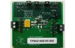
TPS6213x Buck Converter Evaluation Module User's
Guide
ABSTRACT
This user’s guide describes the characteristics, operation, and use of the Texas Instruments TPS62130,
TPS62140, and TPS62150 evaluation modules (EVM). These EVMs are designed to help the user easily
evaluate and test the operation and functionality of the TPS62130, TPS62140, and TPS62150. This user’s guide
includes setup instructions for the hardware, printed-circuit board layouts for the EVMs, a schematic diagram, a
bill of materials, and test results for the EVMs. After the release of the A-version devices in the summer of 2013,
these EVMs are assembled with the TPS62130A, TPS62140A, or TPS62150A.
Table of Contents
1 Introduction.............................................................................................................................................................................3
1.1 Background........................................................................................................................................................................ 3
1.2 Performance Specification................................................................................................................................................. 3
1.3 Modifications...................................................................................................................................................................... 3
2 Setup........................................................................................................................................................................................5
2.1 Input/Output Connector Descriptions................................................................................................................................. 5
2.2 Setup..................................................................................................................................................................................5
3 TPS621x0EVM-505 Test Results............................................................................................................................................6
4 Board Layout.........................................................................................................................................................................16
5 Schematic and Bill of Materials...........................................................................................................................................19
5.1 Schematic........................................................................................................................................................................ 19
5.2 Bill of Materials.................................................................................................................................................................20
6 Revision History................................................................................................................................................................... 20
List of Figures
Figure 1-1. Loop Response Measurement Modification.............................................................................................................. 4
Figure 3-1. Efficiency With 1-µH Inductor and FSW = LOW (high frequency).............................................................................6
Figure 3-2. Efficiency With 2.2-µH Inductor and FSW = LOW (high frequency)..........................................................................6
Figure 3-3. Efficiency With 2.2-µH Inductor and FSW = HIGH (low frequency).......................................................................... 7
Figure 3-4. Load Regulation With 2.2-µH Inductor and FSW = LOW (high frequency)...............................................................7
Figure 3-5. Line Regulation With 2.2-µH Inductor and FSW = LOW (high frequency) and Iout = 1 A.........................................8
Figure 3-6. Loop Response With 2.2-µH Inductor and FSW = LOW (high frequency) and VIN = 12 V and IOUT = 1 A............... 8
Figure 3-7. Input Voltage Ripple With 2.2-µH Inductor and FSW = LOW (high frequency) and Vin = 12 V and Iout = 1 A.........9
Figure 3-8. Output Voltage Ripple With 2.2-µH Inductor and FSW = LOW (high frequency) and Vin = 12 V and Iout = 1 A...... 9
Figure 3-9. Output Voltage Ripple With 2.2-µH Inductor and FSW = HIGH (low frequency) and Vin = 12 V and Iout = 1 A.....10
Figure 3-10. Load Transient Response With 1-µH Inductor and Vin = 12 V..............................................................................10
Figure 3-11. Load Transient Response With 2.2-µH Inductor and Vin = 12 V........................................................................... 11
Figure 3-12. Start-Up on EN with 1 A Load and Vin = 12 V.......................................................................................................11
Figure 3-13. Shutdown on EN with 1 A Load and Vin = 12 V.................................................................................................... 12
Figure 3-14. TPS62130 Prebias Start-Up and Shutdown on EN With 1-A Load and Vin = 12 V.............................................. 12
Figure 3-15. TPS62130A Prebias Start-Up and Shutdown on EN With 1-A Load and Vin = 12 V............................................ 13
Figure 3-16. Thermal Performance With 1-µH Inductor and Vin = 12 V and Iout = 3 A and FSW = LOW (high frequency)..... 14
Figure 3-17. Thermal Performance With 2.2-µH Inductor Vin = 12 V and Iout = 3 A and FSW = HIGH (low frequency)..........15
Figure 4-1. Assembly Layer.......................................................................................................................................................16
Figure 4-2. Top Layer Routing................................................................................................................................................... 16
Figure 4-3. Internal Layer-1 Routing..........................................................................................................................................17
Figure 4-4. Internal Layer-2 Routing..........................................................................................................................................17
Figure 4-5. Bottom Layer Routing..............................................................................................................................................18
SLVU437B – OCTOBER 2011 – REVISED JUNE 2021
Submit Document Feedback
TPS6213x Buck Converter Evaluation Module User's Guide
Copyright © 2021 Texas Instruments Incorporated
1
�Trademarks
www.ti.com
Figure 5-1. TPS621x0EVM-505 Schematic...............................................................................................................................19
List of Tables
Table 1-1. Performance Specification Summary..........................................................................................................................3
Table 5-1. TPS621x0EVM-505 Bill of Materials.........................................................................................................................20
Trademarks
All trademarks are the property of their respective owners.
2
TPS6213x Buck Converter Evaluation Module User's Guide
Copyright © 2021 Texas Instruments Incorporated
SLVU437B – OCTOBER 2011 – REVISED JUNE 2021
Submit Document Feedback
�www.ti.com
Introduction
1 Introduction
The TPS62130 is a 3-A, synchronous, step-down converter in a 3x3-mm, 16-pin QFN package. Both fixed and
adjustable output voltage units are available.
The TPS62140 is a 2-A, synchronous, step-down converter in a 3x3-mm, 16-pin QFN package. Both fixed and
adjustable output voltage units are available.
The TPS62150 is a 1-A, synchronous, step-down converter in a 3x3-mm, 16-pin QFN package. Both fixed and
adjustable output voltage units are available.
1.1 Background
The TPS62130EVM-505 (HPA505-001) uses the TPS62130A adjustable version and is set to a 3.3-V output.
The EVM operates with full-rated performance with an input voltage between 3.7 V and 17 V.
The TPS62140EVM-505 (HPA505-002) uses the TPS62140A adjustable version and is set to a 3.3-V output.
The EVM operates with full-rated performance with an input voltage between 3.7 V and 17 V.
The TPS62150EVM-505 (HPA505-003) uses the TPS62150A adjustable version and is set to a 3.3-V output.
The EVM operates with full-rated performance with an input voltage between 3.7 V and 17 V.
1.2 Performance Specification
Table 1-1 provides a summary of the TPS621x0EVM-505 performance specifications. All specifications are given
for an ambient temperature of 25°C.
Table 1-1. Performance Specification Summary
Specification
Test Conditions
Min
Input Voltage
Typ
Max
17
V
3.327
3.387
V
3.7
3.268
Unit
Output Voltage
PWM Mode of Operation
Output Current
TPS62130EVM-505
0
3000
mA
TPS62140EVM-505
0
2000
mA
TPS62150EVM-505
0
1000
mA
Peak Efficiency
TPS62130EVM-505, FSW = LOW (high frequency)
93.2%
Peak Efficiency
TPS62140EVM-505 and TPS62150EVM-505, FSW = HIGH (low
frequency)
95.0%
Soft-Start Time
1.65
ms
1.3 Modifications
The printed-circuit board (PCB) for this EVM is designed to accommodate both the fixed and adjustable voltage
versions of this integrated circuit (IC). Additional input and output capacitors can also be added, and the
soft-start time can be changed. Finally, the loop response of the IC can be measured.
1.3.1 Fixed Output Operation
U1 can be replaced with the fixed-voltage version of the IC for evaluation. For fixed-voltage version operation,
replace R2 with a 0-Ω resistor and remove R1.
1.3.2 Input and Output Capacitors
C2 is provided for an additional input capacitor. This capacitor is not required for proper operation but can be
used to reduce the input voltage ripple.
C7 is provided for an input capacitor on the AVIN pin. This capacitor is required and populated on the
TPS62130EVM-505. It may be added on the other EVM versions but is not required.
C4 is provided for an additional output capacitor. This capacitor is not required for proper operation but can
be used to reduce the output voltage ripple and to improve the load transient response. The total output
capacitance must remain within the recommended range in the data sheet for proper operation.
SLVU437B – OCTOBER 2011 – REVISED JUNE 2021
Submit Document Feedback
TPS6213x Buck Converter Evaluation Module User's Guide
Copyright © 2021 Texas Instruments Incorporated
3
�Introduction
www.ti.com
1.3.3 Soft-Start Time
C5 controls the soft-start time of the output voltage on the TPS621x0EVM-505. It can be changed for a shorter
or slower ramp up of Vout. Note that as the value of C5 is decreased, the inrush current increases.
1.3.4 Loop Response Measurement
The loop response of the TPS621x0EVM-505 can be measured with two simple changes to the circuitry. First,
install a 10-Ω resistor across the pads in the middle of the back of the PCB. The pads are spaced to allow
installation of 0805- or 0603-sized resistors. Second, cut the trace between the via on the output voltage and
the trace that connects to the VOS pin via. These changes are shown in Figure 1-1. With these changes, an
ac signal (10-mV, peak-to-peak amplitude recommended) can be injected into the control loop across the added
resistor.
Cut This Trace
Added Resistor
Figure 1-1. Loop Response Measurement Modification
4
TPS6213x Buck Converter Evaluation Module User's Guide
Copyright © 2021 Texas Instruments Incorporated
SLVU437B – OCTOBER 2011 – REVISED JUNE 2021
Submit Document Feedback
�www.ti.com
Setup
2 Setup
This section describes how to properly use the TPS621x0EVM-505.
2.1 Input/Output Connector Descriptions
J1 – VIN
Positive input connection from the input supply for the EVM. Use when the steady-state input current is less than 1
A. Otherwise, use J8.
J2 – S+/S–
Input voltage sense connections. Measure the input voltage at this point.
J3 – GND
Return connection from the input supply for the EVM. Use when the steady-state input current is less than 1 A.
Otherwise, use J8.
J4 – VOUT
Output voltage connection. Use when the steady-state output current is less than 1 A. Otherwise, use J9.
J5 – S+/S–
Output voltage sense connections. Measure the output voltage at this point.
J6 – GND
Output return connection. Use when the steady-state output current is less than 1 A. Otherwise, use J9.
J7 – PG/GND
The PG output appears on pin 1 of this header with a convenient ground on pin 2.
J8 – VIN/GND
Pin 1 is the positive input connection with pin 2, serving as the return connection. Use this terminal block if the
steady-state input current is greater than 1 A.
J9 – VOUT/GND
Pin 2 is the output voltage connection with pin 1, serving as the output return connection. Use this terminal block if
the steady-state output current is greater than 1 A.
J10 – SS/TR & GND
The SS/TR input appears on pin 1 of this header with a convenient ground on pin 2
JP1 – EN
EN pin input jumper. Place the supplied jumper across ON and EN to turn on the IC. Place the jumper across OFF
and EN to turn off the IC.
JP2 – DEF
DEF pin input jumper. Place the supplied jumper across HIGH and DEF to set the output voltage at 5% above
nominal. Place the jumper across LOW and DEF to set the output voltage at the nominal level.
JP3 – FSW
FSW pin input jumper. Place the supplied jumper across 1.25MHz and FSW to operate the IC at a reduced switching
frequency of nominally 1.25 MHz. Place the jumper across 2.5MHz and FSW to operate the IC at the full switching
frequency of nominally 2.5 MHz.
JP4 – PG Pullup
Voltage
PG pin pullup voltage jumper. Place the supplied jumper on JP4 to connect the PG pin pullup resistor to Vout.
Alternatively, the jumper can be removed and a different voltage can be supplied on pin 2 to pull up the PG pin to a
different level. This externally applied voltage must remain below 7 V.
2.2 Setup
To operate the EVM, set jumpers JP1 through JP4 to the desired positions per Section 2.1. Connect the input
supply to either J1 and J3 or J8, and connect the load to either J4 and J6 or J9.
SLVU437B – OCTOBER 2011 – REVISED JUNE 2021
Submit Document Feedback
TPS6213x Buck Converter Evaluation Module User's Guide
Copyright © 2021 Texas Instruments Incorporated
5
�TPS621x0EVM-505 Test Results
www.ti.com
3 TPS621x0EVM-505 Test Results
This section provides test results of the TPS621x0EVM-505.
100
VI = 9 V
90
VI = 12 V
VI = 15 V
VI = 5 V
Efficiency - %
80
VI = 17 V
70
60
50
40
0.0001
0.001
0.01
0.1
Load Current - A
1
10
Figure 3-1. Efficiency With 1-µH Inductor and FSW = LOW (high frequency)
100
VI = 15 V
90
VI = 12 V
VI = 9 V
Efficiency - %
80
VI = 5 V
70
VI = 17 V
60
50
40
0.0001
0.001
0.01
0.1
Load Current - A
1
10
Figure 3-2. Efficiency With 2.2-µH Inductor and FSW = LOW (high frequency)
6
TPS6213x Buck Converter Evaluation Module User's Guide
Copyright © 2021 Texas Instruments Incorporated
SLVU437B – OCTOBER 2011 – REVISED JUNE 2021
Submit Document Feedback
�www.ti.com
TPS621x0EVM-505 Test Results
100
VI = 9 V
90
VI = 12 V
VI = 15 V
VI = 5 V
Efficiency - %
80
VI = 17 V
70
60
50
40
0.0001
0.001
0.01
0.1
Load Current - A
1
10
Figure 3-3. Efficiency With 2.2-µH Inductor and FSW = HIGH (low frequency)
0.6
VI = 17 V
0.5
VI = 15 V
VI = 12 V
Load Regulation - %
0.4
VI = 9 V
0.3
0.2
0.1
VI = 5 V
0
-0.1
-0.2
0.0001
0.001
0.01
0.1
Load Current - A
1
10
Figure 3-4. Load Regulation With 2.2-µH Inductor and FSW = LOW (high frequency)
SLVU437B – OCTOBER 2011 – REVISED JUNE 2021
Submit Document Feedback
TPS6213x Buck Converter Evaluation Module User's Guide
Copyright © 2021 Texas Instruments Incorporated
7
�TPS621x0EVM-505 Test Results
www.ti.com
0.2
Line Regulation - %
0.15
0.1
0.05
0
-0.05
-0.1
3
5
7
9
11
VI - Input Voltage - V
13
15
17
60
180
50
150
40
120
30
90
20
60
10
30
0
0
Phase - deg
Gain - dB
Figure 3-5. Line Regulation With 2.2-µH Inductor and FSW = LOW (high frequency) and Iout = 1 A
-10
-30
-20
-60
-30
-90
-40
-120
-50
-150
-60
100
1k
10k
f - Frequency - Hz
100k
-180
1M
Figure 3-6. Loop Response With 2.2-µH Inductor and FSW = LOW (high frequency) and VIN = 12 V and
IOUT = 1 A
8
TPS6213x Buck Converter Evaluation Module User's Guide
Copyright © 2021 Texas Instruments Incorporated
SLVU437B – OCTOBER 2011 – REVISED JUNE 2021
Submit Document Feedback
�www.ti.com
TPS621x0EVM-505 Test Results
VIN (AC Coupled) 20 mV/div
Iind 0.5 A/div
SW 10 V/div
t - Time - 200 ns/div
Figure 3-7. Input Voltage Ripple With 2.2-µH Inductor and FSW = LOW (high frequency) and Vin = 12 V
and Iout = 1 A
VOUT (AC Coupled) 20 mV/div
Iind 0.5 A/div
SW 10 V/div
t - Time - 200 ns/div
Figure 3-8. Output Voltage Ripple With 2.2-µH Inductor and FSW = LOW (high frequency) and Vin = 12 V
and Iout = 1 A
SLVU437B – OCTOBER 2011 – REVISED JUNE 2021
Submit Document Feedback
TPS6213x Buck Converter Evaluation Module User's Guide
Copyright © 2021 Texas Instruments Incorporated
9
�TPS621x0EVM-505 Test Results
www.ti.com
VOUT (AC Coupled) 20 mV/div
Iind 0.5 A/div
SW 10 V/div
t - Time - 200 ns/div
Figure 3-9. Output Voltage Ripple With 2.2-µH Inductor and FSW = HIGH (low frequency) and Vin = 12 V
and Iout = 1 A
VOUT (AC Coupled) 20 mV/div
1 A to 2 A Load Step
ILoad 1 A/div
t - Time - 2 ms/div
Figure 3-10. Load Transient Response With 1-µH Inductor and Vin = 12 V
10
TPS6213x Buck Converter Evaluation Module User's Guide
Copyright © 2021 Texas Instruments Incorporated
SLVU437B – OCTOBER 2011 – REVISED JUNE 2021
Submit Document Feedback
�www.ti.com
TPS621x0EVM-505 Test Results
VOUT (AC Coupled) 20 mV/div
0.5 A to 1 A Load Step
ILoad 0.5 A/div
t - Time - 2 ms/div
Figure 3-11. Load Transient Response With 2.2-µH Inductor and Vin = 12 V
VIN 10 V/div
EN 10 V/div
VOUT 1 V/div
SS/TR 1 V/div
t - Time - 1 ms/div
Figure 3-12. Start-Up on EN with 1 A Load and Vin = 12 V
SLVU437B – OCTOBER 2011 – REVISED JUNE 2021
Submit Document Feedback
TPS6213x Buck Converter Evaluation Module User's Guide
Copyright © 2021 Texas Instruments Incorporated
11
�TPS621x0EVM-505 Test Results
www.ti.com
VIN 10 V/div
EN 10 V/div
VOUT 1 V/div
PG 1 V/div
t - Time - 100 ms/div
Figure 3-13. Shutdown on EN with 1 A Load and Vin = 12 V
VIN 10 V/div
EN 1 V/div
1.5 V Pre-bias
VOUT 1 V/div
PG 2 V/div
t - Time - 500 ms/div
Figure 3-14. TPS62130 Prebias Start-Up and Shutdown on EN With 1-A Load and Vin = 12 V
12
TPS6213x Buck Converter Evaluation Module User's Guide
Copyright © 2021 Texas Instruments Incorporated
SLVU437B – OCTOBER 2011 – REVISED JUNE 2021
Submit Document Feedback
�www.ti.com
TPS621x0EVM-505 Test Results
VIN 10 V/div
EN 1 V/div
1.5 V Pre-bias
VOUT 1 V/div
PG 2 V/div
t - Time - 500 ms/div
Figure 3-15. TPS62130A Prebias Start-Up and Shutdown on EN With 1-A Load and Vin = 12 V
SLVU437B – OCTOBER 2011 – REVISED JUNE 2021
Submit Document Feedback
TPS6213x Buck Converter Evaluation Module User's Guide
Copyright © 2021 Texas Instruments Incorporated
13
�TPS621x0EVM-505 Test Results
www.ti.com
Figure 3-16. Thermal Performance With 1-µH Inductor and Vin = 12 V and Iout = 3 A and FSW = LOW
(high frequency)
14
TPS6213x Buck Converter Evaluation Module User's Guide
Copyright © 2021 Texas Instruments Incorporated
SLVU437B – OCTOBER 2011 – REVISED JUNE 2021
Submit Document Feedback
�www.ti.com
TPS621x0EVM-505 Test Results
Figure 3-17. Thermal Performance With 2.2-µH Inductor Vin = 12 V and Iout = 3 A and FSW = HIGH (low
frequency)
SLVU437B – OCTOBER 2011 – REVISED JUNE 2021
Submit Document Feedback
TPS6213x Buck Converter Evaluation Module User's Guide
Copyright © 2021 Texas Instruments Incorporated
15
�Board Layout
www.ti.com
4 Board Layout
This section provides the TPS621x0EVM-505 board layout and illustrations.
Figure 4-1. Assembly Layer
Figure 4-2. Top Layer Routing
16
TPS6213x Buck Converter Evaluation Module User's Guide
Copyright © 2021 Texas Instruments Incorporated
SLVU437B – OCTOBER 2011 – REVISED JUNE 2021
Submit Document Feedback
�www.ti.com
Board Layout
Figure 4-3. Internal Layer-1 Routing
Figure 4-4. Internal Layer-2 Routing
SLVU437B – OCTOBER 2011 – REVISED JUNE 2021
Submit Document Feedback
TPS6213x Buck Converter Evaluation Module User's Guide
Copyright © 2021 Texas Instruments Incorporated
17
�Board Layout
www.ti.com
Figure 4-5. Bottom Layer Routing
18
TPS6213x Buck Converter Evaluation Module User's Guide
Copyright © 2021 Texas Instruments Incorporated
SLVU437B – OCTOBER 2011 – REVISED JUNE 2021
Submit Document Feedback
�www.ti.com
Schematic and Bill of Materials
5 Schematic and Bill of Materials
This section provides the TPS621x0EVM-505 schematic and bill of materials.
+
5.1 Schematic
Figure 5-1. TPS621x0EVM-505 Schematic
SLVU437B – OCTOBER 2011 – REVISED JUNE 2021
Submit Document Feedback
TPS6213x Buck Converter Evaluation Module User's Guide
Copyright © 2021 Texas Instruments Incorporated
19
�Schematic and Bill of Materials
www.ti.com
5.2 Bill of Materials
Table 5-1. TPS621x0EVM-505 Bill of Materials
Count
-001 -002
-003
RefDes
Value
Description
Size
Part Number
MFR
1
1
1
C1
10 µF
Capacitor, Ceramic, 25V, X5R, 20%
1210
Std
Std
1
1
1
C3
22 µF
Capacitor, Ceramic, 6.3V, X5R, 20%
0805
Std
Std
1
1
1
C5
3300 pF
Capacitor, Ceramic, 25V, X7R, 10%
0603
Std
Std
1
1
1
C6
68 µF
Capacitor, Tantalum, 35V, 68uF, ±20%
7361[V]
TPSV686M035R0150
AVX
1
0
0
C7
0.1 µF
Capacitor, Ceramic, 25V, X5R, 20%
0603
Std
Std
1
0
0
L1
1.0 µH
Inductor, Power, 5.1A, ±20%
0.165 x 0.165 inch
XFL4020-102ME
Coilcraft
0
1
1
L1
2.2 µH
Inductor, Power, 3.5A, ±20%
0.165 x 0.165 inch
XFL4020-222ME
Coilcraft
1
1
1
R1
1.21M
Resistor, Chip, 1/16W, 1%
0603
Std
Std
1
1
1
R2
383k
Resistor, Chip, 1/16W, 1%
0603
Std
Std
1
1
1
R3
100k
Resistor, Chip, 1/16W, 1%
0603
Std
Std
1
0
0
U1(1)
TPS62130ARGT
IC, 17V 3A Step-Down Converter in 3 mm x 3 mm QFN
Package
3 x 3 mm QFN
TPS62130ARGT
TI
0
1
0
U1(1)
TPS62140ARGT
IC, 17V 2A Step-Down Converter in 3 mm x 3 mm QFN
Package
3 x 3 mm QFN
TPS62140ARGT
TI
0
0
1
U1(1)
TPS62150ARGT
IC, 17V 1A Step-Down Converter in 3 mm x 3 mm QFN
Package
3 x 3 mm QFN
TPS62150ARGT
TI
(1)
EVMs made before August of 2013 use the non-A version of U1. The only difference between these devices is the operation of the PG
pin when the device is disabled, as shown in Figure 3-14 and Figure 3-15.
6 Revision History
NOTE: Page numbers for previous revisions may differ from page numbers in the current version.
Changes from Revision A (July 2013) to Revision B (June 2021)
Page
• Updated the numbering format for tables, figures, and cross-references throughout the document. ................3
• Updated user's guide title................................................................................................................................... 3
20
TPS6213x Buck Converter Evaluation Module User's Guide
Copyright © 2021 Texas Instruments Incorporated
SLVU437B – OCTOBER 2011 – REVISED JUNE 2021
Submit Document Feedback
�IMPORTANT NOTICE AND DISCLAIMER
TI PROVIDES TECHNICAL AND RELIABILITY DATA (INCLUDING DATA SHEETS), DESIGN RESOURCES (INCLUDING REFERENCE
DESIGNS), APPLICATION OR OTHER DESIGN ADVICE, WEB TOOLS, SAFETY INFORMATION, AND OTHER RESOURCES “AS IS”
AND WITH ALL FAULTS, AND DISCLAIMS ALL WARRANTIES, EXPRESS AND IMPLIED, INCLUDING WITHOUT LIMITATION ANY
IMPLIED WARRANTIES OF MERCHANTABILITY, FITNESS FOR A PARTICULAR PURPOSE OR NON-INFRINGEMENT OF THIRD
PARTY INTELLECTUAL PROPERTY RIGHTS.
These resources are intended for skilled developers designing with TI products. You are solely responsible for (1) selecting the appropriate
TI products for your application, (2) designing, validating and testing your application, and (3) ensuring your application meets applicable
standards, and any other safety, security, regulatory or other requirements.
These resources are subject to change without notice. TI grants you permission to use these resources only for development of an
application that uses the TI products described in the resource. Other reproduction and display of these resources is prohibited. No license
is granted to any other TI intellectual property right or to any third party intellectual property right. TI disclaims responsibility for, and you
will fully indemnify TI and its representatives against, any claims, damages, costs, losses, and liabilities arising out of your use of these
resources.
TI’s products are provided subject to TI’s Terms of Sale or other applicable terms available either on ti.com or provided in conjunction with
such TI products. TI’s provision of these resources does not expand or otherwise alter TI’s applicable warranties or warranty disclaimers for
TI products.
TI objects to and rejects any additional or different terms you may have proposed. IMPORTANT NOTICE
Mailing Address: Texas Instruments, Post Office Box 655303, Dallas, Texas 75265
Copyright © 2022, Texas Instruments Incorporated
�


 工商网监
湘ICP备2023018690号
工商网监
湘ICP备2023018690号
