Product
Folder
Sample &
Buy
Support &
Community
Tools &
Software
Technical
Documents
TPS65012
SLVS504B – MARCH 2004 – REVISED SEPTEMBER 2015
TPS65012 Power and Battery Management IC for Li-Ion Powered Systems
1 Features
•
1
•
•
•
•
•
•
•
•
•
•
Linear Charger Management for Single Li-Ion or
Li-Polymer Cells
Dual Input Ports for Charging From USB or From
Wall Plug, Handles 100-mA and 500-mA USB
Requirements
Charge Current Programmable via External
Resistor
1-A, 95% Efficient Step-Down Converter for I/O
and Peripheral Components (VMAIN)
400-mA, 90% Efficient Step-Down Converter for
Processor Core (VCORE)
2x 200-mA LDOs for I/O and Peripheral
Components, LDO Enable via Bus
Serial Interface Compatible With I2C, Supports
100-kHz, 400-kHz Operation
LOW_PWR Pin to Lower or Disable Processor
Core Supply Voltage in Deep Sleep Mode
70-µA Quiescent Current
1% Reference Voltage
Thermal Shutdown Protection
The TPS65012 device has a highly integrated and
flexible Li-Ion linear charger and system power
management. It offers integrated USB-port and ACadapter supply management with autonomous powersource selection, power FET and current sensor, high
accuracy current and voltage regulation, charge
status, and charge termination.
Device Information(1)
PART NUMBER
PACKAGE
TPS65012
VQFN (48)
(1) For all available packages, see the orderable addendum at
the end of the datasheet.
Block Diagram
MAX(AC,USB,VBAT)
AC
VBAT
USB
PG
Linear Charge Controller
ISET
TS
SCLK
SDAT
AGND2
Serial
Interface
IFLSB
2 Applications
•
•
•
All Single Li-Ion Cell-Operated Products Requiring
Multiple Supplies Including:
– PDA
– Cellular and Smart Phone
– Internet Audio Player
– Digital Still Camera
Digital Radio Player
Split Supply DSP and µP Solutions
3 Description
The TPS65012 device is an integrated power and
battery management IC for applications powered by
one Li-Ion or Li-Polymer cell and which require
multiple power rails. The TPS65012 device provides
two highly efficient, 1.25–MHz step down converters
targeted at providing the core voltage and peripheral,
I/O rails in a processor-based system. Both stepdown converters enter a low-power mode at light load
for maximum efficiency across the widest possible
range of load currents. The TPS65012 device also
integrates two 200-mA LDO voltage regulators, which
are enabled via the serial interface. Each LDO
operates with an input voltage range between 1.8 V
and 6.5 V, allowing them to be supplied from one of
the step-down converters or directly from the battery.
BODY SIZE (NOM)
7.00 mm x 7.00 mm
Thermal
Shutdown
VINMAIN
PS_SEQ
LOW_PWR
PB_ONOFF
BATT_COVER
HOT_RESET
VMAIN
Control
Step-Down
Converter
RESPWRON
MPU_RESET
INT
PWRFAIL
GPIO1
GPIO2
GPIO3
GPIO4
VIB
L1
VMAIN
DEFMAIN
PGND1
VCC
AGND3
VINCORE
UVLO
VREF
OSC
L2
VCORE
VCORE
Step-Down
Converter
DEFCORE
PGND2
GPIOs
VINLDO1
VLDO1
200-mA LDO
VLDO1
VFB_LDO1
AGND1
LED2
VINLDO2
VLDO2
VLDO2
200-mA LDO
1
An IMPORTANT NOTICE at the end of this data sheet addresses availability, warranty, changes, use in safety-critical applications,
intellectual property matters and other important disclaimers. PRODUCTION DATA.
�TPS65012
SLVS504B – MARCH 2004 – REVISED SEPTEMBER 2015
www.ti.com
Table of Contents
1
2
3
4
5
6
Features ..................................................................
Applications ...........................................................
Description .............................................................
Revision History.....................................................
Pin Configuration and Functions .........................
Specifications.........................................................
6.1
6.2
6.3
6.4
6.5
6.6
6.7
6.8
6.9
7
1
1
1
2
3
5
Absolute Maximum Ratings ...................................... 5
ESD Ratings.............................................................. 5
Recommended Operating Conditions....................... 5
Thermal Information .................................................. 5
Electrical Characteristics........................................... 6
Battery Charger Electrical Characteristics ................ 8
Serial Interface Timing Requirements..................... 11
Dissipation Ratings ................................................ 11
Typical Characteristics ............................................ 12
Detailed Description ............................................ 17
7.1 Overview ................................................................. 17
7.2 Functional Block Diagram ....................................... 18
7.3
7.4
7.5
7.6
8
Feature Description.................................................
Device Functional Modes........................................
Programming...........................................................
Register Maps .........................................................
19
28
35
39
Application and Implementation ........................ 48
8.1 Application Information............................................ 48
8.2 Typical Applications ................................................ 49
9
Power Supply Recommendations...................... 53
9.1 LDO1 Output Voltage Adjustment........................... 53
10 Layout................................................................... 53
10.1 Layout Guidelines ................................................. 53
10.2 Layout Example .................................................... 54
11 Device and Documentation Support ................. 55
11.1
11.2
11.3
11.4
Community Resources..........................................
Trademarks ...........................................................
Electrostatic Discharge Caution ............................
Glossary ................................................................
55
55
55
55
12 Mechanical, Packaging, and Orderable
Information ........................................................... 55
4 Revision History
NOTE: Page numbers for previous revisions may differ from page numbers in the current version.
Changes from Revision A (January 2005) to Revision B
•
2
Page
Added Pin Configuration and Functions section, ESD Ratings table, Feature Description section, Device Functional
Modes, Application and Implementation section, Power Supply Recommendations section, Layout section, Device
and Documentation Support section, and Mechanical, Packaging, and Orderable Information section .............................. 1
Submit Documentation Feedback
Copyright © 2004–2015, Texas Instruments Incorporated
Product Folder Links: TPS65012
�TPS65012
www.ti.com
SLVS504B – MARCH 2004 – REVISED SEPTEMBER 2015
5 Pin Configuration and Functions
LOW_PWR
INT
PWRFAIL
RESPWRON
MPU_RESET
HOT_RESET
SCLK
SDAT
IFLSB
NC
GPIO1
GPIO2
RGZ Package
48-Pin VQFN
Top View
36 35 34 33 32 31 30 29 28 27 26 25
37
24
38
23
39
22
40
21
41
20
42
19
43
18
44
17
45
16
46
15
47
14
48
13
1 2 3 4 5 6 7 8 9 10 11 12
VLDO1
VFB_LDO1
VINLDO1
AGND1
VLDO2
VINLDO2
GPIO3
GPIO4
PGND1_B
PGND1_A
PS_SEQ
VMAIN
DEFCORE
LED2
VIB
L2
VINCORE
VCC
VINMAIN_A
VINMAIN_B
L1_A
L1_B
PG
DEFMAIN
ISET
TS
BATT_COVER
AC
VBAT_A
VBAT_B
USB
AGND2
AGND3
PGND2
PB_ONOFF
VCORE
NC - No internal connection
Pin Functions
PIN
NAME
NO.
I/O
DESCRIPTION
I
Charger input voltage from AC adapter. The AC pin can be left open or can be connected to
ground if the charger is not used.
CHARGER SECTION
AC
40
AGND2
44
ISET
37
NC
27
PG
11
Thernal Pad
Analog ground connection. All analog ground pins are connected internally on the chip.
I
External charge current setting resistor connection for use with AC adapter
Connect this pin to GND.
O
-
Indicates when a valid power supply is present for the charger (open drain)
Connect the thermal pad to GND
TS
38
I
Battery temperature sense input
USB
43
I
Charger input voltage from USB port. The USB pin can be left open or can be connected to
ground if the charger is not used.
VBAT_A
41
I
Sense input for the battery voltage. Connect directly with the battery.
VBAT_B
42
O
Power output of the battery charger. Connect directly with the battery.
SWITCHING REGULATOR SECTION
AGND3
L1_A, L1_B
L2
PGND1_A,
PGND1_B
45
Analog ground connection. All analog ground pins are connected internally on the chip.
9,10
Switch pin of VMAIN converter. The VMAIN inductor is connected here.
4
Switch pin of VCORE converter. The VCORE inductor is connected here.
Power ground for VMAIN converter
15,16
PGND2
46
Power ground for VCORE converter
VCC
6
I
Power supply for digital and analog circuitry of MAIN and CORE DC-DC converters. This
must be connected to the same voltage supply as VINCORE and VINMAIN. Also supplies
serial interface block
VCORE
48
I
VCORE feedback voltage sense input, connect directly to VCORE
Submit Documentation Feedback
Copyright © 2004–2015, Texas Instruments Incorporated
Product Folder Links: TPS65012
3
�TPS65012
SLVS504B – MARCH 2004 – REVISED SEPTEMBER 2015
www.ti.com
Pin Functions (continued)
PIN
NAME
VINCORE
NO.
I/O
DESCRIPTION
I
Input voltage for VCORE step-down converter. This must be connected to the same voltage
supply as VINMAIN and VCC.
5
VINMAIN_A,
VINMAIN_B
7,8
I
Input voltage for VMAIN step-down converter. This must be connected to the same voltage
supply as VINCORE and VCC.
VMAIN
13
I
VMAIN feedback voltage sense input, connect directly to VMAIN
LDO REGULATOR SECTION
AGND1
21
Analog ground connection. All analog ground pins are connected internally on the chip.
VFB_LDO1
23
I
Feedback input from external resistive divider for LDO1
VINLDO1
22
I
Input voltage for LDO1
VINLDO2
19
I
Input voltage for LDO2
VLDO1
24
O
Output voltage for LDO1
VLDO2
20
O
Output and feedback voltage for LDO2
LED2
2
O
LED driver, with blink rate programmable via serial interface
VIB
3
O
Vibrator driver, enabled via serial interface
39
I
Indicates if battery cover is in place
DEFCORE
1
I
Input signal indicating default VCORE voltage, 0 = 1.5 V, 1 = 1.6 V
DEFMAIN
12
I
Input signal indicating default VMAIN voltage, 0 = 3.0 V, 1 = 3.3 V
GPIO1
26
I/O
General-purpose open-drain input/output
GPIO2
25
I/O
General-purpose open-drain input/output
GPIO3
18
I/O
General-purpose open-drain input/output
GPIO4
17
I/O
General-purpose open-drain input/output
HOT_RESET
31
I
Push-button reset input used to reboot or wakeup processor via TPS65012
IFLSB
28
I
LSB of serial interface address used to distinguish two devices with the same address
O
Indicates a charge fault or termination, or if any of the regulator outputs are below the lower
tolerance level, active low (open drain)
DRIVER SECTION
CONTROL AND I2C SECTION
BATT_COVER
INT
35
LOW_PWR
36
I
Input signal indicating deep sleep mode, VCORE is lowered to predefined value or disabled
MPU_RESET
32
O
Open-drain reset output generated by user activated HOT_RESET
PB_ONOFF
47
I
Push-button enable pin, also used to wakeup processor from low-power mode
PS_SEQ
14
PWRFAIL
I
Sets power-up/down sequence of step-down converters
O
Open-drain output. Active low when UVLO comparator indicates low VBAT condition or
when shutdown is about to occur due to an overtemperature condition or when the battery
cover is removed (BATT_COVER has gone low).
34
RESPWRON
33
O
Open-drain system reset output, generated according to the state of the LDO1 output
voltage.
SCLK
30
I
Serial interface clock line
SDAT
29
I/O
4
Serial interface data/address
Submit Documentation Feedback
Copyright © 2004–2015, Texas Instruments Incorporated
Product Folder Links: TPS65012
�TPS65012
www.ti.com
SLVS504B – MARCH 2004 – REVISED SEPTEMBER 2015
6 Specifications
6.1 Absolute Maximum Ratings
over operating free-air temperature range (unless otherwise noted)
(1)
MIN
MAX
UNIT
20
V
Input voltage on VAC pin with respect to AGND
Input voltage range on all other pins except AGND/PGND pins with respect to AGND
–0.3
7
V
1
kV
1800
mA
1000
mA
HBM and CBM capabilities at pins VIB, PG, and LED2
Current at AC, VBAT, VINMAIN, L1, PGND1
Peak current at all other pins
Continuous power dissipation
See Dissipation
Ratings
Operating free-air temperature, TA
–40
85
°C
Maximum junction temperature, TJ
125
°C
Lead temperature 1,6 mm (1/16 inch) from case for 10 seconds
260
°C
150
°C
Storage temperature range ,Tstg
(1)
–65
Stresses beyond those listed under Absolute Maximum Ratings may cause permanent damage to the device. These are stress ratings
only, which do not imply functional operation of the device at these or any other conditions beyond those indicated under Recommended
Operating Conditions. Exposure to absolute-maximum-rated conditions for extended periods may affect device reliability.
6.2 ESD Ratings
V(ESD)
(1)
(2)
Electrostatic discharge
VALUE
UNIT
Human body model (HBM), per ANSI/ESDA/JEDEC JS-001, all pins (1)
±1000
V
Charged device model (CDM), per JEDEC specification JESD22-C101,
all pins (2)
±1000
V
JEDEC document JEP155 states that 500-V HBM allows safe manufacturing with a standard ESD control process.
JEDEC document JEP157 states that 250-V CDM allows safe manufacturing with a standard ESD control process.
6.3 Recommended Operating Conditions
MIN
NOM
MAX
UNIT
V(AC)
Supply voltage from AC adapter
4.5
5.5
V
V(USB)
Supply voltage from USB
4.4
5.25
V
VI(MAIN),VI(CORE),VCC
Input voltage range step-down converters
2.5
6.0
V
VO(MAIN)
Output voltage range for main step-down
convertor
2.5
3.3
V
VI(LDO1), VI(LDO2)
Input voltage range for LDOs
1.8
6.5
V
TA
Operating ambient temperature range
-40
85
°C
TJ
Operating junction temperature range
-40
125
°C
6.4 Thermal Information
TPS65012
THERMAL METRIC (1)
RGZ (VQFN)
UNIT
48 PIN
RθJA
Junction-to-ambient thermal resistance
27.0
°C/W
RθJC(top)
Junction-to-case (top) thermal resistance
14.3
°C/W
RθJB
Junction-to-board thermal resistance
4.6
°C/W
ψJT
Junction-to-top characterization parameter
0.2
°C/W
ψJB
Junction-to-board characterization parameter
4.6
°C/W
RθJC(bot)
Junction-to-case (bottom) thermal resistance
1.1
°C/W
(1)
For more information about traditional and new thermal metrics, see the Semiconductor and IC Package Thermal Metrics application
report, SPRA953.
Submit Documentation Feedback
Copyright © 2004–2015, Texas Instruments Incorporated
Product Folder Links: TPS65012
5
�TPS65012
SLVS504B – MARCH 2004 – REVISED SEPTEMBER 2015
www.ti.com
6.5 Electrical Characteristics
VI(MAIN) = VI(CORE) = VCC = VI(LDO1) = VI(LDO2) = 3.6 V, TA = -40°C to 85°C, typical values are at TA = 25°C battery charger
specifications are valid in the range 0°C < TA < 85°C unless otherwise noted
PARAMETER
TEST CONDITIONS
MIN
TYP
MAX
UNIT
2
VCC
V
0
0.8
V
1.0
µA
0.8 VCC
6
V
0
0.4
CONTROL SIGNALS: LOW_PWR, SCLK, SDAT (INPUT)
VIH
High level input voltage
IIH = 20 µA
VIL
Low level input voltage
IIL = 10 µA
IIB
Input bias current
(1)
0.01
CONTROL SIGNALS: PB_ONOFF, HOT_RESET, BATT_COVER
VIH
High level input voltage
IIH = 20 µA (1)
VIL
Low level input voltage
IIL = 10 µA
R(pb_onoff)
Pulldown resistor at PB_ONOFF
1000
kΩ
R(hot_reset)
Pullup resistor at HOT_RESET,
connected to VCC
1000
kΩ
R(batt_cover)
Pulldown resistor at BATT_COVER
t(glitch)
De-glitch time at all 3 pins
t(batt_cover)
Delay after t(glitch) (PWRFAIL goes low)
before supplies are disabled when
BATT_COVER goes low.
2000
V
kΩ
38
56
77
ms
1.68
2.4
3.2
ms
CONTROL SIGNALS: MPU_RESET, PWRFAIL, RESPWRON, INT, SDAT (OUTPUT)
VOH
High level output voltage
VOL
Low level output voltage
td(mpu_nreset)
Duration of low pulse at MPU_RESET
td(nrespwron)
Duration of low pulse at RESPWRON
after VLDO1 is in regulation
IIL = 10 mA
0
6
V
0.3
V
100
CHGCONFIG = 0 (Default)
CHGCONFIG = 1
µs
800
1000
1200
49
69
89
ms
td(uvlo)
Time between UVLO going active
(PWRFAIL going low) and supplies being
disabled
1.68
2.4
3.2
ms
td(overtemp)
Time between chip over-temperature
condition being recognized (PWRFAIL
going low) and supplies being disabled
1.68
2.4
3.2
ms
58
µA
25
µA
SUPPLY PIN: VCC
I(Q)
Operating quiescent current
VI = 3.6 V, current into Main + Core +
VCC
IO(SD)
Shutdown supply current
VI = 3.6 V, BATT_COVER = GND,
Current into Main + Core + VCC
15
VMAIN STEP-DOWN CONVERTER
VI
Input voltage range
IO
Maximum output current
IO(SD)
Shutdown supply current
BATT_COVER = GND
0.1
1
µA
rDS(on)
P-channel MOSFET on-resistance
VI(MAIN) = VGS = 3.6 V
110
210
mΩ
Ilkg(p)
P-channel leakage current
V(DS) = 6.0 V
1
µA
rDS(on)
N-channel MOSFET on-resistance
VI(MAIN) = VGS = 3.6 V
110
200
mΩ
Ilkg(N)
N-channel leakage current
V(DS) = 6.0 V
1
µA
IL
P-channel current limit
2.5 V< VI(MAIN) < 6.0 V
1.4
1.75
2.1
A
fS
Oscillator frequency
1
1.25
1.5
MHz
(1)
6
2.5
6.0
1000
V
mA
If the input voltage is higher than VCC, an additional input current, limited by an internal 10-kΩ resister, flows.
Submit Documentation Feedback
Copyright © 2004–2015, Texas Instruments Incorporated
Product Folder Links: TPS65012
�TPS65012
www.ti.com
SLVS504B – MARCH 2004 – REVISED SEPTEMBER 2015
Electrical Characteristics (continued)
VI(MAIN) = VI(CORE) = VCC = VI(LDO1) = VI(LDO2) = 3.6 V, TA = -40°C to 85°C, typical values are at TA = 25°C battery charger
specifications are valid in the range 0°C < TA < 85°C unless otherwise noted
PARAMETER
TEST CONDITIONS
2.5 V
2.75 V
VO(MAIN)
Fixed output voltage
3.0 V
3.3 V
R(VMAIN)
MIN
TYP
MAX
VI(MAIN) = 2.7 V to 6.0 V; IO = 0 mA
0%
3%
VI(MAIN) = 2.7 V to 6.0 V;
0 mA ≤ IO ≤ 1000 mA
3%
3%
VI(MAIN) = 2.95 V to 6.0 V; IO = 0 mA
0%
3%
VI(MAIN) = 2.95 V to 6.0 V;
0 mA ≤ IO ≤ 1000 mA
3%
3%
VI(MAIN) = 3.2 V to 6.0 V; IO = 0 mA
0%
3%
VI(MAIN) = 3.2 V to 6.0 V;
0 mA ≤ IO ≤ 1000 mA
3%
3%
VI(MAIN) = 3.5 V to 6.0 V; IO = 0 mA
0%
3%
VI(MAIN) = 3.5 V to 6.0 V;
0 mA ≤ IO ≤ 1000 mA
3%
3%
Line regulation
VI(MAIN) = VO(MAIN) + 0.5 V (min. 2.5 V)
to 6.0 V, IO = 10 mA
Load regulation
IO = 10 mA to 1000 mA
VMAIN discharge resistance
UNIT
0.5
%/V
0.12
%/A
400
Ω
VCORE STEP-DOWN CONVERTER
VI
Input voltage range
2.5
IO
Maximum output current
IO(SD)
Shutdown supply current
BATT_COVER = GND
0.1
1
µA
rDS(on)
P-channel MOSFET on-resistance
VI(CORE) = VGS = 3.6 V
275
530
mΩ
Ilkg(p)
P-channel leakage current
VDS = 6.0 V
0.1
1
µA
rDS(on)
N-channel MOSFET on-resistance
VI(CORE) = VGS = 3.6 V
275
500
mΩ
Ilkg(N)
N-channel leakage current
VDS = 6.0 V
IL
P-channel current limit
2.5 V< VI(CORE) < 6.0 V
fS
Oscillator frequency
400
0.85 V
1.0 V
1.1 V
VO(CORE)
Fixed output voltage
6.0
1.2 V
1.3 V
1.4 V
1.5 V
1.6 V
Line regulation
mA
0.1
1
µA
600
700
900
mA
1
1.25
1.5
MHz
VI(CORE) = 2.5 V to 6.0 V;
IO = 0 mA, CO = 22 µF
0%
3%
VI(CORE) = 2.5 V to 6.0 V;
0 mA ≤ IO ≤ 400 mA, CO = 22 µF
3%
3%
VI(CORE) = 2.5 V to 6.0 V;
IO = 0 mA, CO = 22 µF
0%
3%
VI(CORE) = 2.5 V to 6.0 V;
0 mA ≤ IO ≤ 400 mA, CO = 22 µF
3%
3%
VI(CORE) = 2.5 V to 6.0 V;
IO = 0 mA, CO = 22 µF
0%
3%
VI(CORE) = 2.5 V to 6.0 V;
0 mA ≤ IO ≤ 400 mA, CO = 22 µF
3%
3%
VI(CORE) = 2.5 V to 6.0 V; IO = 0 mA
0%
3%
VI(CORE) = 2.5 V to 6.0 V;
0 mA ≤ IO≤ 400 mA
3%
3%
VI(CORE) = 2.5 V to 6.0 V; IO = 0 mA
0%
3%
VI(CORE) = 2.5 V to 6.0 V;
0 mA ≤ IO ≤ 400 mA
3%
3%
VI(CORE) = 2.5 V to 6.0 V; IO = 0 mA
0%
3%
VI(CORE) = 2.5 V to 6.0 V;
0 mA ≤ IO ≤ 400 mA
3%
3%
VI(CORE) = 2.5 V to 6.0 V; IO = 0 mA
0%
3%
VI(CORE) = 2.5 V to 6.0 V;
0 mA ≤ IO ≤ 400 mA
3%
3%
VI(CORE) = 2.5 V to 6.0 V; IO = 0 mA
0%
3%
VI(CORE) = 2.5 V to 6.0 V;
0 mA ≤ IO ≤ 400 mA
3%
3%
VI(CORE) = VO(MAIN) + 0.5 V
(min. 2.5 V) to 6.00 V, IO = 10 mA
1
Submit Documentation Feedback
Copyright © 2004–2015, Texas Instruments Incorporated
Product Folder Links: TPS65012
V
%/V
7
�TPS65012
SLVS504B – MARCH 2004 – REVISED SEPTEMBER 2015
www.ti.com
Electrical Characteristics (continued)
VI(MAIN) = VI(CORE) = VCC = VI(LDO1) = VI(LDO2) = 3.6 V, TA = -40°C to 85°C, typical values are at TA = 25°C battery charger
specifications are valid in the range 0°C < TA < 85°C unless otherwise noted
PARAMETER
Load regulation
R(VCORE)
TEST CONDITIONS
MIN
TYP
IO = 10 mA to 400 mA
MAX
UNIT
0.002
VCORE discharge resistance
%/mA
Ω
400
VLDO1 AND VLDO2 LOW-DROPOUT REGULATORS
VI
Input voltage range
1.8
6.5
VO
LDO1 output voltage range
0.9
VINLDO1
Vref
Reference voltage
485
VO
LDO2 output voltage range
500
1.8
Full-power mode
200
Low-power mode
30
V
V
515
mV
3.0
V
IO
Maximum output current
mA
I(SC)
LDO1 and LDO2 short-circuit current limit VLDO1 = GND, VLDO2 = GND
600
mA
Dropout voltage
300
mV
IO = 200 mA, VINLDO1,2 = 1.8 V
Total accuracy
±3%
Line regulation
VINLDO1,2 = VLDO1,2 + 0.5 V
(min. 2.5 V) to 6.5 V, IO = 10 mA
Load regulation
IO = 10 mA to 200 mA
Regulation time
Load change from 10% to 90%
0.75
%/V
0.011
%/mA
0.1
Low-power mode
0.1
ms
ms
I(QFP)
LDO quiescent current (each LDO)
Full-power mode
16
30
µA
I(QLPM)
LDO quiescent current (each LDO)
Low-power mode
12
18
µA
IO(SD)
LDO shutdown current (each LDO)
0.1
1
µA
Ilkg(FB)
Leakage current feedback
0.01
0.1
µA
MAX
UNIT
6.6 Battery Charger Electrical Characteristics
VO(REG) + V(DO-MAX) ≤ V(CHG) = V(AC) or V(USB), I(TERM) < IO≤ 1 A, 0°C < TA< 85°C
PARAMETER
TEST CONDITIONS
MIN
TYP
V(AC)
Input voltage range
4.5
5.5
V(USB)
Input voltage range
4.35
5.25
ICC(VCHG)
Supply current
V(CHG) > V(CHG) min
ICC(SLP)
Sleep current
Sum of currents into VBAT pin,
V(CHG) < V(SLP-ENTRY),
0°C≤ TJ ≤ 85°C
ICC(STBY)
Standby current
V
1.2
2
mA
2
5
µA
200
400
Current into USB pin
45
Current into AC pin
V
µA
VOLTAGE REGULATOR
VO
VDO
Output voltage
V(CHG) min ≥ 4.5 V
4.20
4.25
V
Dropout voltage (V(AC) - VBAT)
VO(REG) + V(DO-MAX) ≤ V(CHG),
IO(OUT) = 1 A
500
800
mV
Dropout voltage (V(USB) - VBAT)
VO(REG) + V(DO-MAX) ≤ V(CHG),
IO(OUT) = 0.5 A
300
500
mV
Dropout voltage (V(USB) - VBAT)
VO(REG) + V(DO-MAX) ≤ V(CHG),
IO(OUT) = 0.1 A
100
150
mV
1000
mA
4.15
CURRENT REGULATION
Output current range for AC operation (1)
IO(AC)
IO(AC) =
(1)
8
VCHG ≥ 4.5 V, VI(OUT) > V(LOWV),
V(AC) - VI(BAT)> V(DO-MAX)
100
KSET ´ V(SET)
R(ISET)
Submit Documentation Feedback
Copyright © 2004–2015, Texas Instruments Incorporated
Product Folder Links: TPS65012
�TPS65012
www.ti.com
SLVS504B – MARCH 2004 – REVISED SEPTEMBER 2015
Battery Charger Electrical Characteristics (continued)
VO(REG) + V(DO-MAX) ≤ V(CHG) = V(AC) or V(USB), I(TERM) < IO≤ 1 A, 0°C < TA< 85°C
PARAMETER
TEST CONDITIONS
MIN
TYP
MAX
UNIT
2.45
2.50
2.55
V
1.83
1.91
1.99
V
1.23
1.31
1.39
V
0.76
0.81
0.86
V
100 mA < IO < 1000 mA
310
330
350
10 mA < IO < 100 mA
300
340
380
Output current set voltage for AC operation at
ISET pin. 100% output current I2C register
CHGCONFIG = 11
V(SET)
75% output current I2C register
CHGCONFIG = 10
Vmin ≥ 4.5 V, VI(BAT) > V(LOWV), V(AC) VI(BAT) > V(DO-MAX)
2
50% output current I C register
CHGCONFIG = 01
32% output current I2C register
CHGCONFIG = 00
KSET
IO(USB)
R(ISET)
Output current set factor for AC operation
V(CHG) min ≥ 4.35 V, VI(BAT) >
V(LOWV), V(USB) - VI(BAT)> V(DO-MAX),
I2C register CHGCONFIG = 0
Output current range for USB operation
V(CHG) min ≥ 4.5 V, VI(BAT) > V(LOWV),
VUSB - VI(BAT) > V(DO-MAX),
I2C register CHGCONFIG = 1
Resistor range at ISET pin
80
100
mA
400
500
mA
825
8250
Ω
PRECHARGE CURRENT REGULATION, SHORT-CIRCUIT CURRENT, AND BATTERY DETECTION CURRENT
V(LOWV)
Precharge to fast-charge transition threshold,
voltage on VBAT pin.
V(CHG) min ≥ 4.5 V
2.8
3.0
3.2
V
De-glitch time
V(CHG) min ≥ 4.5 V, VI(OUT)
decreasing below threshold; 100-ns
fall time, 10-mV overdrive
250
375
500
ms
100
mA
270
mV
(2)
I(PRECHG)
Precharge current
I(DETECT)
Battery detection current
V(SET-PRECHG)
Voltage at ISET pin
0 ≤ VI(OUT) < V(LOWV), t < t(PRECHG)
10
200
0 ≤ VI(OUT) < V(LOWV), t < t(PRECHG)
240
255
µA
CHARGE TAPER AND TERMINATION DETECTION
(3)
I(TAPER)
Taper current detect range
VI(OUT) > V(RCH), t < t(TAPER)
10
100
mA
V(SET_TAPER)
Voltage at ISET pin for charge TAPER detection
VI(OUT) > V(RCH), t < t(TAPER)
235
250
265
mV
V(SET_TERM)
Voltage at ISET pin for charger termination
detection (4)
VI(OUT) > V(RCH)
11
18
25
mV
De-glitch time for I(TAPER)
V(CHG) min ≥ 4.5 V, charging current
increasing or decreasing above and
below; 100-ns fall time, 10-mV
overdrive
250
375
500
ms
De-glitch time for I(TERM)
V(CHG) min ≥ 4.5 V, charging current
decreasing below;100-ns fall time,
10-mV overdrive
250
375
500
ms
TEMPERATURE COMPARATOR
V(LTF)
Low (cold) temperature threshold
2.475
2.50
2.525
V(HTF)
High (hot) temperature threshold
0.485
0.5
0.515
V
I(TS)
TS current source
95
102
110
µA
250
375
500
ms
VO(REG) 0.115
VO(REG) 0.1
VO(REG) 0.085
De-glitch time for temperature fault
V
BATTERY RECHARGE THRESHOLD
V(RCH)
Recharge threshold
I(PRECHG) =
(2)
I(TAPER) =
(3)
I(TERM) =
(4)
V(CHG) min≥ 4.5 V
V
KSET ´ V(SET _ PRECHG)
R(ISET)
KSET ´ V(SET _ TAPER)
R(ISET)
KSET ´ V(SET _ TERM)
R(ISET)
Submit Documentation Feedback
Copyright © 2004–2015, Texas Instruments Incorporated
Product Folder Links: TPS65012
9
�TPS65012
SLVS504B – MARCH 2004 – REVISED SEPTEMBER 2015
www.ti.com
Battery Charger Electrical Characteristics (continued)
VO(REG) + V(DO-MAX) ≤ V(CHG) = V(AC) or V(USB), I(TERM) < IO≤ 1 A, 0°C < TA< 85°C
PARAMETER
TEST CONDITIONS
MIN
TYP
MAX
UNIT
250
375
500
ms
De-glitch time
V(CHG) min ≥ 4.5 V, VI(OUT)
decreasing below threshold; 100-ns
fall time, 10-mV overdrive
t(PRECHG)
Precharge timer
V(CHG) min ≥ 4.5 V
1500
1800
2160
s
t(TAPER)
Taper timer
V(CHG) min≥ 4.5 V
1500
1800
2160
s
t(CHG)
Charge timer
V(CHG) min≥ 4.5 V
15000
18000
21600
s
V(CHG)≤
VI(OUT)
+150 mV
V
TIMERS
SLEEP AND STANDBY
V(SLP-ENTRY)
Sleep-mode entry threshold, PG output = high
2.3 V≤ VI(OUT) ≤ VO(REG)
V(SLP_EXIT)
Sleep-mode exit threshold,PG output = low
2.3 V≤ VI(OUT) ≤ VO(REG)
De-glitch time for sleep mode entry and exit
AC or USB decreasing below
threshold; 100-ns fall time, 10-mV
overdrive
t(USB_DEL)
V(CHG)≥
VI(OUT)+19
0 mV
200
Delay between valid USB voltage being applied
and start of charging process from USB
V
375
500
375
ms
ms
CHARGER POWER-ON-RESET, UVLO, AND V(IN) RAMP RATE
V(CHGUVLO)
Charger under-voltage lockout
V(CHG) decreasing
2.27
Hysteresis
V(CHGOVLO)
2.5
2.75
27
Charger over-voltage lockout
V(AC) increasing
6.6
Hysteresis
V
mV
V
0.5
V
CHARGER OVER TEMPERATURE SUSPEND
T(suspend)
Temperature at which charger suspends
operation
T(hyst)
Hysteresis of suspend threshold
145
°C
20
°C
LOGIC SIGNALS DEFMAIN, DEFCORE, PS_SEQ, IFLSB
VIH
High level input voltage
IIH = 20 µA
VCC-0.5
VCC
VIL
Low level input voltage
IIL = 10 µA
0
0.4
V
IIB
Input bias current
1.0
µA
0.3
V
6
V
0.8
V
0.01
V
LOGIC SIGNALS GPIO1-4
VOL
Low level output voltage
IOL = 1 mA, configured as an opendrain output
VOH
High level output voltage
Configured as an open-drain output
VIL
Low level input voltage
0
VIH
High level input voltage
2
II
Input leakage current
rDS(on)
Internal NMOS
VOL = 0.3 V
VCC
(5)
V
1
µA
Ω
150
LOGIC SIGNALS PG, LED2
VOL
Low level output voltage
VOH
High level output voltage
IOL = 20 mA
0.5
V
6
V
0.5
V
6
V
VIBRATOR DRIVER VIB
VOL
Low level output voltage
VOH
High level output voltage
IOL = 100 mA
0.3
THERMAL SHUTDOWN
T(SD)
Thermal shutdown
Increasing junction temperature
160
°C
UNDERVOLTAGE LOCKOUT
V(UVLO)
Undervoltage lockout
threshold
V(UVLO) 2.5 V
-3%
3%
V(UVLO) 2.75 V
-3%
3%
-3%
3%
-3%
3%
V(UVLO) 3.0 V
Default value
(5)
10
Filter resistor = 10R in series
with VCC, VCC decreasing
V(UVLO) 3.25 V
If the input voltage is higher than VCC an additional current, limited by an internal 10-k resistor, flows.
Submit Documentation Feedback
Copyright © 2004–2015, Texas Instruments Incorporated
Product Folder Links: TPS65012
�TPS65012
www.ti.com
SLVS504B – MARCH 2004 – REVISED SEPTEMBER 2015
Battery Charger Electrical Characteristics (continued)
VO(REG) + V(DO-MAX) ≤ V(CHG) = V(AC) or V(USB), I(TERM) < IO≤ 1 A, 0°C < TA< 85°C
PARAMETER
V(UVLO_HYST)
TEST CONDITIONS
UVLO comparator hysteresis
MIN
VCC rising
TYP
MAX
UNIT
200
mV
150
POWER GOOD
VMAIN, VCORE, VLDO1, VLDO2
decreasing
-12%
-10%
-8%
VMAIN, VCORE, VLDO1, VLDO2
increasing
-7%
-5%
-3%
6.7 Serial Interface Timing Requirements
MIN
MAX
UNIT
400
kHz
fMAX
Clock frequency
twH(HIGH)
Clock high time
600
twL(LOW)
Clock low time
1300
tR
DATA and CLK rise time
tF
DATA and CLK fall time
th(STA)
Hold time (repeated) START condition (after this period the first clock pulse is generated)
600
ns
th(DATA)
Setup time for repeated START condition
600
ns
th(DATA)
Data input hold time
0
ns
tsu(DATA)
Data input setup time
100
ns
tsu(STO)
STOP condition setup time
600
ns
t(BUF)
Bus free time
1300
ns
ns
ns
300
ns
300
ns
6.8 Dissipation Ratings
See
(1)
THERMAL RESISTANCE (2)
RΘJA
DERATING FACTOR ABOVE
TA = 55°C
33°C/W
3 mW/°C
(1)
(2)
AMBIENT
TEMPERATURE
MAX POWER DISSIPATION
FOR Tj= 125°C
25°C
3W
55°C
2.1 W
The TPS65012 is housed in a 48-pin QFN PowerPAD™ package with exposed leadframe on the underside.
Thermal resistance when mounted on a JEDEC high-K board. Consideration needs to be given to the maximum charge current when
the assembled application board exhibits a thermal impedance which differs significantly from the JEDEC high-K board.
DATA
t (BUF)
t h(STA)
t (LOW)
tr
tf
CLK
t h(STA)
STO
STA
t (HIGH)
t h(DATA)
t su(STA)
t su(STO)
t su(DATA)
STA
STO
Figure 1. Serial Interface Timing Diagram
Submit Documentation Feedback
Copyright © 2004–2015, Texas Instruments Incorporated
Product Folder Links: TPS65012
11
�TPS65012
SLVS504B – MARCH 2004 – REVISED SEPTEMBER 2015
www.ti.com
6.9 Typical Characteristics
Table 1. Table of Graphs
FIGURE
Efficiency
vs Output current
Figure 2,
Figure 3,
Figure 4,
Figure 5
Quiescent current
vs Input voltage
Figure 6
Switching frequency
vs Temperature
Figure 7
Output voltage
vs Output current
Figure 8,
Figure 9
LDO1 Output voltage
vs Output current
Figure 10
LDO2 Output voltage
vs Output current
Figure 11
Line transient response (main)
Figure 12
Line transient response (core)
Figure 13
Line transient response (LDO1)
Figure 14
Line transient response (LDO2)
Figure 15
Load transient response (main)
Figure 16
Load transient response (core)
Figure 17
Load transient response (LDO1)
Figure 18
Load transient response (LDO2)
Figure 19
Output Voltage Ripple (PFM)
Figure 20
Output Voltage Ripple (PWM)
Figure 21
Start-up timing
Figure 22
Dropout voltage
vs Output current
Figure 23,
Figure 24
PSRR (LDO1 and LDO2)
vs Frequency
Figure 25
12
Submit Documentation Feedback
Copyright © 2004–2015, Texas Instruments Incorporated
Product Folder Links: TPS65012
�TPS65012
www.ti.com
SLVS504B – MARCH 2004 – REVISED SEPTEMBER 2015
100
100
90
90
80
80
VO = 3.3 V
70
VO = 2.5 V
60
Efficiency (%)
Efficiency (%)
70
50
40
30
10
0
0.01
0.10
1
10
100
1k
VO = 2.5 V
50
40
20
10
0
0.01
10k
0.10
1
10
100
1k
10k
Output Current (mA)
Figure 3. Efficiency vs Output Current
Output Current (mA)
Figure 2. Efficiency vs Output Current
100
100
VO = 1.6 V
90
90
80
80
70
60
VO = 0.85 V
50
40
30
10
0
0.01
0.10
1
10
100
50
20
10
0
0.01
1k
1
10
100
1k
1.230
VI = 4.2 V
1.225
50
TA = -40°C
TA = 25°C
30
20
10
Switching Frequency (MHz)
TA = 85°C
40
0.10
Output Current (mA)
Figure 5. Efficiency vs Output Current
VCC, + Vcore, + V main
60
VO = 0.85 V
40
Output Current (mA)
Figure 4. Efficiency vs Output Current
70
VO = 1.2 V
60
30
Core:
VI = 3.8 V
TA = 25°C
FPWM = 0
20
VO = 1.6 V
Core:
VI = 3.8 V
TA = 25°C
PFWM = 1
70
VO = 1.2 V
Efficiency (%)
Efficiency (%)
VO = 3.3 V
60
30
Main:
VI = 3.8 V
TA = 25°C
FPWM = 0
20
Quiescent Current (μA)
Main
VI = 3.8 V
TA = 25°C
PFWM = 1
1.220
VI = 3.3 V
1.215
1.210
1.205
1.200
0
2.5
3
3.5
4
4.5
5
5.5
6
Input Voltage (V)
Figure 6. Quiescent Current vs Input Voltage
1.195
-40 -30 -20 -10 0 10 20 30 40 50 60 70 80 85
Free-Air Temperature (°C)
Figure 7. Switching Frequency vs Temperature
Submit Documentation Feedback
Copyright © 2004–2015, Texas Instruments Incorporated
Product Folder Links: TPS65012
13
�TPS65012
SLVS504B – MARCH 2004 – REVISED SEPTEMBER 2015
3.381
3.361
LDO1 Output Voltage (V)
1.652
MAIN
FPWM = 1
VO = 3.3 V
TA = 25°C
1.632
VI = 6 V
3.341
VI = 5 V
3.321
3.301
3.281
3.261
VI = 4.2 V
3.241
CORE
FPWM = 1
VO = 1.6 V
TA = 25°C
1.642
LDO1 Output Voltage (V)
3.401
www.ti.com
VI = 3.6 V
1.622
1.612
1.602
VI = 4.2 V
1.592
1.582
1.572
VI = 3.6 V
3.221
VI = 3.3 V
VI = 5 V
1.562
VI = 3.3 V
3.201
VI = 6 V
1.552
0
10
100
1k
10k
100k
0
Output Current (mA)
Figure 8. LDO1 Output Voltage vs Output Current
10
100
1k
10k
100k
Output Current (mA)
Figure 9. LDO1 Output Voltage vs Output Current
3
3.1
2.90
VO = 2.8 V
VO = 3 V
2.9
LDO2 Output Voltage (V)
LDO1 Output Voltage (V)
2.80
2.70
VO = 2.5 V
2.60
2.50
2.40
2.30
2.7
2.5
VOLDO2 = 3.8 V
TA = 25°C
2.3
2.1
2.20
2
0.01
VI LDO1 = 3.8 V
TA = 25°C
0.1
1.9
1
10
100
1k
CH1 = VI
500 mV/div
Output Current (mA)
Figure 10. LDO1 Output Voltage vs Output Current
1.7
0.01
VO = 1.8 V
0.1
1
10
100
1k
Output Current (mA)
Figure 11. LDO2 Output Voltage vs Output Current
VI = 3.6 V to 4.2 V, VO = 1.6 V,
IL = 400 mA, TA = 25°C
CH1 = VI
500 mV/div
2.10
500 μs/div
Figure 12. Line Transient Response (MAIN)
14
CH2 = VO
50 mV/div
CH2 = VO
50 mV/div
VI = 3.6 to 4.2 V, VO = 3.3 V,
IL = 500 mA TA = 25°C
500 μs/div
Figure 13. Line Transient Response (CORE)
Submit Documentation Feedback
Copyright © 2004–2015, Texas Instruments Incorporated
Product Folder Links: TPS65012
�TPS65012
VI = 3.3 to 3.8 V, VO = 1.8 V,
RL = 100 mA to 1000 mA,
TA = 25°C
VI = 3.3 to 3.8 V, VO = 2.8 V,
IL = 100 mA, TA = 25°C
CH1 = VI
500 mV/div
CH1 = VI
500 μs/div
Figure 14. Line Transient Response (LDO1)
500 μs/div
Figure 15. Line Transient Response (LDO2)
100 μs/div
Figure 18. Line Transient Response (LDO1)
500 mA/div
200 mV/div
100 μs/div
Figure 17. Line Transient Response (MAIN)
VI = 3.8 V, VI LDO = 3.3 V,
VO = 1.8 V, IL = 2 mA to 180 mA,
TA = 25°C
CH4 = IO
CH2 = VO
100 mV/div
VI = 3.8 V, VI LDO = 3.3 V,
VO = 2.8 V, IL = 2 mA to 180 mA,
TA = 25°C
CH2 =VO
200 mA/div
100 μs/div
Figure 16. Line Transient Response (CORE)
CH4 = IO
CH2 = VO
200 mA/div
CH2 = VO
VI = 3.8 V, VO = 3.3 V
IL = 100 mA to 1000 mA
TA = 25°C
100 mV/div
CH4 = IO
500 mA/div
CH4 = IO
100 mV/div
VI = 3.8 V, VO = 1.6 V,
IL = 40 mA to 400 mA,
TA = 25°C
CH2 = VO
10 mV/div
CH2 = VO
500 mV/div
SLVS504B – MARCH 2004 – REVISED SEPTEMBER 2015
10 mV/div
www.ti.com
100 μs/div
Figure 19. Line Transient Response (LDO2)
Submit Documentation Feedback
Copyright © 2004–2015, Texas Instruments Incorporated
Product Folder Links: TPS65012
15
�TPS65012
www.ti.com
20 mV/div
CH3 = Iinductor Main
CH2 = VO Core
20 mV/div
50 mV/div
200 mA/div
100 mA/div
CH1 = VO Main
CH3 = Iinductor Main
CH1 = VO Main
CH2 = VO Core
100 mA/div
CH4 = Iinductor Core
CH4 = Iinductor Core
100 mA/div
50 mV/div
SLVS504B – MARCH 2004 – REVISED SEPTEMBER 2015
500 ns/div
5 μs/div
VI = 3.8 V, TA = 25°C
VO Main = 3.3 V IL Main = 100 mA,
VO Core = 1.6 V, IL Core = 40 mA
VI = 3.8 V, TA = 25°C
VO Main = 3.3 V RL Main = 500 mA,
VO Core = 1.6 V, RL Core = 400 mA
Figure 21. Output Ripple (PWM)
Figure 20. Output Ripple (PFM)
0.25
CH1 = VO Main
LDO1 VO = 2.5 V
0.2
Dropout Voltage (V)
CH3 = Icoil Main
CH2 = VO Core
CH4 = Icoil Core
LDO2 VO = 1.8 V
LDO2 VO = 3 V
0.15
0.1
LDO1 VO = 2.8 V
0.05
Normal Mode
TA = 25°C
500 μs/div
0
0
VI = 3.8 V, VO Main = 3.3 V,
RL Main = 1 A, VO Core = 1.6 V,
RL Core = 400 mA, TA = 25°C
Output Current (mA)
Figure 23. Dropout Voltage vs Output Current
Figure 22. Start-Up Timing
0.05
80
0.045
70
LDO2 VO = 1.8 V
0.04
LDOIN = 3.3 V
LDO Output Current 10 mA
LDO2 VO = 3 V
0.035
PSRR (dB)
Dropout Voltage (V)
60
0.03
LDO1 VO = 2.8 V
0.025
0.02
50
40
30
LDO1 VO = 2.5 V
0.015
20
0.01
Low Power Mode
TA = 25°C
0.005
0
0
9 12 15 18 21 24 27 30
Output Current (mA)
Figure 24. Dropout Voltage vs Output Current
16
20 40 60 80 100 120 140 160 180 200
3
6
LDO Output Current 200 mA
10
0
1k
10k
100k
1M
10M
Frequency (Hz)
Figure 25. PSRR (LDO1, LDO2) vs Frequency
Submit Documentation Feedback
Copyright © 2004–2015, Texas Instruments Incorporated
Product Folder Links: TPS65012
�TPS65012
www.ti.com
SLVS504B – MARCH 2004 – REVISED SEPTEMBER 2015
7 Detailed Description
7.1 Overview
The TPS65012 charger automatically selects the USB port or the AC adapter as the power source for the
system. In the USB configuration, the host can increase the charge current from the default value of maximum
100 mA to 500 mA via the interface. In the AC-adapter configuration, an external resistor sets the maximum
value of charge current.
The battery is charged in three phases: conditioning, constant current, and constant voltage. Charge is normally
terminated based on minimum current. An internal charge timer provides a safety backup for charge termination.
The TPS65012 device automatically restarts the charge if the battery voltage falls below an internal threshold.
The charger automatically enters sleep mode when both supplies are removed.
The serial interface can be used for dynamic voltage scaling, for collecting information on and controlling the
battery charger status, for optionally controlling 2 LED driver outputs, a vibrator driver, masking interrupts, or for
disabling/enabling and setting the LDO output voltages. The interface is compatible with the fast/standard mode
specification allowing transfers at up to 400 kHz.
Battery Charger, Step-Down Converters, LDOs, UVLO protection, Rail Sequencing, Vibrator Driver, and various
logic level controls. The LOW_PWR pin allows the core converter to lower its output voltage when the application
processor goes into deep sleep.
Submit Documentation Feedback
Copyright © 2004–2015, Texas Instruments Incorporated
Product Folder Links: TPS65012
17
�TPS65012
SLVS504B – MARCH 2004 – REVISED SEPTEMBER 2015
www.ti.com
7.2 Functional Block Diagram
MAX(AC,USB,VBAT)
AC
VBAT
USB
PG
Linear Charge Controller
ISET
TS
SCLK
SDAT
AGND2
Serial
Interface
Thermal
Shutdown
IFLSB
VINMAIN
PS_SEQ
LOW_PWR
PB_ONOFF
BATT_COVER
HOT_RESET
VMAIN
Step-Down
Converter
Control
RESPWRON
MPU_RESET
INT
PWRFAIL
GPIO1
GPIO2
GPIO3
GPIO4
L1
VMAIN
DEFMAIN
PGND1
VCC
AGND3
VINCORE
L2
UVLO
VREF
OSC
VCORE
VCORE
Step-Down
Converter
DEFCORE
PGND2
GPIOs
VINLDO1
VIB
VLDO1
200-mA LDO
VLDO1
VFB_LDO1
AGND1
LED2
VINLDO2
VLDO2
VLDO2
200-mA LDO
18
Submit Documentation Feedback
Copyright © 2004–2015, Texas Instruments Incorporated
Product Folder Links: TPS65012
�TPS65012
www.ti.com
SLVS504B – MARCH 2004 – REVISED SEPTEMBER 2015
7.3 Feature Description
7.3.1 Battery Charger
The TPS65012 supports a precision Li-Ion or Li-Polymer charging system suitable for single cells with either
coke or graphite anodes. Charging the battery is possible even without the application processor being powered
up. The TPS65012 starts charging when an input voltage on either AC or USB input is present, which is greater
than the charger UVLO threshold. See Figure 26 for a typical charge profile.
PreConditioning
Phase
Current Regulation
Phase
Voltage Regulation and Charge
Termination Phase
Regulation Voltage
Regulation Current
Charge Voltage
Minimum Charge
Voltage
Charge Current
Preconditioning
and Taper Detect
t (PRECHG)
t (CHG)
t (TAPER)
Figure 26. Typical Charging Profile
7.3.1.1 Autonomous Power Source Selection
Per default the TPS65012 attempts to charge from the AC input. If AC input is not present, the USB is selected.
If both inputs are available, the AC input has priority. The charge current is initially limited to 100 mA when
charging from the USB input. This can be increased to 500 mA via the serial interface. The charger can be
completely disabled via the interface, and it is also possible just to disable charging from the USB port. The start
of the charging process from the USB port is delayed in order to allow the application processor time to disable
USB charging, for example, if a USB OTG port is recognized. The recommended input voltage for charging from
the AC input is 4.5 V < VAC < 5.5 V. However, the TPS65012 is capable of withstanding (but not charging from)
up to 20 V. Charging is disabled if VAC is greater than typically 6.6 V.
7.3.1.2 Temperature Qualification
The TPS65012 continuously monitors battery temperature by measuring the voltage between the TS and AGND
pins. An internal current source provides the bias for most common 10K negative-temperature coefficient
thermistors (NTC) (see Figure 27). The IC compares the voltage on the TS pin against the internal V(LTF) and
V(HTF) thresholds to determine if charging is allowed. Once a temperature outside the V(LTF) and V(HTF) thresholds
is detected, the IC immediately suspends the charge. The IC suspends charge by turning off the power FET and
holding the timer value (i.e., timers are not reset). Charge is resumed when the temperature returns to the
normal range.
The allowed temperature range for 103-A T-type thermistor is 0°C to 45°C. However, the user may modify these
thresholds by adding two external resistors. See Figure 28.
Submit Documentation Feedback
Copyright © 2004–2015, Texas Instruments Incorporated
Product Folder Links: TPS65012
19
�TPS65012
SLVS504B – MARCH 2004 – REVISED SEPTEMBER 2015
www.ti.com
Feature Description (continued)
bqTINY II
I(TS)
TS
LTF
Pack+
V(LTF)
HTF
+
Pack–
V(HTF)
NTC
TEMP
Battery Pack
Figure 27. TS Pin Configuration
bqTINY II
I(TS)
TS
LTF
Pack+
V(LTF)
HTF
+
Pack–
V(HTF)
RT1 TEMP
RT2
NTC
Battery Pack
Figure 28. TS Pin Threshold
7.3.1.3 Battery Preconditioning
On power up, if the battery voltage is below the V(LOWV) threshold, the TPS65012 applies a precharge current,
I(PRECHG), to the battery. This feature revives deeply discharged cells. The charge current during this phase is one
tenth of the value in current regulation phase which is set with IO(out) = KSET × V(SET)/R(SET). The load current in
preconditioning phase must be lower than I(PRECHG) and must allow the battery voltage to rise above V(LOWV)
within t(Prechg). VBAT_A is the sense pin to the voltage comparator for the battery voltage. This allows a power-on
sense measurement if the VBAT_A and VBAT_B pins are connected together at the battery.
The TPS65012 activates a safety timer, t(PRECHG), during the conditioning phase. If V(LOWV) threshold is not
reached within the timer period, the TPS65012 turns off the charger and indicates the fault condition in the
CHGSTATUS register. In the case of a fault condition, the TPS65012 reduces the current to I(DETECT). I(DETECT)is
used to detect a battery replacement condition. Fault condition is cleared by power-on-reset (POR) or battery
replacement or via the serial interface.
7.3.1.4 Battery Charge Current
TPS65012 offers on-chip current regulation. When charging from an AC adapter, a resistor connected between
the ISET1 and AGND pins determines the charge rate. A maximum of 1-A charger current from the AC adapter
is allowed. When charging from a USB port either a 100-mA or 500-mA charge rate can be selected via the
serial interface; default is 100 mA maximum. Two bits are available in the CHGCONFIG register in the serial
interface to reduce the charge current in 25% steps. These only influence charging from the AC input and may
be of use if charging is often suspended due to excessive junction temperature in the TPS65012 (e.g., at high
AC input voltages) and low battery voltages.
20
Submit Documentation Feedback
Copyright © 2004–2015, Texas Instruments Incorporated
Product Folder Links: TPS65012
�TPS65012
www.ti.com
SLVS504B – MARCH 2004 – REVISED SEPTEMBER 2015
Feature Description (continued)
7.3.1.5 Battery Voltage Regulation
The voltage regulation feedback is through the VBAT pin. This pin is tied directly to the positive side of the
battery pack. The TPS65012 monitors the battery-pack voltage between the VBAT and AGND pins. The
TPS65012 is offered in a fixed-voltage version of 4.2 V.
As a safety backup, the TPS65012 also monitors the charge time in the fast-charge mode. If taper current is not
detected within this time period, t(CHG), the TPS65012 turns off the charger and indicates FAULT in the
CHGSTATUS register. In the case of a FAULT condition, the TPS65012 reduces the current to I(DETECT). I(DETECT)
is used to detect a battery replacement condition. Fault condition is cleared by POR via the serial interface. Note
that the safety timer is reset if the TPS65012 is forced out of the voltage regulation mode. The fast-charge timer
is disabled by default to allow charging during normal operation of the end equipment. It is enabled via the
CHGCONFIG register.
7.3.1.6 Charge Termination and Recharge
The TPS65012 monitors the charging current during the voltage regulation phase. Once the taper threshold,
I(TAPER), is detected, the TPS65012 initiates the taper timer, t(TAPER). Charge is terminated after the timer expires.
The TPS65012 resets the taper timer in the event that the charge current returns above the taper threshold,
I(TAPER). After a charge termination, the TPS65012 restarts the charge once the voltage on the VBAT pin falls
below the V(RCH) threshold. This feature keeps the battery at full capacity at all times. The fast charge timer and
the taper timer must be enabled by programming CHGCONFIG(5)=1. A thermal suspend will suspend the fastcharge and taper timers.
In addition to the taper current detection, the TPS65012 terminates charge in the event that the charge current
falls below the I(TERM) threshold. This feature allows for quick recognition of a battery removal condition. When a
full battery is replaced with an empty battery, the TPS65012 detects that the VBAT voltage is below the recharge
threshold and starts charging the new battery. The taper and termination bits are cleared in the CHGSTATUS
register and if the INT pin is still active due to these two interrupt sources, then it is de-asserted. Depending on
the transient seen at the VCC pin, all registers may be set to their default values and require reprogramming with
any nondefault values required, such as enabling the fast-charge timer and taper termination; this should only
happen if VCC drops below approximately 2 V.
7.3.1.7 Sleep Mode
The TPS65012 charger enters the low-power sleep mode if both input sources are removed from the circuit. This
feature prevents draining the battery during the absence of input power.
7.3.1.8
PG Output
The open-drain power-good (PG) output indicates when a valid power supply is present for the charger. This can
be either from the AC adapter input or from the USB. The output turns ON when a valid voltage is detected. A
valid voltage is detected whenever the voltage on either pin AC or pin USB rises above the voltage on VBAT
plus 100 mV. This output is turned off in the sleep mode. The PG pin can be used to drive an LED or
communicate to the host processor. A voltage greater than the V(CHGOVLO) threshold (typ 6.6 V) at the AC input is
not valid and does not activate the PG output. The PG output is held in high impedance state if the charger is in
reset by programming CHGCONFIG(6)=1.
The PG output can also be programmed via the LED1_ON and LED1_PER registers in the serial interface. It can
then be programmed to be permanently on, off, or to blink with defined on- and period-times. PG is controlled per
default via the charger.
7.3.1.9 Thermal Considerations for Setting Charge Current
The TPS65012 is housed in a 48-pin QFN package with exposed leadframe on the underside. This 7 mm × 7
mm package exhibits a thermal impedance (junction-to-ambient) of 33 K/W when mounted on a JEDEC high-K
board with zero air flow.
Submit Documentation Feedback
Copyright © 2004–2015, Texas Instruments Incorporated
Product Folder Links: TPS65012
21
�TPS65012
SLVS504B – MARCH 2004 – REVISED SEPTEMBER 2015
www.ti.com
Feature Description (continued)
Table 2. Thermal Considerations for Setting Charge Current
AMBIENT TEMPERATURE
MAX POWER DISSIPATION FOR Tj= 125°C
DERATING FACTOR ABOVE TA= 55°C
25°C
3W
30 mW/°C
55°C
2.1 W
Consideration needs to be given to the maximum charge current when the assembled application board exhibits
a thermal impedance, which differs significantly from the JEDEC high-K board. The charger has a thermal
shutdown feature, which suspends charging if the TPS65012 junction temperature rises above a threshold of
145°C. This threshold is set 15°C below the threshold used to power down the TPS65012 completely.
7.3.2 Step-Down Converters, VMAIN and VCORE
The TPS65012 incorporates two synchronous step-down converters operating typically at 1.25 MHz fixed
frequency pulse width modulation (PWM) at moderate to heavy load currents. At light load currents, the
converters automatically enter power-save mode and operate with pulse frequency modulation (PFM). The main
converter is capable of delivering 1-A output current, and the core converter is capable of delivering 400 mA.
The converter output voltages are programmed via the VDCDC1 and VDCDC2 registers in the serial interface.
The main converter defaults to 3-V or 3.3-V output voltage depending on the DEFMAIN configuration pin, if
DEFMAIN is tied to ground, the default is 3 V; if it is tied to VCC the default is 3.3 V. The core converter defaults
to either 1.5 V or 1.6 V depending on whether the DEFCORE configuration pin is tied to GND or to VCC,
respectively. Both the main and core output voltages can subsequently be reprogrammed after start-up via the
serial interface. In addition, the LOW_PWR pin can be used either to lower the core voltage to a value defined in
the VDCDC2 register when the application processor is in deep sleep mode or to disable the core converter. An
active signal at LOW_PWR is ignored if the ENABLE_LP bit is not set in the VDCDC1 register.
The step-down converter outputs (when enabled) are monitored by power-good comparators, the outputs of
which are available via the serial interface. The outputs of the DC-DC converters can be optionally discharged
when the DC-DC converters are disabled.
During PWM operation, the converters use a unique fast-response voltage mode controller scheme with input
voltage feed-forward to achieve good line and load regulation allowing the use of small ceramic input and output
capacitors. At the beginning of each clock cycle initiated by the clock signal, the P-channel MOSFET switch is
turned on, and the inductor current ramps up until the comparator trips and the control logic turns off the switch.
The current limit comparator also turns off the switch in case the current limit of the P-channel switch is
exceeded. After the dead time preventing current shoot through, the N-channel MOSFET rectifier is turned on
and the inductor current ramps down. The next cycle is initiated by the clock signal, again turning off the Nchannel rectifier and turning on the P-channel switch.
The error amplifier, together with the input voltage, determines the rise time of the saw-tooth generator, and
therefore, any change in input voltage or output voltage directly controls the duty cycle of the converter giving a
good line and load transient regulation.
The two DC-DC converters operate synchronized to each other, with the MAIN converter as the master. A 270°
phase shift between the MAIN switch turn on and the CORE switch turn on decreases the input RMS current,
and smaller input capacitors can be used. This is optimized for a typical application where the MAIN converter
regulates a Li-Ion battery voltage of 3.7 V to 3.3 V and the CORE from 3.7 V to 1.5 V.
7.3.2.1 Power-Save Mode Operation
As the load current decreases, the converter enters the power-save mode operation. During power save mode,
the converter operates with reduced switching frequency in PFM mode and with a minimum quiescent current to
maintain high efficiency.
In order to optimize the converter efficiency at light load, the average current is monitored; if in PWM mode, the
inductor current remains below a certain threshold, then power-save mode is entered. The typical threshold can
be calculated as:
VI(MAIN)
VI(CORE)
I(skipmain) =
I(skipcore) =
17 W
42 W
(1)
22
Submit Documentation Feedback
Copyright © 2004–2015, Texas Instruments Incorporated
Product Folder Links: TPS65012
�TPS65012
www.ti.com
SLVS504B – MARCH 2004 – REVISED SEPTEMBER 2015
During the power-save mode, the output voltage is monitored with the comparator by the thresholds comp low
and comp high. As the output voltage falls below the comp-low threshold, set to typically 0.8% above the nominal
Vout, the P-channel switch turns on. The converter then runs at 50% of the nominal switching frequency. If the
load is below the delivered current, then the output voltage rises until the comp-high threshold is reached,
typically 1.6% above the nominal Vout. At this point, all switching activity ceases, hence reducing the quiescent
current to a minimum until the output voltage has dropped below comp low again. If the load current is greater
than the delivered current, then the output voltage falls until it crosses the nominal output voltage threshold
(comp-low 2 threshold), whereupon power-save mode is exited, and the converter returns to PWM mode.
These control methods reduce the quiescent current typically to 12-µA per converter and the switching frequency
to a minimum achieving the highest converter efficiency. Setting the comparator thresholds to typically 0.8% and
1.6% above the nominal output voltage at light load current results in a dynamic voltage positioning achieving
lower absolute voltage drops during heavy load transient changes. This allows the converters to operate with a
small output capacitor of just 10 µF for the core and 22 µF for the main output and still have a low absolute
voltage drop during heavy load transient changes. See Figure 29 for detailed operation of the power-save mode.
The power-save mode can be disabled through the I2C interface to force the converters to stay in fixed frequency
PWM mode.
PFM Mode at Light Load
1.6%
Comp High
0.8%
Comp Low
VO
Comp Low 2
PFM Mode at Medium to Full Load
Figure 29. Power-Save Mode Thresholds and Dynamic Voltage Positioning
7.3.2.2 Forced PWM
The core and main converters are forced into PWM mode by setting bit 7 in the VDCDC1 register. This feature
minimizes ripple on the output voltages.
7.3.2.3 Dynamic Voltage Positioning
As described in the power-save mode operation sections and as detailed in Figure 13, the output voltage is
typically 1.2% above the nominal output voltage at light load currents as the device is in power-save mode. This
gives additional headroom for the voltage drop during a load transient from light load to full load. During a load
transient from full load to light load, the voltage overshoot is also minimized due to active regulation turning on
the N-channel rectifier switch.
7.3.2.4 Soft Start
Both converters have an internal soft start circuit that limits the inrush current during start-up. The soft start is
implemented as a digital circuit increasing the switch current in 4 steps up to the typical maximum switch current
limit of 700 mA (core) and 1.75 A (main). Therefore, the start-up time mainly depends on the output capacitor
and load current.
7.3.2.5 100% Duty Cycle Low-Dropout Operation
The TPS65012 converters offer a low input to output voltage difference while maintaining operation with the use
of the 100% duty cycle mode. In this mode, the P-channel switch is constantly turned on. This is particularly
useful in battery-powered applications to achieve longest operation time by taking full advantage of the whole
battery voltage range. The minimum input voltage to maintain regulation depends on the load current and output
voltage and is calculated as:
(
VI(min) = VO(max) + IO(max) ´ rDS(on)max + RL
)
Submit Documentation Feedback
Copyright © 2004–2015, Texas Instruments Incorporated
Product Folder Links: TPS65012
23
�TPS65012
SLVS504B – MARCH 2004 – REVISED SEPTEMBER 2015
www.ti.com
where
•
•
•
•
IO(max) = maximum output current plus inductor ripple current
rDS(on)max= maximum P-channel switch rDS(on).
RL = DC resistance of the inductor
VO(max)= nominal output voltage plus maximum output voltage tolerance
(2)
7.3.2.6 Active Discharge When Disabled
When the CORE and MAIN converters are disabled, due to an UVLO, BATT_COVER or OVERTEMP condition,
it is possible to actively pull down the outputs. This feature is disabled per default and is individually enabled via
the VDCDC1 and VDCDC2 registers in the serial interface. When this feature is enabled, the core and main
outputs are discharged by a 400-Ω (typical) load.
7.3.2.7 Power-Good Monitoring
Both the MAIN and CORE converters have power-good comparators. Each comparator indicates when the
relevant output voltage has dropped 10% below its target value, with 5% hysteresis. The outputs of these
comparators are available in the REGSTATUS register via the serial interface. A maskable interrupt is generated
when any voltage rail drops below the 10% threshold. The comparators are disabled when the converters are
disabled.
7.3.2.8 Overtemperature Shutdown
The MAIN and CORE converters are automatically shut down if the temperature exceeds the trip point (see the
electrical characteristics). This detection is only active if the converters are in PWM mode, either by setting
FPWM = 1, or if the output current is high enough that the device runs in PWM mode automatically.
7.3.3 Low-Dropout Voltage Regulators
The low-dropout voltage regulators are designed to operate with low value ceramic input and output capacitors.
They operate with input voltages down to 1.8 V. The LDOs offer a maximum dropout voltage of 300 mV at rated
output current. Each LDO has a current limit feature. Both LDOs are enabled per default; both LDOs can be
disabled or programmed via the serial interface using the VREGS1 register. The LDO outputs (when enabled)
are monitored by power-good comparators, the outputs of which are available via the serial interface. The LDOs
also have reverse conduction prevention when disabled. This allows the possibility to connect external regulators
in parallel in systems with a backup battery.
7.3.3.1 Power-Good Monitoring
Both the LDO1 and LDO2 linear regulators have power-good comparators. Each comparator indicates when the
relevant output voltage has dropped 10% below its target value, with 5% hysteresis. The outputs of these
comparators are available in the REGSTATUS register via the serial interface. An interrupt is generated when
any voltage rail drops below the 10% threshold. The LDO2 comparator is disabled when LDO2 is disabled. The
LDO1 power good comparator is always active since it generates the system reset signal, RESPWRON, see the
System Reset and Control Signal Section below. This also allows the possibility to monitor VLDO1, even if it is
provided by an external regulator.
7.3.3.2 Enable and Sequencing
Enabling and sequencing of the DC-DC converters and LDOs are described in the power-up sequencing section.
The OMAP1510 processor from Texas Instruments requires that the core power supply is enabled before the I/O
power supply, which means that the CORE converter should power up before the MAIN converter. This is
achieved by connecting PS_SEQ to GND.
7.3.4 Undervoltage Lockout
The undervoltage lockout circuit for the four regulators on TPS65012 prevents the device from malfunctioning at
low input voltages and from excessive discharge of the battery. Basically, it prevents the converter from turning
on the power switch or rectifier FET under undefined conditions. The undervoltage threshold voltage is set by
default to 3.25 V. After power up, the threshold voltage can be reprogrammed through the serial interface. The
undervoltage lockout comparator compares the voltage on the VCC pin with the UVLO threshold. When the VCC
24
Submit Documentation Feedback
Copyright © 2004–2015, Texas Instruments Incorporated
Product Folder Links: TPS65012
�TPS65012
www.ti.com
SLVS504B – MARCH 2004 – REVISED SEPTEMBER 2015
voltage drops below this threshold, the TPS65012 sets the PWRFAIL pin low and after a time t(UVLO) disables the
voltage regulators in the sequence defined by PS_SEQ. The same procedure is followed when the TPS65012
detects that its junction temperature has exceeded the overtemperature threshold, typically 160°C, with a delay
t(overtemp). The TPS65012 automatically restarts when the UVLO (or overtemperature) condition is no longer
present.
The battery charger circuit has a separate UVLO circuit with a threshold of typically 2.5 V, which is compared
with the voltage on AC and USB supply pins.
7.3.5 Power-Up Sequencing
The TPS65012 power-up sequencing allows the maximum flexibility without generating excessive logistical or
system complexity. The relevant control pins are described in the following table:
Table 3. Control Pins
PIN NAME
INPUT OR
OUTPUT
FUNCTION
PS_SEQ
I
Input signal indicating power-up and -down sequence of the switching converters. PS_SEQ = 0
forces the core regulator to ramp up first and down last. PS_SEQ = 1 forces the main regulator to
ramp up first and down last.
DEFCORE
I
Defines the default voltage of the VCORE switching converter. DEFCORE = 0 defaults VCORE to
1.5 V, DEFCORE = VCC defaults VCORE to 1.6 V.
DEFMAIN
I
Defines the default voltage of the VMAIN switching converter. DEFMAIN = 0 defaults VMAIN to
3.0 V, DEFMAIN = VCC defaults VMAIN to 3.3 V.
LOW_PWR
I
The LOW_PWR pin is used to lower VCORE to the preset voltage in the VDCDC2 register when
the processor is in deep sleep mode. Alternatively, VCORE can be disabled in low-power mode if
the LP_COREOFF bit is set in the VDCDC2 register. LOW_PWR is ignored if the ENABLE LP bit
is not set in the VDCDC1 register. The TPS65012 uses the rising edge of the internal signal
formed by a logical AND of LOW_PWR and ENABLE LP to enter low-power mode. TPS65012 is
forced out of low-power mode by de-asserting LOW_PWR, by resetting ENABLE LP to 0, by
activating the PB_ONOFF pin or by activating the HOT_RESET pin. There are two ways to get the
device back into low-power mode: a) toggle the LOW_PWR pin, or b) toggle the low-power bit
when the LOW_PWR pin is held high.
PB_ONOFF
I
PB_ONOFF can be used to exit the low-power mode and return the core voltage to the value
before low-power mode was entered. If PB_ONOFF is used to exit the low-power mode, then the
low-power mode can be reentered by toggling the LOW_PWR pin or by toggling the low-power bit
when the LOW_PWR pin is held high. A 1-MΩ pulldown resistor is integrated in TPS65012.
PB_ONOFF is internally de-bounced by the TPS65012. A maskable interrupt is generated when
PB_ONOFF is activated.
HOT_RESET
I
The HOT_RESET pin has a similar functionality to the PB_ONOFF pin. In addition, it generates a
reset (MPU_RESET) for the MPU when the VCORE voltage is in regulation. HOT_RESET does
not alter any TPS65012 settings unless low-power mode was active, in which case it is exited. A
1-MΩ pullup resistor to VCC is integrated in TPS65012. HOT_RESET is internally de-bounced by
the TPS65012.
BATT_COVER
I
The BATT_COVER pin is used as an early warning that the main battery is about to be removed.
BATT_COVER = VCC indicates that the cover is in place, BATT_COVER = 0 indicates that the
cover is not in place. TPS65012 generates a maskable interrupt when the BATT_COVER pin goes
low. PWRFAIL is also held low when BATT_COVER goes low. This feature may be disabled by
tying BATT_COVER permanently to VCC. The TPS65012 shuts down the main and the core
converter and sets the LDOs into low-power mode. A 2-MΩ pulldown resistor is integrated in the
TPS65012 at the BATT_COVER pin. BATT_COVER is internally de-bounced by the TPS65012.
RESPWRON
O
RESPWRON is held low while the switching converters (and any LDOs defined as default on) are
starting up. It is determined by the state of LDO1's output voltage; when the voltage is higher than
the power-good comparator threshold, then RESPWRON is high; when VLDO1 is low then
RESPWRON is low. RESPWRON is held low for tn(RESPWRON) seconds after VLDO1 has settled.
MPU_RESET
O
MPU_RESET can be used to reset the processor if the user activates theHOT_RESET button.
The MPU_RESET output is active for t(MPU_nRESET) seconds. It also forces TPS65012 to leave
low-power mode. MPU_RESET is also held low as long as RESPWRON is held low.
PWRFAIL
O
PWRFAIL indicates when VCC < V(UVLO), when the TPS65012 is about to shut down due to an
internal overtemperature condition or when BATT_COVER is low. PWRFAIL is also held low as
long as RESPWRON is held low.
Submit Documentation Feedback
Copyright © 2004–2015, Texas Instruments Incorporated
Product Folder Links: TPS65012
25
�TPS65012
SLVS504B – MARCH 2004 – REVISED SEPTEMBER 2015
www.ti.com
Figure 30 shows the state diagram for the TPS65012 power sequencing. The charger function is not shown in
the state diagram because this function is independent of these states.
Monitored permanently
in ON & LOW POWER
MODE states
No
Power
Yes
Main Battery Power
Applied
VCC>UVLO,
TjUVLO ?
Yes
No
Value
PS_SEQ ?
UVLO_TEMP
Timer Done ?
1
0
PB_ONOFF or
HOT_RESET
Button Pressed or
BATT_COVER
Goes High
Boot VCORE
Converter + LDOs
Boot VMAIN
Converter + LDOs
Boot VMAIN
Converter
Boot VCORE
Converter
No
WAIT
RESPWRON
Timer Done ?
Yes
Yes
Shutdown
VCORE, VMAIN +
LDOs According
to PS_SEQ
Release
RESPWRON,
PWRFAIL, INT,
MPU_RESET
LOW_PWR
De-Asserted
PB_ONOFF
Button Pressed
Processor Initiated
Shutdown ∗1
ON
LOW−
POWER
Mode
LOW_PWR
Asserted ∗2
Release
MPU_RESET
HOT_RESET
Button Pressed
No
VCORE
Voltage Good
?
Yes
Yes
∗1: ENABLE_SUPPLY bit must be cleared; see Power States Description
∗2: ENABLE_LP bit must be set; see Power States Description
Set MPU_RESET
Low, Start
MPU_RESET
Timer
MPU_RESET
Timer Done ?
No
Figure 30. TPS65012 Power-On State Diagram
26
Submit Documentation Feedback
Copyright © 2004–2015, Texas Instruments Incorporated
Product Folder Links: TPS65012
�TPS65012
www.ti.com
SLVS504B – MARCH 2004 – REVISED SEPTEMBER 2015
7.3.6 System Reset and Control Signals
The RESPWRON signal is used as a global reset for the application. It is an open-drain output. The
RESPWRON signal is generated according to the power-good comparator linked to VLDO1 and remains low for
tn(RESPWRON) seconds after VLDO1 has stabilized. When RESPWRON is low, PWRFAIL, MPU_RESET and INT
are also held low.
If the output voltage of LDO1 is less than 90% of its nominal value, as RESPWRON is generated, and if the
output voltage of LDO1 is programmed to a higher value, which causes the output voltage to fall out of the 90%
window, then a RESPWRON signal is generated.
The PWRFAIL signal indicates when VCC < UVLO or when the TPS65012 junction temperature has exceeded a
reliable value or if BATT_COVER is taken low. This open-drain output can be connected at a fast interrupt pin for
immediate attention by the application processor. All supplies are disabled t(uvlo), t(overtemp) or t(batt_cover) seconds
after PWRFAIL has gone low, giving time for the application processor to shut down cleanly.
The BATT_COVER function detects whether the battery cover is in place or not. If the battery cover is removed,
the TPS65012 generates a warning to the processor that the battery is likely to be removed and that it may be
prudent to shut down the system. If not required, this feature may be disabled by connecting the BATT_COVER
pin to the VCC pin. BATT_COVER is de-bounced internally. Typical de-bounce time is 56 ms. BATT_COVER
has an internal 2-MΩ pulldown resistor.
The HOT_RESET input is used to generate an MPU_RESET signal for the application processor. The
HOT_RESET pin could be connected to a user-activated button in the application. It can also be used to exit lowpower mode. In this case, the TPS65012 waits until the VCORE voltage has stabilized before generating the
MPU_RESET pulse. The MPU_RESET pulse is active low for t(mpu_nreset) seconds. HOT_RESET has an internal
1-MΩ pullup resistor to VCC.
The PB_ONOFF input can be used to exit LOW-POWER MODE. It is typically driven by a user-activated pushbutton in the application. Both HOT_RESET and PB_ONOFF are de-bounced internally by the TPS65012.
Typical de-bounce time is 56 ms. PB_ONOFF has an internal 1-MΩ pulldown resistor.
PB_ONOFF, BATT_COVER and UVLO events also cause a normal, maskable interrupt to be generated and are
noted in the REGSTATUS register.
7.3.7 Vibrator Driver
The VIB open-drain output is provided to drive a vibrator motor, controlled via the serial interface register
VDCDC2. It has a maximum dropout of 0.5 V at 100-mA load. Typically, an external resistor is required to limit
the motor current and a freewheel diode to limit the VIB overshoot voltage at turnoff.
Submit Documentation Feedback
Copyright © 2004–2015, Texas Instruments Incorporated
Product Folder Links: TPS65012
27
�TPS65012
SLVS504B – MARCH 2004 – REVISED SEPTEMBER 2015
www.ti.com
7.4 Device Functional Modes
7.4.1 TPS65012 Power States Description
7.4.1.1 State 1: No Power
No batteries are connected to the TPS65012. When main power is applied, the RESPWRON, PWRFAIL, INT,
and MPU_RESET signals are held low. When BATT_COVER goes high (de-bounced internally by the
TPS65012), indicating that the battery cover has been put in place and if VCC > UVLO, the power supplies are
ramped in the sequence defined by PS_SEQ. RESPWRON, PWRFAIL, INT, and MPU_RESET are released
when the RESPWRON timer has timed out after tn(RESPWRON) seconds. If VCC remains valid and no OVERTEMP
condition occurs, then the TPS65012 arrives in State 2: ON. The TPS65012 keeps the bandgap reference and
UVLO comparator active for approximately 10 ms after BATT_COVER has been de-bounced going high. VCC
must be greater than the UVLO threshold during this time, or else the TPS65012 proceeds to State 4: WAIT,
where all supplies are powered down.
7.4.1.2
State 2: ON
In this state, TPS65012 is powered up and ready to go. The switching converters can have their output voltages
programmed. The LDOs can be enabled, disabled, or reprogrammed. TPS65012 can exit this state due to an
overtemperature condition, an undervoltage condition at VCC, by BATT_COVER going low, or by the processor
programming LOW-POWER MODE, or WAIT. State 2 is left temporarily if the user activates the HOT_RESET
pin.
7.4.1.3
State 3: Low-Power Mode
This state is entered via the processor setting the ENABLE LP bit in the serial interface (see the VDCDC1
register) and then raising the LOW_PWR pin. The TPS65012 actually uses the rising edge of the internal signal
formed by a logical AND of the LOW_PWR and ENABLE LP signals to enter low-power mode. The VMAIN
switching converter remains active, but the VCORE converter may be disabled in low-power mode via the serial
interface by setting the LP_COREOFF bit in the VDCDC2 register. If left enabled, the VCORE voltage is set to
the value predefined by the CORELP0/1 bits in the VDCDC2 register. The LDO1OFF/nSLP and LDO2OFF/nSLP
bits in the VREGS1 register determine whether the LDOs are turned off or put in a reduced power mode (current
limits are reduced and the transient speed-up circuitry disabled in order to minimize quiescent current) in lowpower mode. All TPS65012 features remain addressable via the serial interface. TPS65012 can normally exit this
state either by the processor deasserting the LOW_POWER pin, or by the user activating the HOT_RESET pin
or the PB_ONOFF pin. If both LDOs are set to be disabled in low-power mode, then this mode must be left by
activating the HOT_RESET pin or the PB_ONOFF pin. An undervoltage condition at VCC, or an OVERTEMP
condition, or BATT_COVER going low forces the TPS65012 to transit to State 4: WAIT.
7.4.1.4
State 4: Shutdown
WAIT mode can be entered from any of the above states when fault conditions exist:
1. From State 1 when a discharged battery is applied.
2. From States 2 and 3 if an OVERTEMP condition exists.
3. If VCC drops below the UVLO threshold.
4. If BATT_COVER goes low indicating that the battery is about to be removed.
WAIT mode can also be initiated by the processor. This is done by setting the ENABLE SUPPLY bit (VDCDC1
register) low, the ENABLE LP bit (also VDCDC1 register) high, and then raising the low-power pin. When this
occurs, the VMAIN and VCORE converters are powered down according to PS_SEQ. The LDOs can remain
enabled in reduced quiescent current operation or be programmed to turn off in WAIT mode. If all supplies are
disabled and both VMAIN and VCORE are discharged close to ground, then the voltage reference circuitry is
disabled and the serial interface registers reset to their default values. WAIT mode is left by activating either the
PB_ONOFF or HOT_RESET pins. For this to be successful, the voltage at VCC must exceed the UVLO
threshold, and the BATT_COVER pin must be high.
Table 4 indicates the typical quiescent current consumption in each power state.
28
Submit Documentation Feedback
Copyright © 2004–2015, Texas Instruments Incorporated
Product Folder Links: TPS65012
�TPS65012
www.ti.com
SLVS504B – MARCH 2004 – REVISED SEPTEMBER 2015
Device Functional Modes (continued)
Table 4. TPS65012 Typical Current Consumption
STATE
TOTAL QUIESCENT
CURRENT
1
0
2
30 µA-70 µA
VMAIN (12 µA) + VCORE (12 µA) + LDOs (20 µA each, max 2) + UVLO + reference + PowerGood
3
30 µA-55 µA
VMAIN (12 µA) + VCORE (12 µA) + LDOs (10 µA each, max 2) + UVLO + reference + PowerGood
4
13 µA
QUIESCENT CURRENT BREAKDOWN
UVLO + reference circuitry
VCC
BATT_COVER
REFSYS_EN
t (GLITCH)
UVLO
ENABLE
SUPPLIES
VCORE
98%
VCORE
VMAIN
VLDO1
95%
VLDO1
VLDO2
RESPWRON
MPU_RESET
PWRFAIL
INT
t (NRESPWRON)
Figure 31. State 1 to State 2 Transition (PS_SEQ=0, VCC > VUVLO + HYST)
Valid for LDO1 supplied from VMAIN as described in Application Information.
If 2.4 ms after application, VCC is still below the default UVLO threshold (3.425 V for VCC rising), then start-up is
as shown in Figure 32.
Submit Documentation Feedback
Copyright © 2004–2015, Texas Instruments Incorporated
Product Folder Links: TPS65012
29
�TPS65012
SLVS504B – MARCH 2004 – REVISED SEPTEMBER 2015
VCC
www.ti.com
UVLO Threshold
BATT_COVER
BAT COVER
DEG*
t (GLITCH)
REFSYS
EN*
t (GLITCH)
*1/6
PB_ONOFF
t (GLITCH)
UVLO*
ENABLE
SUPPLIES*
98%
VCORE
VCORE
VMAIN
VLDO1
95%
VLDO1
VLDO2
RESPWRON
MPU_RESET
PWRFAIL
INT
t (NRESPWRON)
*.... internal signal
Figure 32. State 1 to State 4 to State 2 Transition (Power-Up Behavior When VCC Ramp is Longer Than
2.4 ms)
Valid for LDO1 supplied from VMAIN as described in Application Information.
30
Submit Documentation Feedback
Copyright © 2004–2015, Texas Instruments Incorporated
Product Folder Links: TPS65012
�TPS65012
www.ti.com
SLVS504B – MARCH 2004 – REVISED SEPTEMBER 2015
VCC
UVLO Threshold With 400-mV
Hysteresis
UVLO*
PWRFAIL
INT
t (UVLO)
ENABLE
SUPPLIES*
VCORE
VMAIN
~ 0.8 V
VMAIN
VLDO1
VLDO2
RESPWRON
MPU_RESET
∗ ... Internal Signal
Figure 33. State 2 to State 4 Transition
Valid for LDO1 supplied from VMAIN as described in Application Information.
Submit Documentation Feedback
Copyright © 2004–2015, Texas Instruments Incorporated
Product Folder Links: TPS65012
31
�TPS65012
SLVS504B – MARCH 2004 – REVISED SEPTEMBER 2015
www.ti.com
ENABLE
LOW_POWER
LDO2
OFF/SLP
LOW_POWER
VMAIN
VCORE
95% VCORE
VLDO1
VLDO2
95% VLDO2
INT
Figure 34. State 2 to State 3 Transition. VCORE Lowered, LDO2 Disabled. Subsequent State 3 to State 2
Transition When LOW-POWER Is De-Asserted.
NOTE
If both LDOs are turned off in low-power mode, the low-power mode can only be exited by
activating HOT_RESET or PB_ONOFF.
32
Submit Documentation Feedback
Copyright © 2004–2015, Texas Instruments Incorporated
Product Folder Links: TPS65012
�TPS65012
www.ti.com
SLVS504B – MARCH 2004 – REVISED SEPTEMBER 2015
PB_ONOFF
PB_ONOFF
DEGLITCH
t GLITCH
VCORE
VMAIN
VLDO1
VLDO2
INT
Figure 35. State 3 to State 2 Transition. PB_ONFF Activated (See Interrupt Management for INT Behavior)
Submit Documentation Feedback
Copyright © 2004–2015, Texas Instruments Incorporated
Product Folder Links: TPS65012
33
�TPS65012
SLVS504B – MARCH 2004 – REVISED SEPTEMBER 2015
www.ti.com
HOT_RESET
HOT_RESET
DEGLITCH
VCORE
t GLITCH
95% VCORE
VMAIN
VLDO1
VLDO2
95% VLDO2
INT
MPU_RESET
t( MPU_RESET)
Figure 36. State 3 to State 2 Transition (HOT_RESET Activated, See Interrupt Management for INT
Behavior)
34
Submit Documentation Feedback
Copyright © 2004–2015, Texas Instruments Incorporated
Product Folder Links: TPS65012
�TPS65012
www.ti.com
SLVS504B – MARCH 2004 – REVISED SEPTEMBER 2015
ENABLE LOW
POWER*
LDO1
OFF/SLP*
LDO2
OFF/SLP*
MAIN
DISCHARGE*
ENABLE
SUPPLY*
LOW POWER
VMAIN < ~ 0.8 V
VMAIN
VCORE < ~ 0.4 V
VCORE
90% VLDO1
VLDO1
VLDO2
RESPWRON
MPU_RESET
PWRFAIL
INT
REFSYS
ENABLE*
* ... Internal Signal
Figure 37. State 2 to State 4 Transition
7.5 Programming
7.5.1 LED2 Output
The LED2 output can be programmed in the same way as the PG output to blink or to be permanently on or off.
The LED2_ON and LED2_PER registers are used to control the blink rate. For both PG and LED2, the minimum
blink-on time is 10 ms. This can be increased in 127 10-ms steps to 1280 ms. For both PG and LED2, the
minimum blink period is 100 ms. This can be increased in 127 100-ms steps to 12800 ms.
7.5.2 Interrupt Management
The open-drain INT pin is used to combine and report all possible conditions via a single pin. Battery and chip
temperature faults, precharge timeout, charge timeout, taper timeout, and termination current are each capable
of setting INT low, i.e., active. INT can also be activated if any of the regulators are below the regulation
threshold. Interrupts can also be generated by any of the GPIO pins programmed to be inputs. These inputs can
be programmed to generate an interrupt either at the rising or falling edge of the input signal. It is possible to
mask an interrupt from any of these conditions individually by setting the appropriate bits in the MASK1, MASK2,
Submit Documentation Feedback
Copyright © 2004–2015, Texas Instruments Incorporated
Product Folder Links: TPS65012
35
�TPS65012
SLVS504B – MARCH 2004 – REVISED SEPTEMBER 2015
www.ti.com
Programming (continued)
or MASK3 registers. By default, all interrupts are masked. Interrupts are stored in the CHGSTATUS,
REGSTATUS, and DEFGPIO registers in the serial interface. CHGSTATUS and REGSTATUS interrupts are
acknowledged by reading these registers. If a 1 is present in any location, then the TPS65012 automatically sets
the corresponding bit in the ACKINT1 or ACKINT2 registers and releases the INT pin. The ACKINT register
contents are self-clearing when the condition, which caused the interrupt, is removed. The applications processor
should not normally need to access the ACKINT1 or ACKINT2 registers.
Interrupt events are always captured; thus when an interrupt source is unmasked, INT may immediately go active
due to a previous interrupt condition. This can be prevented by first reading the relevant STATUS register before
unmasking the interrupt source.
If an interrupt condition occurs, then the INT pin is set low. The CHGSTATUS, REGSTATUS, and DEFGPIO
registers should be read. Bit positions containing a 1 (or possibly a 0 in DEFGPIO) are noted by the CPU and the
corresponding situation resolved. The reading of the CHGSTATUS and REGSTATUS registers automatically
acknowledges any interrupt condition in those registers and blocks the path to the INT pin from the relevant
bit(s). No interrupt should be missed during the read process because this process starts by latching the contents
of the register before shifting them out at SDAT. Once the contents have been latched (takes a couple of
nanoseconds), the register is free to capture new interrupt conditions. Hence, the probability of missing anything
is, for practical purposes, zero.
The following describes how registers 0x01 (CHGSTATUS) and 0x02 (REGSTATUS) are handled:
• CHGSTATUS(5,0) are positive edge set. Read of set CHGSTATUS(5,0) bits sets ACKINT1(5,0) bits.
• CHGSTATUS(7-6,4-1) are level set. Read of set CHGSTATUS(7-6,4-1) bits sets ACKINT1(7-6,4-1) bits.
• CHGSTATUS(5,0) clear when input signal low, and ACKINT1(5,0) bits are already set.
• CHGSTATUS(7-6,4-1) clear when input signal is low.
• ACKINT1(7-0) clear when CHGSTATUS(7-0) is clear.
• REGSTATUS(7-5) are positive edge set. Read of set REGSTATUS(7-5) bits sets ACKINT2(7-5) bits.
• REGSTATUS(3-0) are level set. Read of set REGSTATUS(3-0) bits sets ACKINT2(3-0) bits.
• REGSTATUS(7-5) clear when input signal low, and ACKINT1(7-5) bit are already set.
• REGSTATUS(3-0) clear when input signal is low.
• ACKINT2(7-0) clear when REGSTATUS(7-0) is clear.
The following describes the function of the 0x05 (ACKINT1) and 0x06 (ACKINT2) registers. These are not
usually written to by the CPU since the TPS65012 internally sets/clears these registers:
• ACKINT1(7:0) - Bit is set when the corresponding CHGSTATUS set bit is read via I2C.
• ACKINT1(7:0) - Bit is cleared when the corresponding CHGSTATUS set bit clears.
• ACKINT2(7:0) - Bit is set when the corresponding REGSTATUS set bit is read via I2C.
• ACKINT2(7:0) - Bit is cleared when the corresponding REGSTATUS set bit clears.
• ACKINT1(7:0) - a bit set masks the corresponding CHGSTATUS bit from INT.
• ACKINT2(7:0) - a bit set masks the corresponding REGSTATUS bit from INT.
The following describes the function of the 0x03 (MASK1), 0x04 (MASK2) and 0x0F (MASK3) registers:
• MASK1(7:0) - a bit set in this register masks CHGSTATUS from INT.
• MASK2(7:0) - a bit set in this register masks REGSTATUS from INT.
• MASK3(7:4) - a bit set in this register detects a rising edge on GPIO.
• MASK3(7:4) - a bit cleared in this register detects a falling edge on GPIO.
• MASK3(3:0) - a bit set in this register clears GPIO detect signal from INT.
GPIO interrupts are located by reading the 0x10 (DEFGPIO) register. The application CPU stores, or can read
from DEFGPIO, which GPIO is set to input or output. This information together with the information on
which edge the interrupt was generated (the CPU either knows this or can read it from MASK3) determines
whether the CPU is looking for a 0 or a 1 in DEFGPIO. A GPIO interrupt is blocked from the INT pin by
setting the relevant MASK3 bit; this must be done by the CPU; there is no auto-acknowledge for the GPIO
interrupts.
36
Submit Documentation Feedback
Copyright © 2004–2015, Texas Instruments Incorporated
Product Folder Links: TPS65012
�TPS65012
www.ti.com
SLVS504B – MARCH 2004 – REVISED SEPTEMBER 2015
Programming (continued)
7.5.3 Serial Interface
The serial interface is compatible with the standard and fast mode I2C specifications, allowing transfers at up to
400 kHz. The interface adds flexibility to the power supply solution, enabling most functions to be programmed to
new values depending on the instantaneous application requirements and charger status to be monitored.
Register contents remain intact as long as VCC remains above 2 V. The TPS65012 has a 7-bit address with the
LSB set by the IFLSB pin; this allows the connection of two devices with the same address to the same bus. The
6 MSBs are 100100. Attempting to read data from register addresses not listed in this section results in FFh
being read out.
For normal data transfer, DATA is allowed to change only when CLK is low. Changes when CLK is high are
reserved for indicating the start and stop conditions. During data transfer, the data line must remain stable
whenever the clock line is high. There is one clock pulse per bit of data. Each data transfer is initiated with a start
condition and terminated with a stop condition. When addressed, the TPS65012 device generates an
acknowledge bit after the reception of each byte. The master device (microprocessor) must generate an extra
clock pulse that is associated with the acknowledge bit. The TPS65012 device must pull down the DATA line
during the acknowledge clock pulse so that the DATA line is a stable low during the high period of the
acknowledge clock pulse. The DATA line is a stable low during the high period of the acknowledge-related clock
pulse. Setup and hold times must be taken into account. During read operations, a master must signal the end of
data to the slave by not generating an acknowledge bit on the last byte that was clocked out of the slave. In this
case, the slave TPS65012 device must leave the data line high to enable the master to generate the stop
condition.
DATA
CLK
Change
of Data
Allowed
Data Line
Stable
Data Valid
Figure 38. Bit Transfer on the Serial Interface
CE
DATA
CLK
S
P
START Condition
STOP Condition
Figure 39. START and STOP Conditions
...
SCLK
A6
SDAT
Start
A5
A4
...
...
A0
R/W
ACK
0
0
Slave Address
R7
R6
R5
...
...
R0
ACK
D7
D6
D5
0
... D0
ACK
0
Register Address
Data
Stop
Figure 40. Serial Interface WRITE to TPS65012 Device
Submit Documentation Feedback
Copyright © 2004–2015, Texas Instruments Incorporated
Product Folder Links: TPS65012
37
�TPS65012
SLVS504B – MARCH 2004 – REVISED SEPTEMBER 2015
www.ti.com
Programming (continued)
...
SCLK
A6
SDAT
..
...
A0
R/W
ACK
0
0
R7
R0
ACK
A6
..
...
A0
0
Register
Address
Slave Address
Start
..
...
R/W
ACK
1
0
..
D7
D0
Slave
Drives
The Data
Slave Address
ACK
Master
Drives
ACK and Stop
Stop
Figure 41. Serial Interface READ From TPS65012: Protocol A
...
SCLK
A6
SDAT
Start
..
...
A0
R/W
ACK
0
0
Slave Address
R7
..
...
..
R0
Register
Address
A6
ACK
0
Stop Start
..
A0
R/W
ACK
1
0
Slave Address
D7
..
D0
Slave
Drives
The Data
ACK
Master
Drives
Stop
ACK and Stop
Figure 42. Serial Interface READ From TPS65012: Protocol B
38
Submit Documentation Feedback
Copyright © 2004–2015, Texas Instruments Incorporated
Product Folder Links: TPS65012
�TPS65012
www.ti.com
SLVS504B – MARCH 2004 – REVISED SEPTEMBER 2015
7.6 Register Maps
7.6.1 CHGSTATUS Register (Address: 01h—Reset: 00h)
Table 5. CHGSTATUS Register
CHGSTATUS
B7
B6
B5
B4
B3
B2
B1
B0
Bit Name
USB charge
AC charge
Thermal
Suspend
Term Current
Taper
Timeout
Chg Timeout
Prechg
Timeout
BattTemp
error
Default
0
0
0
0
0
0
0
0
Read/write
R
R
R
R
R/W
R/W
R/W
R/W
The CHGSTATUS register contents indicate the status of charge.
Bit 7 USB charge:
0 = inactive.
1 = USB source is present and in the range valid for charging. B7 remains active as long as the charge
source is present.
Bit 6 AC charge:
0 = wall plug source is not present and/or not in the range valid for charging.
1 = wall plug source is present and in the range valid for charging. B6 remains active as long as the
charge source is present.
Bit 5 Thermal suspend:
0 = charging is allowed.
1 = charging is momentarily suspended due to excessive power dissipation on chip.
Bit 4 Term current:
0 = charging, charge termination current threshold has not been crossed.
1 = charge termination current threshold has been crossed and charging has been stopped. This can be
due to a battery reaching full capacity or to a battery removal condition.
Bit 3-1 Prechg Timeout, Chg Timeout, Taper Timeout:
0 = charging
1 = one of the timers has timed out and charging has been terminated.
Bit 0 BattTemp error: Battery temperature error
0 = battery temperature is inside the allowed range and charging is allowed.
1 = battery temperature is outside of the allowed range and charging is suspended.
B1-4 may be reset via the serial interface in order to force a reset of the charger. Any attempt to write to B0 and
B5-7 is ignored. A 1 in B sets the INT pin active unless the corresponding bit in the MASK register is set.
Submit Documentation Feedback
Copyright © 2004–2015, Texas Instruments Incorporated
Product Folder Links: TPS65012
39
�TPS65012
SLVS504B – MARCH 2004 – REVISED SEPTEMBER 2015
www.ti.com
7.6.2 REGSTATUS Register (Address: 02h—Reset: 00h)
Table 6. REGSTATUS Register
REGSTATUS
B7
B6
B5
B4
Bit name
PB_ONOFF
BATT_COVER
UVLO
Default
0
0
0
Read/write
R
R
R
B3
B2
B1
B0
PGOOD
LDO2
PGOOD
LDO1
PGOOD
MAIN
PGOOD
CORE
0
0
0
0
0
R
R
R
R
R
Bit 7 PB_ONOFF:
0 = inactive
1 = user activated the PB_ONOFF switch to request that all rails are shut down
Bit 6 BATT_COVER:
0 = BATT_COVER pin is high.
1 = BATT_COVER pin is low.
Bit 5 UVLO:
0 = voltage at the VCC pin above UVLO threshold.
1 = voltage at the VCC pin has dropped below the UVLO threshold.
Bit 4 - not implemented
Bit 3 PGOOD LDO2:
0 = LDO2 output in regulation, or LDO2 is disabled with VREGS1 =0.
1 = LDO2 output out of regulation.
Bit 2 PGOOD LDO1:
0 = LDO1 output in regulation, or LDO1 is disabled with VREGS1 =0.
1 = LDO1 output out of regulation.
Bit 1 PGOOD MAIN:
0 = Main converter output in regulation.
1 = Main converter output out of regulation.
Bit 0 PGOOD CORE:
0 = Core converter output in regulation.
1 = Core converter output out of regulation register, or VDCDC2 =1 in low-power mode.
A rising edge in the REGSTATUS register contents causes INT to be driven low if it is not masked in the MASK2.
7.6.3 MASK1 Register (Address: 03h—Reset: FFh)
Table 7. MASK1 Register
MASK1
B7
B6
B5
B4
B3
B2
Mask Term
Mask Taper
B1
B0
Mask Chg
Mask Prechg
Mask
BattTemp
Bit name
Mask USB
Mask AC
Mask Thermal
Suspend
Default
1
1
1
1
1
1
1
1
Read/write
R/W
R/W
R/W
R/W
R/W
R/W
R/W
R/W
40
Submit Documentation Feedback
Copyright © 2004–2015, Texas Instruments Incorporated
Product Folder Links: TPS65012
�TPS65012
www.ti.com
SLVS504B – MARCH 2004 – REVISED SEPTEMBER 2015
The MASK1 register is used to mask all or any of the conditions in the corresponding CHGSTATUS
positions being indicated at the INT pin. Default is to mask all.
7.6.4 MASK2 Register (Address: 04h—Reset: FFh)
Table 8. MASK2 Register
MASK2
B7
B6
Bit name
Mask
PB_ONOFF
Mask
BATT_COVER
B5
B4
Mask UVLO
B3
B2
B1
B0
Mask PGOOD
LDO2
Mask PGOOD
LDO1
Mask PGOOD
MAIN
Mask PGOOD CORE
Default
1
1
1
1
1
1
1
R/W
R/W
R/W
R/W
R/W
R/W
R/W
R/W
Read/write
The MASK2 register is used to mask all or any of the conditions in the corresponding REGSTATUS
positions being indicated at the INT pin. Default is to mask all.
7.6.5 ACKINT1 Register (Address: 05h—Reset: 00h)
Table 9. ACKINT1 Register
ACKINT1
Bit name
B7
Ack USB
B6
B5
Ack AC
Ack Thermal
Shutdown
B4
Ack Term
B3
Ack Taper
B2
Ack Chg
B1
B0
Ack Prechg
Ack
BattTemp
Default
0
0
0
0
0
0
0
0
Read/write
R
R
R
R
R
R
R
R
The ACKINT1 register is internally used to acknowledge any of the interrupts in the corresponding
CHGSTATUS positions. When this is done, the acknowledged interrupt is no longer fed through to the INT
pin, and so the INT pin becomes free to indicate the next pending interrupt. If none exists, then the INT pin goes
high, else it remains low. A 1 at any position in ACKINT1 is automatically cleared when the corresponding
interrupt condition in CHGSTATUS is removed. The application processor should not normally need to access
the ACKINT1 register.
7.6.6 ACKINT2 Register (Address: 06h—Reset: 00h)
Table 10. ACKINT2 Register
ACKINT2
B7
B6
Bit name and
function
Ack
PB_ONOFF
Ack BATT_
COVER
B5
B4
B3
B2
B1
B0
Ack PGOOD Ack PGOOD Ack PGOOD Ack PGOOD
LDO2
LDO1
MAIN
CORE
Ack UVLO
Default
0
0
0
0
0
0
0
0
Read/write
R
R
R
R
R
R
R
R
The ACKINT2 register is internally used to acknowledge any of the interrupts in the corresponding
REGSTATUS positions. When this is done, the acknowledged interrupt is no longer fed through to the INT
pin and so the INT pin becomes free to indicate the next pending interrupt. If none exists, then the INT pin goes
high, else it remains low. A 1 at any position in ACKINT2 is automatically cleared when the corresponding
interrupt condition in REGSTATUS is removed. The application processor should not normally need to access
the ACKINT2 register.
7.6.7 CHGCONFIG Register Address: 07h—Reset: 1Bh
Table 11. CHGCONFIG Register
CHGCONFIG
Bit name
B7
POR
B6
B5
B4
B3
B2
B1
B0
Charger
Reset
Fast Charge
Timer +
Taper Timer
Enabled
MSB Charge
Current
LSB Charge
Current
USB / 100
mA 500 mA
USB Charge
Allowed
Charge
Enable
Default
0
0
0
1
1
0
1
1
Read/write
R/W
R/W
R/W
R/W
R/W
R/W
R/W
R/W
Submit Documentation Feedback
Copyright © 2004–2015, Texas Instruments Incorporated
Product Folder Links: TPS65012
41
�TPS65012
SLVS504B – MARCH 2004 – REVISED SEPTEMBER 2015
www.ti.com
The CHGCONFIG register is used to configure the charger.
Bit 7 POR:
0 = Tn(RESPWRON) duration typically 1000 ms (+/-25%)
1 = Tn(RESPWRON) duration typically 69 ms (+/-25%)
Bit 6 Charger Reset: clears all the timers in the charger and forces a restart of the charge algorithm.
0 = Normal operation
1 = Charger is in reset.
This bit must be set, and then reset via the serial interface.
Bit 5 Fast Charge Timer + Taper Timer Enabled:
0 = fast charge and taper timers disabled (default).
1 = enables the fast charge and taper times.
Bit 4, Bit 3 MSB/LSB Charge Current:
Used to set the constant current in the current regulation phase.
Table 12. Charge Current Settings
B4:B3
CHARGE CURRENT RATE
11
Maximum current set by the external resistor at the ISET pin
10
75% of maximum
01
50% of maximum
00
32% of maximum
Bit 2 USB 100 mA / 500 mA:
0 = sets the USB charging current to max 100 mA.
1 = sets the USB charging current to max 500 mA. B2 is ignored if B1=0.
Bit 1 USB charge allowed:
0 = prevents any charging from the USB input.
1 = charging from the USB input is allowed.
Bit 0 Charge enable:
0 = charging is not allowed.
1 = charger is free to charge from either of the two input sources. If both sources are present and valid,
the TPS65012 charges from the ac source.
7.6.8 LED1_ON Register (Address: 08h—Reset: 00h)
Table 13. LED1_ON Register
42
LED1_ON
B7
B6
B5
B4
B3
B2
B1
B0
Bit name
PG1
LED1 ON6
LED1 ON5
LED1 ON4
LED1 ON3
LED1 ON2
LED1 ON1
LED1 ON 0
Default
0
0
0
0
0
0
0
0
Read/write
R/W
R/W
R/W
R/W
R/W
R/W
R/W
R/W
Submit Documentation Feedback
Copyright © 2004–2015, Texas Instruments Incorporated
Product Folder Links: TPS65012
�TPS65012
www.ti.com
SLVS504B – MARCH 2004 – REVISED SEPTEMBER 2015
The LED1_ON and LED1_PER registers can be used to take control of the PG open-drain output normally
controlled by the charger.
Bit 7 - PG1: Control of the PG pin is determined by PG1 and PG2 according to the table under LED1_PER
register
Bit 6 - BIT 0 LED1_ON are used to program the on-time of the open-drain output transistor at the PG pin.
The minimum on-time is typically 10 ms and one LSB corresponds to a 10-ms step change in the on-time.
7.6.9 LED1_PER Register (Address: 09h—Reset: 00h)
Table 14. LED1_PER Register
LED1_PER
B7
B6
B5
B4
B3
B2
B1
B0
Bit name
PG2
LED1 PER6
LED1 PER5
LED1 PER4
LED1 PER3
LED1 PER2
LED1 PER1
LED1 PER 0
Default
0
0
0
0
0
0
0
0
Read/write
R/W
R/W
R/W
R/W
R/W
R/W
R/W
R/W
Bit 7 - PG2: Control of the PG pin is determined by PG1 and PG2 according to the following table.
Table 15. PG Open-Drain Output Settings
(1)
PG1
PG2
BEHAVIOR OF PG OPEN-DRAIN OUTPUT
0
0
0
1
1
0
Off
1
1
Always On
Under charger control (default)
(1)
Blink
PG is low if either USB or AC are in the valid range for battery charging.
Bit 6-Bit 0 LED1_PER are used to program the time period of the open-drain output transistor at the PG
pin. The minimum period is typically 100 ms and one LSB corresponds to a 100-ms step change in the period.
7.6.10 LED2_ON Register (Address: 0Ah—Reset: 00h)
Table 16. LED2_ON Register
LED2_ON
B7
B6
B5
B4
B3
B2
B1
B0
Bit name
LED21
LED2 ON6
LED2 ON5
LED2 ON4
LED2 ON3
LED2 ON2
LED2 ON1
LED2 ON0
Default
0
0
0
0
0
0
0
0
Read/write
R/W
R/W
R/W
R/W
R/W
R/W
R/W
R/W
The LED2_ON and LED2_PER registers are used to control the LED2 open-drain output.
Bit 7 LED22: Control is determined by LED21 and LED22 according to the table under LED2_PER register.
Bit 6-Bit 0 LED2_ON are used to program the on-time of the open-drain output transistor at the LED2 pin.
The minimum on-time is typically 10 ms and one LSB corresponds to a 10-ms step change in the on-time.
7.6.11 LED2_PER (Register Address: 0Bh—Reset: 00h)
Table 17. LED2_PER
LED2_PER
B7
B6
B5
B4
B3
B2
B1
B0
Bit name
LED22
LED2 PER6
LED2 PER5
LED2 PER4
LED2 PER3
LED2 PER2
LED2 PER1
LED2 PER 0
Default
0
0
0
0
0
0
0
0
Read/write
R/W
R/W
R/W
R/W
R/W
R/W
R/W
R/W
Submit Documentation Feedback
Copyright © 2004–2015, Texas Instruments Incorporated
Product Folder Links: TPS65012
43
�TPS65012
SLVS504B – MARCH 2004 – REVISED SEPTEMBER 2015
www.ti.com
Bit 7 LED22: Control is determined by LED21 and LED22 according to the table.
Bit 6-Bit 0 - LED2_PER are used to program the on-time of the open-drain output transistor at the LED2
pin. The minimum on-time is typically 100 ms and one LSB corresponds to a 100-ms step change in the on-time.
Table 18. LED2 Open-Drain Output Setting
LED21
LED22
0
0
Off
0
1
Blink
1
0
Off
1
1
Always On
7.6.12
BEHAVIOR OF LED2 OPEN-DRAIN OUTPUT
VDCDC1 Register (Address: 0Ch—Reset: 72h/73h)
Table 19. VDCDC1 Register
VDCDC1
B7
B6
B5
B4
B3
B2
B1
B0
Bit name
FPWM
UVLO1
UVLO0
ENABLE
SUPPLY
ENABLE
LP
MAIN
DISCHARGE
MAIN1
MAIN0
Default
0
1
1
1
0
0
1
DEFMAIN
Read/write
R/W
R/W
R/W
R/W
R/W
R/W
R/W
R/W
The VDCDC1 register is used to program the VMAIN switching converter.
Bit 7 FPWM: forced PWM mode for DC-DC converters.
0 = MAIN and the CORE DC-DC converter are allowed to switch into PFM mode.
1 = MAIN and the CORE DC-DC converter operate with forced fixed frequency PWM mode and are not
allowed to switch into PFM mode at light load.
Bit 6-Bit 5 - UVLO: The undervoltage threshold voltage is set by UVLO1 and UVLO0 according to Table 20.
Table 20. UVLO Settings
UVLO1
UVLO0
0
0
VUVLO
2.5 V
0
1
2.75 V
1
0
3.0 V
1
1
3.25 V (reset)
Bit 4 ENABLE SUPPLY:
0 = Disable CORE and MAIN converters when ENABLE LP = 1 and LOW PWR pin goes high.
1 = CORE and MAIN converters remain enabled.
Bit 3 ENABLE LP:
0 = disables the low-power function of the LOW_PWR pin.
1 = enables the low-power function of the LOW_PWR pin.
Bit 2 MAIN DISCHARGE:
0 = Disable the active discharge of the VMAIN output capacitor.
1 = Enable the active discharge of the VMAIN output capacitor when the converter is disabled.
Bit 1-Bit 0 - MAIN: The VMAIN converter output voltages are set according to Table 21, with the reset in
bold set by the DEFMAIN pin. The default voltage can subsequently be overwritten via the serial interface after
start-up.
44
Submit Documentation Feedback
Copyright © 2004–2015, Texas Instruments Incorporated
Product Folder Links: TPS65012
�TPS65012
www.ti.com
SLVS504B – MARCH 2004 – REVISED SEPTEMBER 2015
Table 21. MAIN Settings
MAIN1
MAIN0
VMAIN
0
0
2.5 V
0
1
2.75 V
1
0
3.0 V
1
1
3.3 V
7.6.13 VDCDC2 Register (Address: 0Dh—Reset: 68h/78h)
Table 22. VDCDC2 Register
VDCDC2
B7
Bit name
LP_COREOFF
B6
CORE2
B5
B4
CORE1
CORE0
B3
B2
CORELP1
CORELP0
B1
B0
VIB
CORE
DISCHARGE
Default
0
1
1
DEFCORE
1
0
0
0
Read/write
R/W
R/W
R/W
R/W
R/W
R/W
R/W
R/W
The VDCDC2 register is used to program the VCORE switching converter output voltage. It is programmable in 8
steps between 0.85 V and 1.6 V. The reset is governed by the DEFCORE pin; DEFCORE=0 sets an output
voltage of 1.5 V. DEFCORE=1 sets an output voltage of 1.6 V.
Bit 7 LP_COREOFF:
0 = VCORE converter is enabled in low-power mode.
1 = VCORE converter is disabled in low-power mode.
Bit 6-Bit 4 - CORE: The following table shows all possible values of VCORE. The reset can subsequently
be overwritten via the serial interface after start-up.
Table 23. CORE Settings
CORE2
CORE1
CORE0
VCORE
0
0
0
0.85 V
0
0
1
1.0 V
0
1
0
1.1 V
0
1
1
1.2 V
1
0
0
1.3 V
1
0
1
1.4 V
1
1
0
1.5 V
1
1
1
1.6 V
Bit 3-Bit 2 - CORELP: CORELP1 and CORELP0 can be used to set the VCORE voltage in low-power
mode. In low-power mode, CORE2 is effectively '0'; CORE1 and CORE0 take on the values programmed at
CORELP1 and CORELP0, default '10' giving VCORE = 1.1 V as default in low-power mode. When low-power
mode is exited, VCORE reverts to the value set by CORE2, CORE1, and CORE0.
Bit 1 VIB:
0 = Disables the open-drain VIB output transistor.
1 = Enables the open-drain VIB output transistor to drive the vibrator motor.
Bit 0 CORE DISCHARGE:
0 = Disable the active discharge of the VCORE output capacitor.
1 = Enable the active discharge of the VCORE output capacitor when the converter is disabled.
Submit Documentation Feedback
Copyright © 2004–2015, Texas Instruments Incorporated
Product Folder Links: TPS65012
45
�TPS65012
SLVS504B – MARCH 2004 – REVISED SEPTEMBER 2015
www.ti.com
7.6.14 VREGS1Register (Address: 0Eh—Reset: 88h)
Table 24. VREGS1Register
VREGS1
B7
B6
B5
B4
B3
B2
B1
B0
Bit name
LDO2 enable
LDO2 OFF /
nSLP
LDO21
LDO20
LDO1 enable
LDO1 OFF /
nSLP
LDO11
LDO10
Default
1
0
0
0
1
0
0
0
Read/write
R/W
R/W
R/W
R/W
R/W
R/W
R/W
R/W
The VREGS1 register is used to program and enable LDO1 and LDO2 and to set their behavior when low-power
mode is active. The LDO output voltages can be set either on the fly, while the relevant LDO is disabled, or
simultaneously when the relevant enable bit is set. Note that both LDOs are per default ON.
Bit 7-Bit 6 - The function of the LDO2 enable and LDO2 OFF/nSLP bits is shown in Table 25. See the power-on
sequencing section for details of low-power mode.
Table 25. LDO2 Enable and LDO2 OFF/nSLP Functions
LDO2 ENABLE
LDO2 OFF / nSLP
LDO STATUS IN NORMAL MODE
0
X
OFF
LDO STATUS IN LOW-POWER MODE
OFF
1
0
ON, full power
ON, reduced power / performance
1
1
ON, full power
OFF
Bit 5-Bit 4 - LDO2: LDO2 has a default output voltage of 1.8 V. If so desired, this can be changed at the
same time as it is enabled via the serial interface.
Table 26. LDO2 Settings
LDO21
LDO20
VLDO2
0
0
1.8 V
0
1
2.5 V
1
0
2.75 V
1
1
3.0 V
Bit 3-Bit 2 - The function of the LDO1 enable and LDO1 OFF/nSLP bits is shown in the following table. See the
power-on sequencing section for details of low-power mode. Note that programming LDO1 to a higher voltage
may force a system power-on reset if the increase is in the 10% or greater range.
Table 27. LDO1 Enable and LDO1 OFF/nSLP Functions
LDO1 ENABLE
LDO1 OFF / nSLP
LDO STATUS IN NORMAL MODE
0
X
OFF
LDO STATUS IN LOW-POWER MODE
OFF
1
0
ON, full power
ON, reduced power / performance
1
1
ON, full power
OFF
Bit 1-Bit 0 - LDO1: The LDO1 output voltage is per default set externally. If so desired, this can be changed
via the serial interface. The adjustable range is 0.9 V to VINLDO1.
Table 28. LDO1 Settings
46
LDO11
LDO10
0
0
ADJ
0
1
2.5 V
1
0
2.75 V
1
1
3.0 V
Submit Documentation Feedback
VLDO1
Copyright © 2004–2015, Texas Instruments Incorporated
Product Folder Links: TPS65012
�TPS65012
www.ti.com
SLVS504B – MARCH 2004 – REVISED SEPTEMBER 2015
7.6.15 MASK3 Register (Address: 0Fh—Reset: 00h)
Table 29. MASK3 Register
MASK3
B7
B6
B5
B4
B3
B2
B1
B0
Bit name
Edge trigger
GPIO4
Edge trigger
GPIO3
Edge trigger
GPIO2
Edge trigger
GPIO1
Mask GPIO4
Mask GPIO3
Mask GPIO2
Mask GPIO1
Default
0
0
0
0
0
0
0
0
Read/write
R/W
R/W
R/W
R/W
R/W
R/W
R/W
R/W
The MASK3 register must be considered when any of the GPIO pins are programmed as inputs.
Bit 7-Bit 4 edge trigger GPIO: determine whether the respective GPIO generates an interrupt at a rising or
a falling edge
0 = falling edge triggered.
1 = rising edge triggered.
Bit 3-Bit 0 - Mask GPIO: can be used to mask the corresponding interrupt. Default is unmasked
(MASK3 =0).
7.6.16
DEFGPIO Register Address: (10h—Reset: 00h)
Table 30. DEFGPIO Register
DEFGPIO
B7
B6
B5
B4
B3
B2
B1
B0
Bit name
IO4
IO3
IO2
IO1
Value GPIO4
Value GPIO3
Value GPIO2
Value GPIO1
Default
0
0
0
0
0
0
0
0
Read/write
R/W
R/W
R/W
R/W
R/W
R/W
R/W
R/W
The DEFGPIO register is used to define the GPIO pins to be either input or output.
Bit 7-Bit 4 IO:
0 = sets the corresponding GPIO to be an input.
1 = sets the corresponding GPIO to be an output.
Bit 3-Bit 0 Value GPIO: If a GPIO is programmed to be an output, then the signal output is determined by
the corresponding bit. The output circuit for each GPIO is an open-drain NMOS requiring an external pullup
resistor.
1 = activates the relevant NMOS, hence forcing a logic low signal at the GPIO pin.
0 = turns the open-drain transistor OFF, hence the voltage at the GPIO pin is determined by the voltage
to which the pullup resistor is connected
If a particular GPIO is programmed to be an input, then the contents of the relevant bit in B3-0 is defined by the
logic level at the GPIO pin. A logic low forces a 0 and a logic high forces a 1. If a GPIO is programmed to be an
input, then any attempt to write to the relevant bit in B3-0 is ignored.
Submit Documentation Feedback
Copyright © 2004–2015, Texas Instruments Incorporated
Product Folder Links: TPS65012
47
�TPS65012
SLVS504B – MARCH 2004 – REVISED SEPTEMBER 2015
www.ti.com
8 Application and Implementation
NOTE
Information in the following applications sections is not part of the TI component
specification, and TI does not warrant its accuracy or completeness. TI’s customers are
responsible for determining suitability of components for their purposes. Customers should
validate and test their design implementation to confirm system functionality.
8.1 Application Information
The VCORE and VMAIN converter are always enabled in a typical application. The VCORE output voltage can
be disabled or reduced from 1.5 V to a lower, preset voltage under processor control. When the processor enters
the sleep mode, a high signal on the LOW_PWR pin initiates the change.
VCORE typically supplies the digital part of the audio codec. When the processor is in sleep or low-power mode,
the audio codec is powered off, so the VCORE voltage can be programmed to lower voltages without a problem.
A typical audio codec (e.g., TI AIC23) consumes about 20-mA to 30-mA current from the VCORE power supply.
Supply LDO1 from VMAIN as shown in Figure 46. If this is not done, then subsequent to a UVLO, OVERTEMP,
or BATT_COVER = 0 condition, the RESPWRON signal goes high before the VCORE rail has ramped and
stabilized. Therefore, the processor core does not receive a power-on-reset signal.
48
Submit Documentation Feedback
Copyright © 2004–2015, Texas Instruments Incorporated
Product Folder Links: TPS65012
�TPS65012
www.ti.com
SLVS504B – MARCH 2004 – REVISED SEPTEMBER 2015
8.2 Typical Applications
8.2.1 TPS65012 Typical Application
AC Adapter
AC
BATT+
1 μF
X5R
VBAT
0.1 μF
USB port
BATT−
USB
1 μF
X5R
TPS65012
ISET
TS
TEMP
PG
GND
CHARGER
POWER GOOD
PS_SEQ
GND
DEFCORE
VBAT
DEFMAIN
VBAT
LED2
VCC
10 Ω
1 μF
X5R
BATT_COVER
VINCORE
VCORE 1.5 V
L2
VBAT
PB_ONOFF
GND
HOT_RESET
10 μH
10 μF
X5R
VCORE
22 μF
X5R
VINMAIN
VMAIN 3.3 V
LOW_PWR
VBAT
L1
6.2 μH
22 μF
X5R
VMAIN
GPIO1
INT
GPIO2
POR
GPIO3
RESPWRON
GPIO4
MPU_RESET
VBAT
VIB
1 mF
X5R
VMAIN
1 μF
VINLDO1
VMAIN
1 μF
VINLDO2
GND/VCC
CHARGER/REG INTERRUPT
PWRFAIL
VLDO2
RESET to MPU
Battery Fail, Battery Cover
Removed, Overtemp.
2.2 μF
X5R
1 MΩ Each
VLDO1
2.2 μF
X5R
IFLSB
VFB_LDO1
SDAT
SCL
SDA
SCLK
PGND
AGND
Figure 43. Typical Application Circuit
8.2.1.1 Design Requirements
Each DC/DC converter requires an external inductor and filter capacitor, capable of sustain the intended current
with an acceptable voltage ripple. LDOs must have external filter capacitors, and LDO1 requires an external
feedback network for regulation. Every input supply rail requires a decoupling capacitor close to the pin, and to
avoid unintended states, logic inputs without internal resistors must not be left floating.
Submit Documentation Feedback
Copyright © 2004–2015, Texas Instruments Incorporated
Product Folder Links: TPS65012
49
�TPS65012
SLVS504B – MARCH 2004 – REVISED SEPTEMBER 2015
www.ti.com
Typical Applications (continued)
8.2.1.2 Detailed Design Procedure
8.2.1.2.1 Inductor Selection for the Main and the Core Converter
The main and the core converters in the TPS65012 typically use a 6.2-µH and a 10-µH output inductor,
respectively. Larger or smaller inductor values can be used to optimize the performance of the device for specific
operation conditions. The selected inductor has to be rated for its DC resistance and saturation current. The DC
resistance of the inductance influences directly the efficiency of the converter. Therefore, an inductor with lowest
DC resistance is selected for highest efficiency.
Equation 3 calculates the maximum inductor current under static load conditions. The saturation current of the
inductor should be rated higher than the maximum inductor current as calculated with Equation 3. This is needed
because during heavy load transient, the inductor current rises above the value calculated under Equation 3.
V
1- O
VI
DIL = VO ´
L´ f
(3)
IL(max) = IO(max) +
DIL
2
where
•
•
•
•
f = Switching frequency (1.25 MHz typical)
L = Inductor value
ΔIL= Peak-to-peak inductor ripple current
ILmax = Maximum inductor current
(4)
The highest inductor current occurs at maximum VI.
Open core inductors have a soft saturation characteristic, and they can usually handle higher inductor currents
versus a comparable shielded inductor.
A more conservative approach is to select the inductor current rating just for the maximum switch current of the
TPS65012 (2 A for the main converter and 0.8 A for the core converter). Keep in mind that the core material from
inductor to inductor differs and has an impact on the efficiency especially at high switching frequencies.
See Table 31 and the typical applications for possible inductors
Table 31. Tested Inductors
DEVICE
INDUCTOR VALUE
DIMENSIONS
COMPONENT SUPPLIER
10 µH
6,0 mm × 6,0 mm × 2,0 mm
Sumida CDRH5D18-100
10 µH
5,0 mm × 5,0 mm × 3,0 mm
Sumida CDRH4D28-100
Core converter
Main converter
4.7 µH
5,5 mm × 6,6 mm*1,0 mm
Coilcraft LPO1704-472M
4.7 µH
5,0 mm × 5,0 mm × 3,0 mm
Sumida CDRH4D28C-4.7
4.7 µH
5,2 mm × 5,2 mm × 2,5 mm
Coiltronics SD25-4R7
5.3 µH
5,7 mm × 5,7 mm × 3,0 mm
Sumida CDRH5D28-5R3
6.2 µH
5,7 mm × 5,7 mm × 3,0 mm
Sumida CDRH5D28-6R2
6.0 µH
7,0 mm × 7,0 mm × 3,0 mm
Sumida CDRH6D28-6R0
8.2.1.2.2 Output Capacitor Selection
The advanced fast response voltage mode control scheme of the inductive converters implemented in the
TPS65012 allow the use of small ceramic capacitors with a typical value of 22 µF for the main converter and 10
µF for the core converter without having large output voltage under and overshoots during heavy load transients.
Ceramic capacitors having low ESR values have the lowest output voltage ripple and are recommended. If
required, tantalum capacitors with an ESR < 100 Ω resistance may be used as well.
See Table 32 for recommended components.
50
Submit Documentation Feedback
Copyright © 2004–2015, Texas Instruments Incorporated
Product Folder Links: TPS65012
�TPS65012
www.ti.com
SLVS504B – MARCH 2004 – REVISED SEPTEMBER 2015
If ceramic output capacitors are used, the capacitor RMS ripple current rating must meet the application
requirements. For completeness, the RMS ripple current is calculated as:
V
1- O
æ 1 ö
VI
IRMSC(out) = VO ´
´ç
÷
L´ f
è2´ 3 ø
(5)
At nominal load current, the inductive converters operate in PWM mode and the overall output voltage ripple is
the sum of the voltage spike caused by the output capacitor ESR plus the voltage ripple caused by charging and
discharging the output capacitor:
V
1- O
æ
ö
VI
1
DVO = VO ´
´ç
+ ESR ÷
L´ f
è 8 ´ CO ´ f
ø
(6)
Where the highest output voltage ripple occurs at the highest input voltage VI.
At light load currents, the converters operate in power-save mode, and the output voltage ripple is independent of
the output capacitor value. The output voltage ripple is set by the internal comparator thresholds. The typical
output voltage ripple is 1% of the nominal output voltage. If the output voltage for the core converter is
programmed to its lowest voltage of 0.85 V, the output capacitor must be increased to 22 µF for low output
voltage ripple. This is because the current in the inductor decreases slowly during the off-time and further
increases the output voltage even when the PMOS is off. This effect increases with low output voltages.
8.2.1.2.3 Input Capacitor Selection
A pulsating input current is the nature of the buck converter. Therefore, a low ESR input capacitor is required for
best input voltage filtering. It also minimizes the interference with other circuits caused by high input voltage
spikes. The main converter needs a 22-µF ceramic input capacitor and the core converter a 10-µF ceramic
capacitor. The input capacitor for the main and the core converter can be combined and one 22-µF capacitor can
be used instead, because the two converters operate with a phase shift of 270 degrees. The input capacitor can
be increased without any limit for better input voltage filtering. The VCC pin should be separated from the input
for the main and the core converter. A filter resistor of up to 100 Ω and a 1-µF capacitor is used for decoupling
the VCC pin from switching noise.
Table 32. Possible Capacitors
CAPACITOR VALUE
CASE SIZE
COMPONENT SUPPLIER
COMMENTS
22 µF
1206
TDK C3216X5R0J226M
Ceramic
22 µF
1206
Taiyo Yuden JMK316BJ226ML
Ceramic
22 µF
1210
Taiyo Yuden JMK325BJ226MM
Ceramic
8.2.1.3 Application Curves
100
90
100
VO = 1.6 V
90
80
80
60
VO = 0.85 V
50
40
30
10
0
0.01
0.10
1
10
100
VO = 2.5 V
60
50
40
30
Core:
VI = 3.8 V
TA = 25°C
FPWM = 0
20
VO = 3.3 V
70
VO = 1.2 V
Efficiency (%)
Efficiency (%)
70
Main:
VI = 3.8 V
TA = 25°C
FPWM = 0
20
10
1k
0
0.01
0.10
1
10
100
1k
10k
Output Current (mA)
Output Current (mA)
Figure 44. Efficiency vs Output Current
Figure 45. Efficiency vs Output Current
Submit Documentation Feedback
Copyright © 2004–2015, Texas Instruments Incorporated
Product Folder Links: TPS65012
51
�TPS65012
SLVS504B – MARCH 2004 – REVISED SEPTEMBER 2015
www.ti.com
8.2.2 Low-Power Mode
AC Adapter
Touchscreen
Controller
AC
BATT+
VBAT
USB port
BATT−
USB
USB DP, Camera i/f
TPS65012
TS
ISET
TEMP
PG
CHARGER
POWER GOOD
GND
PS_SEQ
GND
VBAT
DEFCORE
DEFMAIN
LED2
VCC
OMAP1510
BATT_COVER
VBAT
VINCORE
VCORE 1.5 V
L2
VBAT
PB_ONOFF
VCORE
HOT_RESET
GND
VBAT
VDD, VDD1,
VDD2, VDD3
VINMAIN
LOW_PWR
VMAIN 3.3 V
VDDSHV2,8
L1
VMAIN
INT
GPIO1
GPIO2
RESPWRON
GPIO3
GPIO4
MPU_RESET
VBAT
PWRFAIL
VIB
VMAIN
VINLDO1
VMAIN
VINLDO2
GND/VCC
CHARGER/REG INTERRUPT
GPIO
POR
RESPWRON
RESET to MPU
MPU_RESET
Battery Fail, Battery Cover
Removed, Overtemp.
FIQ_PWRFAIL
VLDO2
VDDSHV4,5
VLDO1
VDDSHV1,3,6,7,9
IFLSB
VFB_LDO1
SDAT
SCL
SDA
SCLK
PGND
ARMIO_5/LOW_POWER
AGND
ARMIO,LCD,
Keyboard, USB
Host, SDIO
SDRAM, FLASH i/f
@ 1.8 V/2.8 V
Figure 46. Typical Application Circuit in Low-Power Mode
8.2.2.1 Design Requirements
Use external logic or processor to control LOW_PWR state.
8.2.2.2 Detailed Design Procedure
Refer to Detailed Design Procedure.
52
Submit Documentation Feedback
Copyright © 2004–2015, Texas Instruments Incorporated
Product Folder Links: TPS65012
�TPS65012
www.ti.com
SLVS504B – MARCH 2004 – REVISED SEPTEMBER 2015
9 Power Supply Recommendations
9.1 LDO1 Output Voltage Adjustment
The output voltage of LDO1 is set with a resistor divider at the feedback pin. The sum of the two resistors must
not exceed 1 MΩ to minimize voltage changes due to leakage current into the feedback pin. The output voltage
for LDO1 after start-up is the voltage set by the external resistor divider. It can be reprogrammed with the I2C
interface to the three other values defined in the register VREGS1.
10 Layout
10.1 Layout Guidelines
The input capacitors for the DC-DC converters should be placed as close as possible to the VINMAIN,
VINCORE, and VCC pins.
• The inductor of the output filter should be placed as close as possible to the device to provide the shortest
switch node possible, reducing the noise emitted into the system and increasing the efficiency.
• Sense the feedback voltage from the output at the output capacitors to ensure the best DC accuracy.
Feedback should be routed away from noisy sources such as the inductor. If possible route on the opposite
side from the switch node and inductor and place a GND plane between the feedback and the noisy sources
or keep out underneath them entirely.
• Place the output capacitors as close as possible to the inductor to reduce the feedback loop. This will ensure
best regulation at the feedback point.
• Place the device as close as possible to the most demanding or sensitive load. The output capacitors should
be placed close to the input of the load. This will ensure the best AC performance possible.
• The input and output capacitors for the LDOs should be placed close to the device for best regulation
performance.
• Use vias to connect thermal pad to ground plane.
• TI recommends using the common ground plane for the layout of this device. The AGND can be separated
from the PGND but, a large low parasitic PGND is required to connect the PGNDx pins to the CIN and
external PGND connections. If the AGND and PGND planes are separated, have one connection point to
reference the grounds together. Place this connection point close to the IC.
Submit Documentation Feedback
Copyright © 2004–2015, Texas Instruments Incorporated
Product Folder Links: TPS65012
53
�TPS65012
SLVS504B – MARCH 2004 – REVISED SEPTEMBER 2015
www.ti.com
10.2 Layout Example
L2 Feedback
L2 to Inductor
L2 Filter Cap
L1 Filter Cap
L1 to Inductor
Connect
thermal pad to
GND layer with
vias
L1 Feedback
Figure 47. EVM Layout
54
Submit Documentation Feedback
Copyright © 2004–2015, Texas Instruments Incorporated
Product Folder Links: TPS65012
�TPS65012
www.ti.com
SLVS504B – MARCH 2004 – REVISED SEPTEMBER 2015
11 Device and Documentation Support
11.1 Community Resources
The following links connect to TI community resources. Linked contents are provided "AS IS" by the respective
contributors. They do not constitute TI specifications and do not necessarily reflect TI's views; see TI's Terms of
Use.
TI E2E™ Online Community TI's Engineer-to-Engineer (E2E) Community. Created to foster collaboration
among engineers. At e2e.ti.com, you can ask questions, share knowledge, explore ideas and help
solve problems with fellow engineers.
Design Support TI's Design Support Quickly find helpful E2E forums along with design support tools and
contact information for technical support.
11.2 Trademarks
E2E is a trademark of Texas Instruments.
All other trademarks are the property of their respective owners.
11.3 Electrostatic Discharge Caution
These devices have limited built-in ESD protection. The leads should be shorted together or the device placed in conductive foam
during storage or handling to prevent electrostatic damage to the MOS gates.
11.4 Glossary
SLYZ022 — TI Glossary.
This glossary lists and explains terms, acronyms, and definitions.
12 Mechanical, Packaging, and Orderable Information
The following pages include mechanical, packaging, and orderable information. This information is the most
current data available for the designated devices. This data is subject to change without notice and revision of
this document. For browser-based versions of this data sheet, refer to the left-hand navigation.
Submit Documentation Feedback
Copyright © 2004–2015, Texas Instruments Incorporated
Product Folder Links: TPS65012
55
�PACKAGE OPTION ADDENDUM
www.ti.com
13-Jul-2022
PACKAGING INFORMATION
Orderable Device
Status
(1)
Package Type Package Pins Package
Drawing
Qty
Eco Plan
(2)
Lead finish/
Ball material
MSL Peak Temp
Op Temp (°C)
Device Marking
(3)
Samples
(4/5)
(6)
TPS65012RGZR
ACTIVE
VQFN
RGZ
48
2500
RoHS & Green
NIPDAU
Level-2-260C-1 YEAR
TPS65012RGZT
ACTIVE
VQFN
RGZ
48
250
RoHS & Green
NIPDAU
Level-2-260C-1 YEAR
-40 to 85
TPS65012
Samples
TPS65012
Samples
(1)
The marketing status values are defined as follows:
ACTIVE: Product device recommended for new designs.
LIFEBUY: TI has announced that the device will be discontinued, and a lifetime-buy period is in effect.
NRND: Not recommended for new designs. Device is in production to support existing customers, but TI does not recommend using this part in a new design.
PREVIEW: Device has been announced but is not in production. Samples may or may not be available.
OBSOLETE: TI has discontinued the production of the device.
(2)
RoHS: TI defines "RoHS" to mean semiconductor products that are compliant with the current EU RoHS requirements for all 10 RoHS substances, including the requirement that RoHS substance
do not exceed 0.1% by weight in homogeneous materials. Where designed to be soldered at high temperatures, "RoHS" products are suitable for use in specified lead-free processes. TI may
reference these types of products as "Pb-Free".
RoHS Exempt: TI defines "RoHS Exempt" to mean products that contain lead but are compliant with EU RoHS pursuant to a specific EU RoHS exemption.
Green: TI defines "Green" to mean the content of Chlorine (Cl) and Bromine (Br) based flame retardants meet JS709B low halogen requirements of
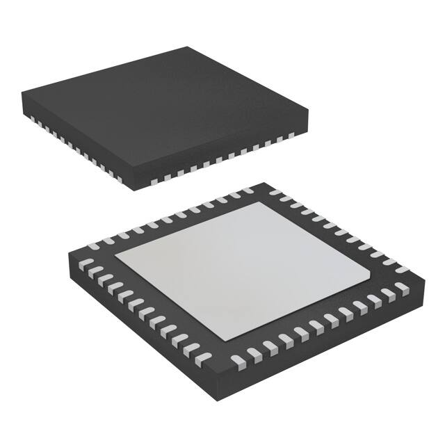


 工商网监
湘ICP备2023018690号
工商网监
湘ICP备2023018690号
