TPS726126
TPS72615, TPS72616
TPS72618, TPS72625
www.ti.com
SLVS403H – MAY 2002 – REVISED JUNE 2010
LOW INPUT VOLTAGE,
1-A LOW-DROPOUT LINEAR REGULATORS
WITH SUPERVISOR
Check for Samples: TPS726126, TPS72615, TPS72616, TPS72618, TPS72625
FEATURES
1
•
•
•
•
•
•
•
•
•
•
1-A Low-Dropout Regulator Supports Input
Voltages Down to 1.8-V
Available in 1.26-V, 1.5-V, 1.6-V, 1.8-V, 2.5-V
Stable With Any Type/Value Output Capacitor
±2% Output Voltage Tolerance Over Line,
Load, and Temperature (–40°C to +125°C)
Integrated Supervisor (SVS) With 200-ms
RESET Delay Time
Low 170-mV Dropout Voltage at 1 A
(TPS72625)
Low 210-mA Ground Current at Full Load
Less than 1-mA Standby Current
Integrated UVLO with Thermal and
Overcurrent Protection
5-Lead SOT223 or DDPAK Surface-Mount
Package
APPLICATIONS
•
•
•
•
•
PCI Cards
Modem Banks and Telecom Boards
DSP, FPGA, and Microprocessor Power
Supplies
Portable, Battery-Powered Applications
1.26-V Core Voltage for the Following DSPs:
– TMS320vC5501
– TMS320vC5502
DESCRIPTION
The TPS726xx family of 1-A low-dropout (LDO) linear
regulators has fixed voltage options available that are
commonly used to power the latest DSPs, FPGAs,
and microcontrollers. The integrated supervisory
circuitry provides an active low RESET signal when
the output falls out of regulation. The no
capacitor/any capacitor feature allows the customer
to tailor output transient performance as needed.
Therefore, compared to other regulators capable of
providing the same output current, this family of
regulators can provide a stand alone power supply
solution or a post regulator for a switch mode power
supply.
These regulators operate over a wide range of input
voltages (1.8 V to 6 V) and have very low dropout
(170 mV at 1-A). Ground current is typically 210 µA at
full load and drops to less than 80 µA at no load.
Standby current is less than 1 µA.
Unlike some regulators that have a minimum current
requirement, the TPS726xx family is stable with no
output load current. The low noise capability of this
family, coupled with its high current operation and
ease of power dissipation, make it ideal for telecom
boards, modem banks, and other noise sensitive
applications.
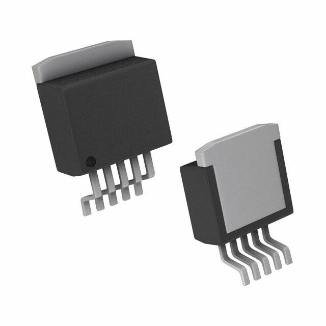
The TPS726xx is available in either a SOT223 or
DDPAK package. The TPS726126 is available in a
SOT223 package only.
DCQ PACKAGE
SOT223-5
(TOP VIEW)
1
2
3
4
5
1 2 3 4 5
ENABLE
IN
GND
OUT
RESET
ENABLE
IN
GND
OUT
RESET
KTT PACKAGE
DDPAK
(TOP VIEW)
Note: Tab is GND for both packages
1
Please be aware that an important notice concerning availability, standard warranty, and use in critical applications of Texas
Instruments semiconductor products and disclaimers thereto appears at the end of this data sheet.
PRODUCTION DATA information is current as of publication date.
Products conform to specifications per the terms of the Texas
Instruments standard warranty. Production processing does not
necessarily include testing of all parameters.
Copyright © 2002–2010, Texas Instruments Incorporated
�TPS726126
TPS72615, TPS72616
TPS72618, TPS72625
SLVS403H – MAY 2002 – REVISED JUNE 2010
www.ti.com
This integrated circuit can be damaged by ESD. Texas Instruments recommends that all integrated circuits be handled with
appropriate precautions. Failure to observe proper handling and installation procedures can cause damage.
ESD damage can range from subtle performance degradation to complete device failure. Precision integrated circuits may be more
susceptible to damage because very small parametric changes could cause the device not to meet its published specifications.
ORDERING INFORMATION (1)
PRODUCT
VOUT
TPS726xx xyyy z
(1)
XXX is nominal output voltage (for example, 126 = 1.26V, 15 = 1.5V).
YYY is package designator.
Z is package quantity.
For the most current package and ordering information, see the Package Option Addendum at the end of this document, or see the TI
website at www.ti.com.
ABSOLUTE MAXIMUM RATINGS
over operating free-air temperature range unless otherwise noted (1)
UNIT
Input voltage, VI
(2)
Voltage range at EN
–0.3 to 7
V
–0.3 to VI + 0.3
V
VIN + 0.3
V
6
V
2
kV
Voltage on RESET
Voltage on OUT
ESD rating, HBM
Continuous total power dissipation
See Dissipation Rating Table
Operating junction temperature range, TJ
–50 to 150
°C
Maximum junction temperature range, TJ
150
°C
–65 to 150
°C
Storage temperature, Tstg
(1)
(2)
Stresses beyond those listed under absolute maximum ratings may cause permanent damage to the device. These are stress ratings
only, and functional operation of the device at these or any other conditions beyond those indicated under recommended operating
conditions is not implied. Exposure to absolute-maximum-rated conditions for extended periods may affect device reliability.
All voltage values are with respect to network ground terminal.
PACKAGE DISSIPATION RATINGS
(1)
(2)
2
PACKAGE
BOARD
RqJC
RqJA
DDPAK
High K (1)
2 °C/W
23 °C/W
SOT223
Low K (2)
15 °C/W
53 °C/W
The JEDEC high K (2s2p) board design used to derive this data was a 3-inch x 3-inch (7,5-cm x 7,5-cm), multilayer board with 1 ounce
internal power and ground planes and 2 ounce copper traces on top and bottom of the board.
The JEDEC low K (1s) board design used to derive this data was a 3-inch x 3-inch (7,5-cm x 7,5-cm), two-layer board with 2 ounce
copper traces on top of the board.
Submit Documentation Feedback
Copyright © 2002–2010, Texas Instruments Incorporated
Product Folder Link(s): TPS726126 TPS72615 TPS72616 TPS72618 TPS72625
�TPS726126
TPS72615, TPS72616
TPS72618, TPS72625
www.ti.com
SLVS403H – MAY 2002 – REVISED JUNE 2010
ELECTRICAL CHARACTERISTICS
over recommended operating free-air temperature range VI = VO(typ) + 1 V, IO= 1 mA, EN = IN, CO = 1 µF, CI = 1 µF (unless
otherwise noted). Typical values are at +25°C.
PARAMETER
VI
(1)
IO
TEST CONDITIONS
Input voltage
Continuous output current
Bandgap voltage reference
VO
Output voltage
I
MIN
6
V
0
1
A
V
1.177
1.220
1.263
1.222
1.26
1.298
1.8 V ≤ VI ≤ 5.5 V
TPS72615
0 µA < IO < 1 A
1.8 V ≤ VI ≤ 5.5 V
1.47
1.5
1.53
TPS72616
0 µA < IO < 1 A
2.6 V ≤ VI ≤ 5.5 V
1.568
1.6
1.632
TPS72618
0 µA < IO < 1 A
2.8 V ≤ VI ≤ 5.5 V
1.764
1.8
1.836
TPS72625
0 µA < IO < 1 A
3.5 V ≤ VI ≤ 5.5 V
2.45
2.5
2.55
IO = 0 µA
75
120
IO = 1 A
210
300
0.2
1
Standby current
EN < 0.4 V
Output noise voltage
BW = 200 Hz to 100 kHz
PSRR
Ripple rejection
f = 1 kHz, Co = 10 µF
Current limit (2)
CO = 10 µF
150
µA
dB
1.6
2.3
A
Output voltage line regulation
(ΔVO/VO) (3)
VO + 1 V < VI ≤ 5.5 V
–0.15
0.02
0.15
%/V
Output voltage load regulation
0 µA < IO < 1 A
–0.25
0.05
0.25
%/A
EN high level input
1.3
EN low level input
–0.2
II
EN input current
EN = 0 V or VI
UVLO threshold
VCC rising
UVLO hysteresis
VCC rising
UVLO deglitch
UVLO delay
Dropout voltage
(4)
1.45
0.4
0.01
100
1.57
1.70
V
nA
V
50
mV
VCC rising
10
µs
VCC rising
100
µs
TPS72625
IO = 1 A
170
280
TPS72618
IO = 1 A
210
320
Minimum input voltage for valid
RESET (VRES)
1.3
Trip threshold voltage
90
Hysteresis voltage
t(RESET) delay time
100
Output low voltage (at 700 µA)
93
96
Leakage current
Operating junction temperature
200
–40
%VO
mV
300
10
–0.3
mV
V
10
Rising edge deglitch
(4)
µA
1.1
VIL
(1)
(2)
(3)
V
µV
60
VIH
TJ
UNIT
1.8
0 µA < IO < 1 A
Vn
RESET
MAX
TPS726126
Ground current
VDO
TYP
ms
µs
0.4
V
100
nA
+125
°C
Minimum VIN is 1.800 V or VO + VDO, whichever is greater.
Test condition includes, output voltage VO = VO – 15% and pulse duration = 10 ms.
VImin = (VO + 1) or 1.8 V whichever is greater.
VOǒ5.5 V * V IminǓ
Line regulation (mV) + (%ńV)
1000
100
Dropout voltage is defined as the differential voltage between VO and VI when VO drops 100 mV below the value measured with
VI = VO + 1 V.
Copyright © 2002–2010, Texas Instruments Incorporated
Submit Documentation Feedback
Product Folder Link(s): TPS726126 TPS72615 TPS72616 TPS72618 TPS72625
3
�TPS726126
TPS72615, TPS72616
TPS72618, TPS72625
SLVS403H – MAY 2002 – REVISED JUNE 2010
www.ti.com
FUNCTIONAL BLOCK DIAGRAM
TPS726126/15/16
IN
OUT
EN
Current Limit
/ Thermal
Protection
1.220
Vref
GND
RESET
Deglitch
and
Delay
0.93 × Vref
Terminal Functions
TERMINAL
NAME
NO.
DESCRIPTION
GND
3
Ground
ENABLE
1
Enable input
IN
2
Input supply voltage
RESET
5
This terminal is the RESET output. When used with a pull-up resistor, this open-drain output provides the active low
RESET signal when the regulator output voltage drops more than 5% below its nominal output voltage. The RESET
delay time is typically 200 ms.
OUT
4
Regulated output voltage
RESET TIMING DIAGRAM
IN
VRES
(see Note A)
VRES
t
OUT
VIT +
VIT +
Threshold
Voltage
VIT −
Î
Î
Î
Î
Î
Î
RESET
Output
Output
Undefined
VIT −
t
200 ms
Delay
200 ms
Delay
Submit Documentation Feedback
Output
Undefined
t
NOTES:A. VRES is the minimum input voltage for a valid RESET.
4
Î
Î
Î
Î
Î
Î
Copyright © 2002–2010, Texas Instruments Incorporated
Product Folder Link(s): TPS726126 TPS72615 TPS72616 TPS72618 TPS72625
�TPS726126
TPS72615, TPS72616
TPS72618, TPS72625
www.ti.com
SLVS403H – MAY 2002 – REVISED JUNE 2010
TYPICAL CHARACTERISTICS
TPS72618
OUTPUT VOLTAGE
vs
JUNCTION TEMPERATURE
TPS72618 OUTPUT VOLTAGE
vs
OUTPUT CURRENT
250
1.805
1.8015
V O − Output Voltage − V
1.8005
1.8
1.7995
Ground Current − µ A
VI = 2.8 V
Co = 1 µF
VI = 2.8 V
Co = 1 µF
TJ = 25° C
1.801
V O − Output Voltage − V
TPS72618
GROUND CURRENT
vs
JUNCTION TEMPERATURE
1.800
IO = 0 mA
1.795
IO = 1 A
1.790
IO = 1 A
150
IO = 0 mA
100
50
1.799
1.785
−40−25 −10 5 20 35 50 65 80 95 110 125
TJ − Junction Temperature − °C
1.7985
0.2
0.4
0.6
0.8
1
IO − Output Current − A
20 35 50 65 80 95 110 125
TJ − Junction Temperature − °C
Figure 1.
Figure 2.
Figure 3.
TPS72618
GROUND CURRENT
vs
OUTPUT CURRENT
TPS72625
DC DROPOUT VOLTAGE
vs
OUTPUT CURRENT
TPS72618
DROPOUT VOLTAGE
vs
JUNCTION TEMPERATURE
300
200
300
VO = 2.5 V (nom)
175
V DO − Dropout Voltage − mV
250
150
125
100
75
50
25
0
0.01
0
−40 −25 −10 5
V DO − Dropout Voltage − mV
0
Ground Current − µ A
200
VI = 2.8 V
Co = 1 µF
TJ = 25° C
TJ = 125°C
200
TJ = 25°C
150
100
TJ = −40°C
50
0
0.1
1
10
100
1000
IO − Output Current − mA
Figure 4.
Copyright © 2002–2010, Texas Instruments Incorporated
0
0.2
0.4
0.6
0.8
IO − Output Current − A
1
250
VO = 1.7 V
Co = 1 µF
IO = 1 A
200
150
100
50
IO = 10 mA
0
−40 −25 −10 5
20 35 50 65 80 95 110 125
TJ − Junction Temperature − °C
Figure 5.
Figure 6.
Submit Documentation Feedback
Product Folder Link(s): TPS726126 TPS72615 TPS72616 TPS72618 TPS72625
5
�TPS726126
TPS72615, TPS72616
TPS72618, TPS72625
SLVS403H – MAY 2002 – REVISED JUNE 2010
www.ti.com
TYPICAL CHARACTERISTICS (continued)
MINIMUM REQUIRED
INPUT VOLTAGE
vs
OUTPUT VOLTAGE
TJ = 125°C
TJ = 25°C
2.5
TJ = −40°C
2
1.5
2
2.5
3
3.5
4
4.5
−100
0
50 100 150 200 250 300 350 400 450 500
−100
1
0.5
0
0
5
t − Time − µs
10 15 20 25 30 35 40 45 50
t − Time − µs
Figure 9.
TPS72618
LOAD TRANSIENT
RESPONSE
TPS72618
OUTPUT VOLTAGE,
ENABLE VOLTAGE
vs
TIME (START-UP)
TPS72618
POWER UP/POWER DOWN
−100
VI = 2.8 V
Co = 1 µF
CI = 1 µF
1
0.5
0
10
15 20 25 30 35 40
t − Time − µs
45 50
Figure 10.
Submit Documentation Feedback
3
VI − Input Voltage − V
0
5
0
0
Figure 8.
100
0
100
VO = 2.8 V
Co = 10 µF
Ci = 1 µF
100
Figure 7.
Enable Voltage − V
∆VO − Change in
I O − Output Current − A Output Voltage − mV
VO − Output Voltage − V
VO − Output Voltage − mV
3
1.5
6
2.8
VI = 2.8 V
IO = 1 A
Co = 10 µF
2
1
0
2
1.5
1
0.5
0
0
20 40 60
80 100 120 140 160 180 200
t − Time − µs
VO − Output Voltage − V
3.5
IO = 1 A
Co = 10 µF
3.8
I O − Output Current − A
VI − Input Voltage − V
4
V − Output Voltage − V
O
V I − Minimum Required Input Voltage − V
4.5
TPS72618
LOAD TRANSIENT
RESPONSE
∆VO − Change in
Output Voltage − mV
TPS72618
LINE TRANSIENT
RESPONSE
5
4
3
RL = 1.8 Ω
Co = 1 µF
Ci = 1 µF
VI
2
1
0
VO
0 100 200 300 400 500 600 700 800 900 1000
Figure 11.
t − Time − µs
Figure 12.
Copyright © 2002–2010, Texas Instruments Incorporated
Product Folder Link(s): TPS726126 TPS72615 TPS72616 TPS72618 TPS72625
�TPS726126
TPS72615, TPS72616
TPS72618, TPS72625
www.ti.com
SLVS403H – MAY 2002 – REVISED JUNE 2010
TYPICAL CHARACTERISTICS (continued)
TPS72618
RIPPLE REJECTION
vs
FREQUENCY
2.5
2000
VI= 2.8 V,
VO = 1.8 V,
CO = 10 µF
90
2
IO = 1 A
1.5
1
80
60
10 µF / 1mA
50
IO = 1 mA
40
30
10 µF / 1A
10
100
1k
10 k
f − Frequency − Hz
1500
TJ = 25°C
1400
TJ = −40°C
1300
1100
10
Figure 13.
100
1k
10 k
100 k
1M
2
2.5
3
3.5
4
4.5
f − Frequency − Hz
VI − Input voltage − V
Figure 14.
Figure 15.
TPS72615
GROUND CURRENT
vs
INPUT VOLTAGE
5
5.5
DROPOUT VOLTAGE
vs
INPUT VOLTAGE
600
300
500
250
V DO − Dropout Voltage − mV
Ground Current − µ A
1600
1000
1.5
0
100 k
1700
1200
10
0
TJ = 125°C
1800
70
20
0.5
1900
Current Limit − A
3
CURRENT LIMIT
vs
INPUT VOLTAGE
100
VI = 2.8 V
Co = 10 µF
Ripple Rejection − dB
µ V/
3.5
Output Spectral Noise Density −
Hz
TPS72618
OUTPUT SPECTRAL NOISE
DENSITY
vs
FREQUENCY
400
300
I=1A
200
I=0A
100
0
TJ = 125°C
TJ = 25°C
200
150
100
TJ = −40°C
50
0
0
1
2
3
4
5
VI − Input Voltage − V
Figure 16.
Copyright © 2002–2010, Texas Instruments Incorporated
6
1.5
2
2.5 3
3.5 4
4.5
VI − Input Voltage − V
5
5.5
Figure 17.
Submit Documentation Feedback
Product Folder Link(s): TPS726126 TPS72615 TPS72616 TPS72618 TPS72625
7
�TPS726126
TPS72615, TPS72616
TPS72618, TPS72625
SLVS403H – MAY 2002 – REVISED JUNE 2010
www.ti.com
APPLICATION INFORMATION
The TPS726xx family of low-dropout (LDO) regulators have numerous features that make it apply to a wide
range of applications. The family operates with very low input voltage (≥1.8 V) and low dropout voltage (typically
200 mV at full load), making it an efficient stand-alone power supply or post regulator for battery or switch mode
power supplies. Both the active low RESET and 1-A output current, make the TPS726xx family ideal for
powering processor and FPGA supplies. The TPS726xx family also has low output noise (typically 150 µVRMS
with 10-µF output capacitor), making it ideal for use in telecom equipment.
External Capacitor Requirements
A 1-µF or larger ceramic input bypass capacitor, connected between IN and GND and located close to the
TPS726xx, is required for stability. To improve transient response, noise rejection, and ripple rejection, an
additional 10-µF or larger, low ESR capacitor is recommended. A higher-value, low ESR input capacitor may be
necessary if large, fast-rise-time load transients are anticipated and the device is located several inches from the
power source, especially if the minimum input voltage of 1.8 V is used.
Although an output capacitor is not required for stability, transient response and output noise are improved with a
10-µF output capacitor.
TPS726xx
VI
IN
VO
OUT
1 mF
10 kW
EN
CO
RESET
GND
Figure 18. TPS726xx Fixed Output Typical Application Diagram
Regulator Protection
The TPS726xx pass element has a built-in back diode that safely conducts reverse current when the input
voltage drops below the output voltage (e.g., during power down). Current is conducted from the output to the
input and is not internally limited. If extended reverse voltage is anticipated, external limiting might be
appropriate.
The TPS726xx also features internal current limiting and thermal protection. During normal operation, the
TPS726xx limits output current to approximately 1.6 A. When current limiting engages, the output voltage scales
back linearly until the overcurrent condition ends. While current limiting is designed to prevent gross device
failure, care should be taken not to exceed the power dissipation ratings of the package. If the temperature of the
device exceeds 165°C, thermal-protection circuitry shuts it down. Once the device has cooled down to below
145°C, regulator operation resumes.
THERMAL INFORMATION
The amount of heat that an LDO linear regulator generates is directly proportional to the amount of power it
dissipates during operation. All integrated circuits have a maximum allowable junction temperature (TJmax)
above which normal operation is not assured. A system designer must design the operating environment so that
the operating junction temperature (TJ) does not exceed the maximum junction temperature (TJmax). The two
main environmental variables that a designer can use to improve thermal performance are air flow and external
heatsinks. The purpose of this information is to aid the designer in determining the proper operating environment
for a linear regulator that is operating at a specific power level.
8
Submit Documentation Feedback
Copyright © 2002–2010, Texas Instruments Incorporated
Product Folder Link(s): TPS726126 TPS72615 TPS72616 TPS72618 TPS72625
�TPS726126
TPS72615, TPS72616
TPS72618, TPS72625
www.ti.com
SLVS403H – MAY 2002 – REVISED JUNE 2010
In general, the maximum expected power (PD(max)) consumed by a linear regulator is computed as:
ǒ
P max + V
*V
D
I(avg)
O(avg)
Ǔ
I
) V
O(avg)
I(avg)
xI
(Q)
(1)
Where:
• VI(avg) is the average input voltage.
• VO(avg) is the average output voltage.
• O(avg) is the average output current.
• I(Q) is the quiescent current.
For most TI LDO regulators, the quiescent current is insignificant compared to the average output current;
therefore, the term VI(avg) x I(Q) can be neglected. The operating junction temperature is computed by adding the
ambient temperature (TA) and the increase in temperature due to the regulator's power dissipation. The
temperature rise is computed by multiplying the maximum expected power dissipation by the sum of the thermal
resistances between the junction and the case ®qJC), the case to heatsink ®qCS), and the heatsink to ambient
®qSA). Thermal resistances are measures of how effectively an object dissipates heat. Typically, the larger the
device, the more surface area available for power dissipation and the lower the object's thermal resistance.
Figure 19 illustrates these thermal resistances for (a) a SOT223 package mounted in a JEDEC low-K board, and
(b) a DDPAK package mounted on a JEDEC high-K board.
A
TJ
RθJC
CIRCUIT BOARD COPPER AREA
C
B
B
A
B
TC
RθCS
A
C
RθSA
SOT223 Package
(a)
TA
DDPAK Package
(b)
C
Figure 19. Thermal Resistances
Equation 2 summarizes the computation:
T
J
ǒ
+ T ) PDmax x R
) R
) R
A
θJC
θCS
θSA
Ǔ
(2)
The RqJC is specific to each regulator as determined by its package, lead frame, and die size provided in the
regulator's data sheet. The RqSA is a function of the type and size of heatsink. For example, black body radiator
type heatsinks can have RqCS values ranging from 5°C/W for very large heatsinks to 50°C/W for very small
heatsinks. The RqCS is a function of how the package is attached to the heatsink. For example, if a thermal
compound is used to attach a heatsink to a SOT223 package, RqCSof 1°C/W is reasonable.
Even if no external black body radiator type heatsink is attached to the package, the board on which the
regulator is mounted provides some heatsinking through the pin solder connections. Some packages, like the
DDPAK and SOT223 packages, use a copper plane underneath the package or the circuit board's ground plane
for additional heatsinking to improve their thermal performance. Computer-aided thermal modeling can be used
to compute very accurate approximations of an integrated circuit's thermal performance in different operating
environments (e.g., different types of circuit boards, different types and sizes of heatsinks, and different air flows,
etc.). Using these models, the three thermal resistances can be combined into one thermal resistance between
junction and ambient ®qJA). This RqJAis valid only for the specific operating environment used in the computer
model.
Copyright © 2002–2010, Texas Instruments Incorporated
Submit Documentation Feedback
Product Folder Link(s): TPS726126 TPS72615 TPS72616 TPS72618 TPS72625
9
�TPS726126
TPS72615, TPS72616
TPS72618, TPS72625
SLVS403H – MAY 2002 – REVISED JUNE 2010
www.ti.com
Equation 2 simplifies into Equation 3:
T + T ) PDmax x R
J
A
θJA
(3)
Rearranging Equation 3 gives Equation 4:
T –T
R
+ J A
θJA
P max
D
(4)
Using Equation 3 and the computer model generated curves shown in Figure 20 and Figure 23, a designer can
quickly compute the required heatsink thermal resistance/board area for a given ambient temperature, power
dissipation, and operating environment.
DDPAK Power Dissipation
The DDPAK package provides an effective means of managing power dissipation in surface mount applications.
The DDPAK package dimensions are provided in the Mechanical Data section at the end of the data sheet. The
addition of a copper plane directly underneath the DDPAK package enhances the thermal performance of the
package.
To illustrate, the TPS72625 in a DDPAK package was chosen. For this example, the average input voltage is 5
V, the output voltage is 2.5 V, the average output current is 1 A, the ambient temperature 55°C, the air flow is
150 LFM, and the operating environment is the same as documented below. Neglecting the quiescent current,
the maximum average power is:
P Dmax + (5 * 2.5) V x 1 A + 2.5 W
(5)
Substituting TJmax for TJ into Equation 4 gives Equation 6:
R
max + (125 * 55)°Cń2.5 W + 28°CńW
θJA
(6)
2
From Figure 20, DDPAK Thermal Resistance vs Copper Heatsink Area, the ground plane needs to be 1 cm for
the part to dissipate 2.5 W. The operating environment used in the computer model to construct Figure 20
consisted of a standard JEDEC High-K board (2S2P) with a 1 oz. internal copper plane and ground plane. The
package is soldered to a 2 oz. copper pad. The pad is tied through thermal vias to the 1 oz. ground plane.
Figure 21 shows the side view of the operating environment used in the computer model.
40
Rθ JA − Thermal Resistance −
° C/W
No Air Flow
35
150 LFM
30
250 LFM
25
20
15
0.1
1
10
Copper Heatsink Area − cm2
100
Figure 20. DDPAK Thermal Resistance vs Copper Heatsink Area
10
Submit Documentation Feedback
Copyright © 2002–2010, Texas Instruments Incorporated
Product Folder Link(s): TPS726126 TPS72615 TPS72616 TPS72618 TPS72625
�TPS726126
TPS72615, TPS72616
TPS72618, TPS72625
www.ti.com
SLVS403H – MAY 2002 – REVISED JUNE 2010
2 oz. Copper Solder Pad
with 25 Thermal Vias
1 oz. Copper
Power Plane
1 oz. Copper
Ground Plane
Thermal Vias, 0,3 mm
Diameter, 1,5 mm Pitch
Figure 21. DDPAK Thermal Resistance
From the data in Figure 22 and rearranging Equation 4, the maximum power dissipation for a different ground
plane area and a specific ambient temperature can be computed.
TJM − Maximum Junction Temperature − 125 °C
5
PD − Maximum Power Dissipation − W
TA = 55°C
4
250 LFM
150 LFM
3
No Air Flow
2
1
0.1
1
10
Copper Heatsink Area − cm2
100
Figure 22. Maximum Power Dissipation vs Copper Heatsink Area
SOT223 Power Dissipation
The SOT223 package provides an effective means of managing power dissipation in surface mount applications.
The SOT223 package dimensions are provided in the Mechanical Data section at the end of the data sheet. The
addition of a copper plane directly underneath the SOT223 package enhances the thermal performance of the
package.
To illustrate, the TPS72625 in a SOT223 package was chosen. For this example, the average input voltage is
3.3 V, the output voltage is 2.5 V, the average output current is 1 A, the ambient temperature 55°C, no air flow is
present, and the operating environment is the same as documented below. Neglecting the quiescent current, the
maximum average power is:
P Dmax + (3.3 * 2.5) V x 1 A + 800 mW
(7)
Substituting TJmax for TJ into Equation 4 gives Equation 8:
Copyright © 2002–2010, Texas Instruments Incorporated
Submit Documentation Feedback
Product Folder Link(s): TPS726126 TPS72615 TPS72616 TPS72618 TPS72625
11
�TPS726126
TPS72615, TPS72616
TPS72618, TPS72625
SLVS403H – MAY 2002 – REVISED JUNE 2010
R
θJA
www.ti.com
max + (125 * 55)°Cń800 mW + 87.5°CńW
(8)
2
From Figure 23, RqJA vs PCB Copper Area, the ground plane needs to be 0.55 in for the part to dissipate 800
mW. The operating environment used to construct Figure 23 consisted of a board with 1 oz. copper planes. The
package is soldered to a 1 oz. copper pad on the top of the board. The pad is tied through thermal vias to the 1
oz. ground plane.
Rθ JA − Thermal Resistance −
° C/W
180
No Air Flow
160
140
120
100
80
60
40
20
0
0.1
1
PCB Copper Area − in2
10
Figure 23. SOT223 Thermal Resistance vs PCB AREA
From the data in Figure 23 and rearranging Equation 4, the maximum power dissipation for a different ground
plane area and a specific ambient temperature can be computed (as shown in Figure 24).
6
PD − Maximum Power Dissipation − W
TA = 25°C
5
4
4 in2 PCB Area
3
0.5 in2 PCB Area
2
1
0
0
25
50
75
100
125
150
TA − Ambient Temperature − °C
Figure 24. SOT223 Power Dissipation
12
Submit Documentation Feedback
Copyright © 2002–2010, Texas Instruments Incorporated
Product Folder Link(s): TPS726126 TPS72615 TPS72616 TPS72618 TPS72625
�TPS726126
TPS72615, TPS72616
TPS72618, TPS72625
www.ti.com
SLVS403H – MAY 2002 – REVISED JUNE 2010
REVISION HISTORY
NOTE: Page numbers for previous revisions may differ from page numbers in the current version.
Changes from Revision G (May 2006) to Revision H
Page
•
Deleted Figure 14, Output Impedance vs Frequency ........................................................................................................... 7
•
Added Figure 18 ................................................................................................................................................................... 8
Copyright © 2002–2010, Texas Instruments Incorporated
Submit Documentation Feedback
Product Folder Link(s): TPS726126 TPS72615 TPS72616 TPS72618 TPS72625
13
�PACKAGE OPTION ADDENDUM
www.ti.com
14-Oct-2022
PACKAGING INFORMATION
Orderable Device
Status
(1)
Package Type Package Pins Package
Drawing
Qty
Eco Plan
(2)
Lead finish/
Ball material
MSL Peak Temp
Op Temp (°C)
Device Marking
(3)
Samples
(4/5)
(6)
TPS726126DCQ
ACTIVE
SOT-223
DCQ
6
78
RoHS & Green
NIPDAU
Level-2-260C-1 YEAR
-40 to 125
726126
Samples
TPS726126DCQR
ACTIVE
SOT-223
DCQ
6
2500
RoHS & Green
NIPDAU
Level-2-260C-1 YEAR
-40 to 125
726126
Samples
TPS72615DCQ
ACTIVE
SOT-223
DCQ
6
78
RoHS & Green
NIPDAU
Level-2-260C-1 YEAR
-40 to 125
PS72615
Samples
TPS72615DCQR
ACTIVE
SOT-223
DCQ
6
2500
RoHS & Green
NIPDAU
Level-2-260C-1 YEAR
-40 to 125
PS72615
Samples
TPS72615KTTR
ACTIVE
DDPAK/
TO-263
KTT
5
500
RoHS & Green
Call TI | SN
Level-2-260C-1 YEAR
-40 to 125
TPS
72615
Samples
TPS72616DCQ
ACTIVE
SOT-223
DCQ
6
78
RoHS & Green
NIPDAU
Level-2-260C-1 YEAR
-40 to 125
PS72616
Samples
TPS72616DCQR
ACTIVE
SOT-223
DCQ
6
2500
RoHS & Green
NIPDAU
Level-2-260C-1 YEAR
-40 to 125
PS72616
Samples
TPS72616KTTR
ACTIVE
DDPAK/
TO-263
KTT
5
500
RoHS & Green
Call TI | SN
Level-2-260C-1 YEAR
TPS
72616
Samples
TPS72616KTTRG3
ACTIVE
DDPAK/
TO-263
KTT
5
500
RoHS & Green
SN
Level-2-260C-1 YEAR
TPS
72616
Samples
TPS72618DCQ
ACTIVE
SOT-223
DCQ
6
78
RoHS & Green
NIPDAU
Level-2-260C-1 YEAR
PS72618
Samples
TPS72618DCQR
ACTIVE
SOT-223
DCQ
6
2500
RoHS & Green
NIPDAU
Level-2-260C-1 YEAR
PS72618
Samples
TPS72618KTTR
ACTIVE
DDPAK/
TO-263
KTT
5
500
RoHS & Green
Call TI | SN
Level-2-260C-1 YEAR
TPS
72618
Samples
TPS72625DCQ
ACTIVE
SOT-223
DCQ
6
78
RoHS & Green
NIPDAU
Level-2-260C-1 YEAR
PS72625
Samples
TPS72625DCQR
ACTIVE
SOT-223
DCQ
6
2500
RoHS & Green
NIPDAU
Level-2-260C-1 YEAR
PS72625
Samples
TPS72625KTTT
ACTIVE
DDPAK/
TO-263
KTT
5
50
RoHS & Green
Call TI | SN
Level-2-260C-1 YEAR
TPS
72625
Samples
(1)
The marketing status values are defined as follows:
ACTIVE: Product device recommended for new designs.
LIFEBUY: TI has announced that the device will be discontinued, and a lifetime-buy period is in effect.
NRND: Not recommended for new designs. Device is in production to support existing customers, but TI does not recommend using this part in a new design.
PREVIEW: Device has been announced but is not in production. Samples may or may not be available.
OBSOLETE: TI has discontinued the production of the device.
Addendum-Page 1
-40 to 125
�PACKAGE OPTION ADDENDUM
www.ti.com
14-Oct-2022
(2)
RoHS: TI defines "RoHS" to mean semiconductor products that are compliant with the current EU RoHS requirements for all 10 RoHS substances, including the requirement that RoHS substance
do not exceed 0.1% by weight in homogeneous materials. Where designed to be soldered at high temperatures, "RoHS" products are suitable for use in specified lead-free processes. TI may
reference these types of products as "Pb-Free".
RoHS Exempt: TI defines "RoHS Exempt" to mean products that contain lead but are compliant with EU RoHS pursuant to a specific EU RoHS exemption.
Green: TI defines "Green" to mean the content of Chlorine (Cl) and Bromine (Br) based flame retardants meet JS709B low halogen requirements of


 工商网监
湘ICP备2023018690号
工商网监
湘ICP备2023018690号
