Sample &
Buy
Product
Folder
Support &
Community
Tools &
Software
Technical
Documents
Reference
Design
TPS7A8001
SBVS135I – JUNE 2010 – REVISED AUGUST 2015
TPS7A8001 Low-Noise, Wide-Bandwidth, High PSRR,
Low-Dropout 1A Linear Regulator
1 Features
3 Description
•
•
•
The TPS7A8001 is a low-dropout linear regulator
(LDO) offering very high power-supply ripple rejection
(PSRR) at the output. This LDO uses an advanced
BiCMOS process and a PMOSFET pass device to
achieve very low noise, excellent transient response,
and excellent PSRR performance.
1
•
•
•
•
•
•
•
Low-Dropout 1-A Regulator With Enable
Adjustable Output Voltages: 0.8 V to 6 V
Wide-Bandwidth High PSRR:
– 63 dB at 1 kHz
– 57 dB at 100 kHz
– 38 dB at 1 MHz
Low Noise: (14 × VOUT ) μVRMS Typical (100 Hz to
100 kHz)
Stable with a 4.7-μF Ceramic Capacitor
Excellent Load/Line Transient Response
3% Overall Accuracy (Over Load/Line/Temp)
Overcurrent and Overtemperature Protection
Very Low Dropout: 170 mV Typical at 1 A
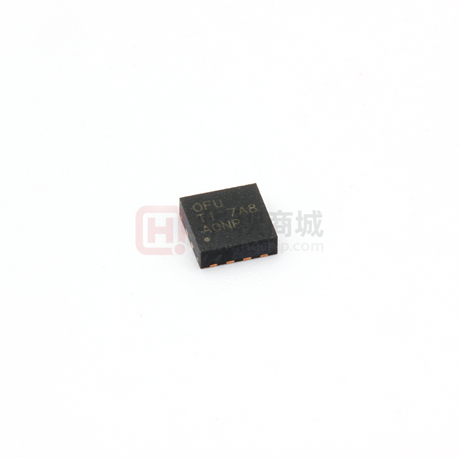
3-mm × 3-mm VSON-8 DRB Package
The TPS7A8001 is stable with a 4.7-μF ceramic
output capacitor, and uses a precision voltage
reference and feedback loop to achieve a worst-case
accuracy of 3% over all load, line, process, and
temperature variations.
This device is fully specified over the temperature
range of TJ = –40°C to 125°C and is offered in a
3mm × 3mm, VSON-8 package with a thermal pad.
Device Information(1)
PART NUMBER
TPS7A80
2 Applications
•
•
•
PACKAGE
VSON (8)
BODY SIZE (NOM)
3.00 mm × 3.00 mm
(1) For all available packages, see the orderable addendum at
the end of the data sheet.
Telecom Infrastructure
Audio
High-Speed I/F (PLL/VCO)
Typical Application Diagram
Optional 1.0mF input capacitor.
May improve source impedance,
noise, or PSRR.
VIN
IN
R1
TPS7A8001
EN
FB
GND
VEN
VOUT
OUT
NR
4.7mF
Ceramic
R2
To avoid inrush current,
it is recommended to
always connect a
1nF to 10nF capacitor
1
An IMPORTANT NOTICE at the end of this data sheet addresses availability, warranty, changes, use in safety-critical applications,
intellectual property matters and other important disclaimers. PRODUCTION DATA.
�TPS7A8001
SBVS135I – JUNE 2010 – REVISED AUGUST 2015
www.ti.com
Table of Contents
1
2
3
4
5
6
7
Features ..................................................................
Applications ...........................................................
Description .............................................................
Revision History.....................................................
Pin Configuration and Functions .........................
Specifications.........................................................
1
1
1
2
4
5
6.1
6.2
6.3
6.4
6.5
6.6
5
5
5
5
6
7
Absolute Maximum Ratings ......................................
ESD Ratings..............................................................
Recommended Operating Conditions.......................
Thermal Information ..................................................
Electrical Characteristics...........................................
Typical Characteristics ..............................................
Detailed Description ............................................ 12
7.1
7.2
7.3
7.4
Overview .................................................................
Functional Block Diagram .......................................
Feature Description.................................................
Device Functional Modes........................................
12
12
12
13
8
Application and Implementation ........................ 14
8.1 Application Information............................................ 14
8.2 Typical Application .................................................. 14
9 Power Supply Recommendations...................... 16
10 Layout................................................................... 17
10.1
10.2
10.3
10.4
10.5
Layout Guidelines .................................................
Layout Example ....................................................
Thermal Considerations ........................................
Power Dissipation .................................................
Estimating Junction Temperature ........................
17
17
17
18
18
11 Device and Documentation Support ................. 20
11.1
11.2
11.3
11.4
Community Resources..........................................
Trademarks ...........................................................
Electrostatic Discharge Caution ............................
Glossary ................................................................
20
20
20
20
12 Mechanical, Packaging, and Orderable
Information ........................................................... 20
4 Revision History
NOTE: Page numbers for previous revisions may differ from page numbers in the current version.
Changes from Revision H (January 2013) to Revision I
Page
•
Added ESD Ratings table, Feature Description section, Device Functional Modes, Application and Implementation
section, Power Supply Recommendations section, Layout section, Device and Documentation Support section, and
Mechanical, Packaging, and Orderable Information section ................................................................................................. 1
•
Deleted "Fixed Output Voltages: 0.8 V to 5 V Using Innovating Facatory EEPROM Programming" bullet from Features ... 1
•
Changed "12.6" to "14" in Low Noise bullet ........................................................................................................................... 1
•
Deleted SNS row from Pin Functions .................................................................................................................................... 4
•
Deleted Fixed Version from VOUT row in Electrical Characteristics ....................................................................................... 6
•
Deleted ISNS row from Electrical Characteristics ................................................................................................................. 6
Changes from Revision G (April 2012) to Revision H
•
Updated Figure 8.................................................................................................................................................................... 7
Changes from Revision F (March 2012) to Revision G
•
Page
Page
Changed Thermal Information table values, added new footnote 2, changed footnote 3...................................................... 5
Changes from Revision E (February 2012) to Revision F
Page
•
Changed Low Noise Features bullet ...................................................................................................................................... 1
•
Updated Equation 3.............................................................................................................................................................. 15
Changes from Revision D (December 2010) to Revision E
Page
•
Changed Low Noise Features bullet ...................................................................................................................................... 1
•
Changed caption of front-page application circuit .................................................................................................................. 1
•
Updated Figure 12.................................................................................................................................................................. 7
2
Submit Documentation Feedback
Copyright © 2010–2015, Texas Instruments Incorporated
Product Folder Links: TPS7A8001
�TPS7A8001
www.ti.com
SBVS135I – JUNE 2010 – REVISED AUGUST 2015
•
Updated Figure 26................................................................................................................................................................ 10
•
Added Equation 1 note in Start-up section........................................................................................................................... 13
•
Updated Equation 3.............................................................................................................................................................. 15
Changes from Revision C (September, 2010) to Revision D
Page
•
Updated front-page figure with new characteristic graph ....................................................................................................... 1
•
Revised Figure 17 .................................................................................................................................................................. 8
•
Changed Figure 18................................................................................................................................................................. 8
Changes from Revision B (August, 2010) to Revision C
Page
•
Changed data sheet title......................................................................................................................................................... 1
•
Changed ultra-high PSRR to wide-bandwidth lhgh PSRR in Features list ............................................................................ 1
•
Corrected typos in Figure 21 through Figure 23 .................................................................................................................... 9
•
Revised first paragraph of Application Information to remove phrase ultra-wide bandwidth ............................................... 14
Submit Documentation Feedback
Copyright © 2010–2015, Texas Instruments Incorporated
Product Folder Links: TPS7A8001
3
�TPS7A8001
SBVS135I – JUNE 2010 – REVISED AUGUST 2015
www.ti.com
5 Pin Configuration and Functions
DRB Package
8-Pin VSON
Top View
OUT
1
8
IN
OUT
2
7
IN
FB/SNS
3
6
NR
GND
4
5
EN
Pin Functions
PIN
NAME
EN
FB
GND
NO.
I/O
DESCRIPTION
I
Driving the enable pin (EN) high turns on the regulator. Driving this pin low puts the regulator into
shutdown mode. Refer to Shutdown in the Application and Implementation section for more details. EN
must not be left floating and can be connected to IN if not used.
3
I
This pin is the input to the control loop error amplifier and is used to set the output voltage of the device.
4, pad
—
5
Ground.
IN
7, 8
I
Unregulated input supply.
OUT
1, 2
O
Regulator output. A 4.7μF or larger capacitor of any type is required for stability.
6
—
Connect an external capacitor between this pin and ground to reduce output noise to very low levels.
Also, the capacitor slows down the VOUT ramp (RC softstart).
NR
4
Submit Documentation Feedback
Copyright © 2010–2015, Texas Instruments Incorporated
Product Folder Links: TPS7A8001
�TPS7A8001
www.ti.com
SBVS135I – JUNE 2010 – REVISED AUGUST 2015
6 Specifications
6.1 Absolute Maximum Ratings
over operating free-air temperature range (unless otherwise noted) (1)
Voltage
Current
(2)
MAX
UNIT
–0.3
7
V
FB, NR
–0.3
3.6
V
EN
–0.3
VIN + 0.3 (2)
V
OUT
–0.3
7
V
OUT
Temperature
(1)
MIN
IN
Internally Limited
A
Operating virtual junction, TJ
–55
150
°C
Storage, Tstg
–55
150
°C
Stresses beyond those listed under Absolute Maximum Ratings may cause permanent damage to the device. These are stress ratings
only, which do not imply functional operation of the device at these or any other conditions beyond those indicated under Recommended
Operating Conditions. Exposure to absolute-maximum-rated conditions for extended periods may affect device reliability.
VEN absolute maximum rating is VIN + 0.3 V or 7 V, whichever is smaller.
6.2 ESD Ratings
VALUE
Human body model (HBM), per ANSI/ESDA/JEDEC JS-001, all pins
V(ESD)
(1)
(2)
Electrostatic discharge
(1)
UNIT
±2000
Charged device model (CDM), per JEDEC specification JESD22-C101, all
pins (2)
V
±500
JEDEC document JEP155 states that 500-V HBM allows safe manufacturing with a standard ESD control process.
JEDEC document JEP157 states that 250-V CDM allows safe manufacturing with a standard ESD control process.
6.3 Recommended Operating Conditions
over operating free-air temperature range (unless otherwise noted)
VI
Input voltage
IO
Output current
TA
Operating free air temperature
MIN
MAX
2.2
6.5
UNIT
V
0
1
A
–40
125
°C
6.4 Thermal Information
TPS7A80xx
THERMAL METRIC (1) (2)
DRB (VSON) (3)
UNIT
8 PINS
RθJA
Junction-to-ambient thermal resistance
47.8
°C/W
RθJC(top)
Junction-to-case (top) thermal resistance
53.9
°C/W
RθJB
Junction-to-board thermal resistance
23.4
°C/W
ψJT
Junction-to-top characterization parameter
1
°C/W
ψJB
Junction-to-board characterization parameter
23.5
°C/W
RθJC(bot)
Junction-to-case (bottom) thermal resistance
7.4
°C/W
(1)
(2)
(3)
For more information about traditional and new thermal metrics, see the Semiconductor and IC Package Thermal Metrics application
report, SPRA953.
For thermal estimates of this device based on PCB copper area, see the TI PCB Thermal Calculator.
Thermal data for the DRB package are derived by thermal simulations based on JEDEC-standard methodology as specified in the
JESD51 series. The following assumptions are used in the simulations:
(a) The exposed pad is connected to the PCB ground layer through a 2 × 2 thermal via array.
(b) The top and bottom copper layers are assumed to have a 5% thermal conductivity of copper representing a 20% copper coverage.
(c) This data were generated with only a single device at the center of a JEDEC high-K (2s2p) board with 3 inches × 3 inches copper
area. To understand the effects of the copper area on thermal performance, refer to the Power Dissipation and Estimating Junction
Temperature sections.
Submit Documentation Feedback
Copyright © 2010–2015, Texas Instruments Incorporated
Product Folder Links: TPS7A8001
5
�TPS7A8001
SBVS135I – JUNE 2010 – REVISED AUGUST 2015
www.ti.com
6.5 Electrical Characteristics
Over the operating temperature range of TJ = –40°C to 125°C, VIN = VOUT(TYP) + 0.5 V or 2.2 V (whichever is greater), IOUT = 1
mA, VEN = 2.2 V, COUT = 4.7 μF, and CNR = 0.01 μF, unless otherwise noted. TPS7A8001 is tested at VOUT = 0.8 V and VOUT =
6 V. Typical values are at TJ = 25°C.
PARAMETER
VIN
Input voltage range (1)
VNR
Internal reference
VOUT
Output voltage range
Output accuracy (2)
TEST CONDITIONS
0.79
VOUT + 0.5 V ≤ VIN ≤ 6.5 V, VIN ≥ 2.2 V,
100 mA ≤ IOUT ≤ 1 A
–3%
100 mA ≤ IOUT ≤ 1 A
Ground pin current
mV
VOUT + 0.5 V ≤ VIN ≤ 6.5 V, VIN ≥ 2.5 V,
IOUT = 750 mA, VFB = GND or VSNS = GND
350
mV
VOUT + 0.5 V ≤ VIN ≤ 6.5 V, VIN ≥ 2.5 V,
IOUT = 1 A, VFB = GND or VSNS = GND
500
mV
1400
2000
mA
60
100
μA
350
μA
VOUT = 0.85 × VOUT(NOM), VIN ≥ 3.3 V
1100
IOUT = 1 mA
IOUT = 1 A
IFB
Feedback pin current
VIN = 6.5 V, VFB = 0.8 V
Output noise voltage
VIN = 4.3 V, VOUT = 3.3 V,
IOUT = 750 mA
BW = 100 Hz to 100 kHz,
VIN = 4.3 V, VOUT = 3.3 V,
IOUT = 100 mA
μA
0.02
1
μA
dB
f = 1 kHz
63
dB
f = 10 kHz
63
dB
f = 100 kHz
57
dB
f = 1 MHz
38
dB
CNR = 0.001
μF
14.6 × VOUT
μVRMS
CNR = 0.01 μF
14.3 × VOUT
μVRMS
13.9 × VOUT
μVRMS
2.2 V ≤ VIN ≤ 3.6 V, RL = 1 kΩ
1.2
V
3.6 V < VIN ≤ 6.5 V, RL = 1 kΩ
1.35
V
Enable high (enabled)
VEN(LO)
Enable low (shutdown)
RL = 1 kΩ
IEN(HI)
Enable pin current, enabled
VIN = VEN = 6.5 V
tSTR
Start-up time
VOUT(NOM) = 3.3 V,
CNR = 1 nF
VOUT = 0% to 90%
VOUT(NOM),
CNR = 10 nF
RL = 3.3 kΩ, COUT = 4.7 μF
Undervoltage lockout
VIN rising, RL = 1 kΩ
Hysteresis
VIN falling, RL = 1 kΩ
TSD
Thermal shutdown
temperature
TJ
Operating junction
temperature
6
2
48
VEN(HI)
(1)
(2)
0.20
f = 100 Hz
CNR = 0.1μF
UVLO
μV/mA
250
Shutdown current (IGND)
VN
μV/V
150
2
ISHDN
Power-supply rejection ratio
3%
VOUT + 0.5 V ≤ VIN ≤ 6.5 V, VIN ≥ 2.2 V,
IOUT = 500 mA, VFB = GND or VSNS = GND
VEN ≤ 0.4 V, VIN ≥ 2.2 V, RL = 1 kΩ, 0°C ≤
TJ ≤ 85°C
PSRR
V
2%
Load regulation
IGND
V
–2%
ΔVOUT/ΔIOUT
Output current limit
V
0.81
6
±0.3%
UNIT
6.5
0.8
VOUT(NOM) + 0.5 V ≤ VIN ≤ 6.5 V, VIN ≥ 2.2 V,
IOUT = 100 mA
ICL
0.8
MAX
VOUT + 0.5 V ≤ VIN ≤ 6 V, VIN ≥ 2.5 V,
100 mA ≤ IOUT ≤ 500 mA, 0°C ≤ TJ ≤ 85°C
Line regulation
Dropout voltage
TYP
2.2
ΔVOUT/ΔVIN
VDO
MIN
0
0.02
1.86
0.4
V
1
μA
0.1
ms
1.6
ms
2
2.10
V
75
mV
Shutdown, temperature increasing
160
°C
Reset, temperature decreasing
140
°C
–40
125
°C
Minimum VIN = VOUT + VDO or 2.2 V, whichever is greater.
As for TPS7A8001 (adjustable); it does not include external resistor tolerances and it is not tested at this condition: VOUT = 0.8 V, 4.5 V
≤ VIN ≤ 6.5 V, and 750 mA ≤ IOUT ≤ 1 A because of power dissipation higher than maximum rating of the package.
Submit Documentation Feedback
Copyright © 2010–2015, Texas Instruments Incorporated
Product Folder Links: TPS7A8001
�TPS7A8001
www.ti.com
SBVS135I – JUNE 2010 – REVISED AUGUST 2015
6.6 Typical Characteristics
At VOUT(TYP) = 3.3 V, VIN = VOUT(TYP) + 0.5 V or 2.2 V (whichever is greater), IOUT = 100 mA, VEN = VIN, CIN = 1 μF, COUT = 4.7 μF, and CNR
= 0.01 μF, all temperature values refer to TJ, unless otherwise noted.
3.399
3.399
+125°C
+85°C
+25°C
0°C
-40°C
3.366
3.366
3.333
VOUT (V)
VOUT (V)
3.333
+125°C
+85°C
+25°C
0°C
-40°C
3.3
3.267
3.3
3.267
3.234
3.234
NOTE: Y axis shows 1% VOUT per division
NOTE: Y axis shows 1% VOUT per division
3.201
3.201
0
100 200 300 400 500 600 700 800 900 1000
IOUT (mA)
0
0.824
+125°C
+85°C
+25°C
0°C
-40°C
20
25
VOUT = 0.8V
IOUT = 5mA
0.816
+125°C
+85°C
+25°C
0°C
-40°C
0.808
VOUT (V)
VOUT (V)
0.818
0.8
0.792
0.8
0.792
0.784
0.784
NOTE: Y axis shows 1% VOUT per division
NOTE: Y axis shows 1% VOUT per division
0.776
0.776
2.2
2.6
3
3.4
3.8
4.2 4.6
VIN (V)
5
5.4
5.8
6.2
2.2
6.6
Figure 3. Line Regulation
500
2.6
3
3.4
3.8
4.2 4.6
VIN (V)
5
5.4
5.8
6.2
6.6
Figure 4. Line Regulation Under Light Loads
500
IOUT = 1A
450
+125°C
+85°C
+25°C
0°C
-40°C
400
350
300
250
200
IOUT = 750mA
450
+125°C
+85°C
+25°C
0°C
-40°C
400
350
VDO (V)
VDO (V)
15
Figure 2. Load Regulation Under Light Loads
VOUT = 0.8V
IOUT = 750mA
0.816
10
IOUT (mA)
Figure 1. Load Regulation
0.824
5
300
250
200
150
150
100
100
50
50
0
0
2
2.5
3
3.5
4
4.5
VIN (V)
5
5.5
6
Figure 5. Dropout Voltage vs Input Voltage
6.5
2
2.5
3
3.5
4
4.5
VIN (V)
5
5.5
6
6.5
Figure 6. Dropout Voltage vs Input Voltage
Submit Documentation Feedback
Copyright © 2010–2015, Texas Instruments Incorporated
Product Folder Links: TPS7A8001
7
�TPS7A8001
SBVS135I – JUNE 2010 – REVISED AUGUST 2015
www.ti.com
Typical Characteristics (continued)
At VOUT(TYP) = 3.3 V, VIN = VOUT(TYP) + 0.5 V or 2.2 V (whichever is greater), IOUT = 100 mA, VEN = VIN, CIN = 1 μF, COUT = 4.7
μF, and CNR = 0.01 μF, all temperature values refer to TJ, unless otherwise noted.
500
500
IOUT = 500mA
450
+125°C
+85°C
+25°C
0°C
-40°C
400
300
250
200
350
300
250
200
150
150
100
100
50
50
0
0
2
2.5
3
3.5
4
4.5
VIN (V)
5
5.5
6
6.5
0
100 200 300 400 500 600 700 800 900 1000
IOUT (mA)
Figure 8. Dropout Voltage vs Load Current
Figure 7. Dropout Voltage vs Input Voltage
500
300
VIN = 3.6V
450
IOUT = 1000mA
IOUT = 750mA
IOUT = 5mA
400
250
200
300
IGND (mA)
VDO (V)
350
250
200
150
100
50
50
0
0
-40 -25 -10
5
20 35 50 65
Temperature (°C)
80
95
VOUT = 0.8V
IOUT = 750mA
2.2
110 125
Figure 9. Dropout Voltage vs Temperature
2.6
3
3.4
3.8
4.2 4.6
VIN (V)
5
5.4
5.8
6.2
6.6
Figure 10. Ground Pin Current vs Input Voltage
2
300
VIN = 2.2V
VIN = 2.5V
VIN = 3V
VIN = 3.3V
1.8
250
1.6
1.4
ISHDN (mA)
200
IGND (mA)
+125°C
+85°C
+25°C
0°C
-40°C
100
150
150
+125°C
+85°C
+25°C
0°C
-40°C
100
50
VIN = 5V
VIN = 5.5V
VIN = 6V
VIN = 6.6V
1.2
1
0.8
0.6
0.4
0.2
VEN = 0.4V
0
0
0
100 200 300 400 500 600 700 800 900 1000
IOUT (mA)
Figure 11. Ground Pin Current vs Load Current
8
+125°C
+85°C
+25°C
0°C
-40°C
400
VDO (V)
VDO (V)
350
VIN = 3.6V
450
-40 -25 -10
5
20 35 50 65
Temperature (°C)
80
95
110 125
Figure 12. Shutdown Current vs Temperature
Submit Documentation Feedback
Copyright © 2010–2015, Texas Instruments Incorporated
Product Folder Links: TPS7A8001
�TPS7A8001
www.ti.com
SBVS135I – JUNE 2010 – REVISED AUGUST 2015
Typical Characteristics (continued)
At VOUT(TYP) = 3.3 V, VIN = VOUT(TYP) + 0.5 V or 2.2 V (whichever is greater), IOUT = 100 mA, VEN = VIN, CIN = 1 μF, COUT = 4.7
μF, and CNR = 0.01 μF, all temperature values refer to TJ, unless otherwise noted.
1800
90
1600
80
1400
70
PSRR (dB)
ICL (mA)
1200
1000
800
600
VIN = 2.2V
VIN = 3.8V
VIN = 5.5V
VIN = 6.5V
400
200
VOUT = VIN - 0.5V
0
50
40
30
IOUT = 100mA
No CIN
20
5
20 35 50 65
Temperature (°C)
80
95
110 125
10
Figure 13. Current Limit vs Temperature
90
80
80
70
70
60
60
50
40
IOUT = 10mA
IOUT = 100mA
IOUT = 750mA
IOUT = 1A
30
20
100
VDO = 1.0V
No CIN
1k
10k
100k
Frequency (Hz)
1M
1k
10k
100k
Frequency (Hz)
1M
10M
VDO = 0.5V
No CIN
50
40
IOUT = 10mA
IOUT = 100mA
IOUT = 750mA
IOUT = 1A
30
10
10
100
Figure 14. Power-Supply Ripple Rejection vs Frequency
90
PSRR (dB)
PSRR (dB)
60
10
-40 -25 -10
20
10
10M
10
100
1k
10k
100k
Frequency (Hz)
1M
10M
Figure 15. Power-Supply Ripple Rejection vs Frequency
Figure 16. Power-Supply Ripple Rejection vs Frequency
90
90
80
80
70
70
60
60
PSRR (dB)
PSRR (dB)
VDO = 1.0V
VDO = 0.5V
VDO = 0.3V
50
40
IOUT = 10mA
IOUT = 100mA
IOUT = 750mA
IOUT = 1A
30
20
VDO = 1.0V
COUT = 100mF
No CIN
10
10
100
1k
10k
100k
Frequency (Hz)
1M
10M
Figure 17. Power-Supply Ripple Rejection vs Frequency
50
40
IOUT = 10mA
IOUT = 100mA
IOUT = 750mA
IOUT = 1A
30
20
VDO = 0.5V
COUT = 100mF
No CIN
10
10
100
1k
10k
100k
Frequency (Hz)
1M
10M
Figure 18. Power-Supply Ripple Rejection vs Frequency
Submit Documentation Feedback
Copyright © 2010–2015, Texas Instruments Incorporated
Product Folder Links: TPS7A8001
9
�TPS7A8001
SBVS135I – JUNE 2010 – REVISED AUGUST 2015
www.ti.com
Typical Characteristics (continued)
At VOUT(TYP) = 3.3 V, VIN = VOUT(TYP) + 0.5 V or 2.2 V (whichever is greater), IOUT = 100 mA, VEN = VIN, CIN = 1 μF, COUT = 4.7
μF, and CNR = 0.01 μF, all temperature values refer to TJ, unless otherwise noted.
90
80
70
70
60
60
50
40
f = 1kHz
f = 10kHz
f = 100kHz
f = 1MHz
30
20
IOUT = 750mA
No CIN
80
PSRR (dB)
PSRR (dB)
90
IOUT = 100mA
No CIN
50
40
f = 1kHz
f = 10kHz
f = 100kHz
f = 1MHz
30
20
10
10
0
0.5
1
1.5
2
VDO (V)
2.5
3
0
3.5
100
RMS Noise (100Hz to 100kHz)
47.95mVRMS (COUT = 4.7mF)
47.33mVRMS (COUT = 22mF)
47.42mVRMS (COUT = 47mF)
VDO = 0.5V
IOUT = 100mA
10
1
0.1
COUT = 4.7mF
COUT = 22mF
COUT = 47mF
0.01
10
100
1k
Frequency (Hz)
10k
100k
IOUT = 10mA
IOUT = 100mA
IOUT = 750mA
3.5
10
1
0.1
CNR = 1nF
CNR = 10nF
CNR = 100nF
0.01
100
1k
Frequency (Hz)
10k
100k
1000
RLOAD = 1kW
100
10
1
0.1
0.01
10
100
1k
Frequency (Hz)
10k
100k
1
10
100
1000
CNR (nF)
Figure 23. Output Spectral Noise Density
vs Frequency
10
3
RMS Noise (100Hz to 100kHz)
48.14mVRMS (CNR = 1nF)
47.33mVRMS (CNR = 10nF)
45.90mVRMS (CNR = 100nF)
VDO = 0.5V
IOUT = 100mA
10
EN to 90% VOUT (ms)
Output Spectral Noise Density (mV/ÖHz)
1
0.1
2.5
Figure 22. Output Spectral Noise Density
vs Frequency
RMS Noise (100Hz to 100kHz)
92.07mVRMS (IOUT = 10mA)
47.95mVRMS (IOUT = 100mA)
46.87mVRMS (IOUT = 750mA)
VDO = 0.5V
10
1.5
2
VDO (V)
100
Figure 21. Output Spectral Noise Density
vs Frequency
100
1
Figure 20. Power-Supply Ripple Rejection
vs Dropout Voltage
Output Spectral Noise Density (mV/ÖHz)
Output Spectral Noise Density (mV/ÖHz)
Figure 19. Power-Supply Ripple Rejection
vs Dropout Voltage
0.5
Submit Documentation Feedback
Figure 24. Start-Up Time
vs Noise Reduction Capacitance
Copyright © 2010–2015, Texas Instruments Incorporated
Product Folder Links: TPS7A8001
�TPS7A8001
www.ti.com
SBVS135I – JUNE 2010 – REVISED AUGUST 2015
Typical Characteristics (continued)
At VOUT(TYP) = 3.3 V, VIN = VOUT(TYP) + 0.5 V or 2.2 V (whichever is greater), IOUT = 100 mA, VEN = VIN, CIN = 1 μF, COUT = 4.7
μF, and CNR = 0.01 μF, all temperature values refer to TJ, unless otherwise noted.
7
3.30825
VIN = 3.8V ® 4.8V ® 3.8V (1V/div)
3.3
3.29175
4.5
3.27525
3.5
IOUT = 500mA
VOUT
3.35
50ms/div
2
IOUT = 100mA ® 1A ® 100mA (1A/ms)
3.25
0.5
3.15
0
50ms/div
3.5
5
EN
VIN, VOUT (V)
VEN, VOUT (V)
RLOAD = 33W
6
3
2.5
Figure 26. Load Transient Response
7
RLOAD = 33W
4
1.5
1
3.2
Figure 25. Line Transient Response
4.5
2.5
3.3
3.15
3.267
3
3.7
IOUT (A)
3.2835
4
VIN (for reference)
3.75
VIN, VOUT (V)
5.5
VOUT (V), 0.25% of 3.3V/div
3.3165
5
3.8
3.32475
VOUT
6
VIN (V), 0.5V/div
3.85
3.333
6.5
OUT
2
1.5
1
VIN = VEN
4
VOUT
3
2
1
0.5
0
0
-1
-0.5
1ms/div
1ms/div
The internal reference requires approximately 2 ms of rampup
time (see Start-up); therefore, VOUT fully reaches the target output
voltage of 3.3 V in 2 ms from start-up.
Figure 27. Enable Pulse Response
Figure 28. Power-Up / Power-Down Response
Submit Documentation Feedback
Copyright © 2010–2015, Texas Instruments Incorporated
Product Folder Links: TPS7A8001
11
�TPS7A8001
SBVS135I – JUNE 2010 – REVISED AUGUST 2015
www.ti.com
7 Detailed Description
7.1 Overview
The TPS7A8001 device belongs to a family of new-generation LDO regulators that use innovative circuitry to
achieve wide bandwidth and high loop gain, resulting in extremely high PSRR (over a 1-MHz range) even with
very low headroom (VI – VO). A noise-reduction capacitor (C(NR)) at the NR pin and a bypass capacitor
(C(BYPASS)) decrease noise generated by the bandgap reference to improve PSRR, while a quick-start circuit
fastcharges the noise-reduction capacitor. This family of regulators offers sub-bandgap output voltages, current
limit, and thermal protection, and is fully specified from –40°C to 125°C.
7.2 Functional Block Diagram
OUT
IN
Current
Limit
EN
Thermal
Shutdown
UVLO
1.20V
Bandgap
33kW
FB
Quick-Start
NR
33kW
225kW
0.8V
15pF
Adjustable
58.7kW
TPS7A8001
GND
Figure 29. Adjustable Voltage Version
7.3 Feature Description
7.3.1 Internal Current Limit
The TPS7A8001 internal current limit helps protect the regulator during fault conditions. During current limit, the
output sources a fixed amount of current that is largely independent of output voltage. For reliable operation, the
device should not be operated in a current limit state for extended periods of time.
The PMOS pass element in the TPS7A8001 has a built-in body diode that conducts current when the voltage at
OUT exceeds the voltage at IN. This current is not limited, so if extended reverse voltage operation is
anticipated, external limiting is required.
7.3.2 Shutdown
The enable pin (EN) is active high and is compatible with standard and low voltage, TTL-CMOS levels. When
shutdown capability is not required, EN can be connected to IN.
12
Submit Documentation Feedback
Copyright © 2010–2015, Texas Instruments Incorporated
Product Folder Links: TPS7A8001
�TPS7A8001
www.ti.com
SBVS135I – JUNE 2010 – REVISED AUGUST 2015
Feature Description (continued)
7.3.3 Start-up
Through a lower resistance, the bandgap reference can quickly charge the noise reduction capacitor (CNR). The
TPS7A8001 has a quick-start circuit to quickly charge CNR, if present; see the Functional Block Diagram. At startup, this quick-start switch is closed, with only 33 kΩ of resistance between the bandgap reference and the NR
pin. The quick-start switch opens approximately 2ms after any device enabling event, and the resistance
between the bandgap reference and the NR pin becomes higher in value (approximately 250 kΩ) to form a very
good low-pass (RC) filter. This low-pass filter achieves very good noise reduction for the reference voltage.
Inrush current can be a problem in many applications. The 33-kΩ resistance during the start-up period is
intentionally put there to slow down the reference voltage ramp up, thus reducing the inrush current. For
example, the capacitance of connecting the recommended CNR value of 0.01 μF along with the 33-kΩ resistance
causes approximately 1-ms RC delay. Start-up time with the other CNR values can be calculated as:
tSTR (s) = 76,000 x CNR (F)
(1)
Equation 1 is valid up to tSTR = 2 ms or CNR = 26 nF, whichever is smaller.
Although the noise reduction effect is nearly saturated at 0.01 μF, connecting a CNR value greater than 0.01 μF
can help reduce noise slightly more; however, start-up time will be extremely long because the quick-start switch
opens after approximately 2ms. That is, if CNR is not fully charged during this 2 ms period, CNR finishes charging
through a higher resistance of 250 kΩ, and takes much longer to fully charge.
A low leakage CNR should be used; most ceramic capacitors are suitable.
7.3.4 Undervoltage Lock-Out (UVLO)
The TPS7A8001 uses an undervoltage lock-out circuit to keep the output shut off until the internal circuitry is
operating properly. The UVLO circuit has a de-glitch feature so that it typically ignores undershoot transients on
the input if they are less than 50-μs duration.
7.4 Device Functional Modes
Driving the EN pin over 1.2 V for VI from 2.2 V to 3.6 V or 1.35 V for VI from 3.6 V to 6.5 V turns on the regulator.
Driving the EN pin below 0.4 V causes the regulator to enter shutdown mode.
In shutdown, the current consumption of the device is reduced to 0.02 µA typically.
Submit Documentation Feedback
Copyright © 2010–2015, Texas Instruments Incorporated
Product Folder Links: TPS7A8001
13
�TPS7A8001
SBVS135I – JUNE 2010 – REVISED AUGUST 2015
www.ti.com
8 Application and Implementation
NOTE
Information in the following applications sections is not part of the TI component
specification, and TI does not warrant its accuracy or completeness. TI’s customers are
responsible for determining suitability of components for their purposes. Customers should
validate and test their design implementation to confirm system functionality.
8.1 Application Information
The TPS7A8001 belongs to a family of new generation LDO regulators that use innovative circuitry to achieve
wide bandwidth and high loop gain, resulting in extremely high PSRR (over a 1-MHz range) at very low
headroom (VIN – VOUT). A noise reduction capacitor (CNR) at the NR pin bypasses noise generated by the
bandgap reference to improve PSRR, while a quick-start circuit fast-charges this capacitor. This family of
regulators offers sub-bandgap output voltages, current limit, and thermal protection, and is fully specified from
–40°C to 125°C.
Figure 30 gives the connections for the adjustable output version (TPS7A8001).
8.2 Typical Application
Optional 1.0mF input capacitor.
May improve source impedance,
noise, or PSRR.
VIN
IN
VOUT
OUT
R1
TPS7A8001
EN
4.7mF
Ceramic
FB
GND
NR
R2
VEN
To avoid inrush current,
it is recommended to
always connect a
1nF to 10nF capacitor
Figure 30. Typical Application Circuit
(Adjustable Voltage Version)
8.2.1 Design Requirements
8.2.1.1 Dropout Voltage
The TPS7A8001 uses a PMOS pass transistor to achieve low dropout. When (VIN – VOUT) is less than the
dropout voltage (VDO), the PMOS pass device is in its linear region of operation and the input-to-output
resistance is the RDS(ON) of the PMOS pass element. VDO scales approximately with output current because the
PMOS device in dropout behaves the same way as a resistor.
As with any linear regulator, PSRR and transient response are degraded as (VIN – VOUT) approaches dropout.
This effect is shown in Figure 19 and Figure 20 in the Typical Characteristics section.
8.2.1.2 Minimum Load
The TPS7A8001 is stable and well-behaved with no output load. Traditional PMOS LDO regulators suffer from
lower loop gain at very light output loads. The TPS7A8001 employs an innovative low-current mode circuit to
increase loop gain under very light or no-load conditions, resulting in improved output voltage regulation
performance down to zero output current.
14
Submit Documentation Feedback
Copyright © 2010–2015, Texas Instruments Incorporated
Product Folder Links: TPS7A8001
�TPS7A8001
www.ti.com
SBVS135I – JUNE 2010 – REVISED AUGUST 2015
Typical Application (continued)
8.2.1.3 Input and Output Capacitor Requirements
Although an input capacitor is not required for stability, it is good analog design practice to connect a 0.1-μF to 1μF low equivalent series resistance (ESR) capacitor across the input supply near the regulator. This capacitor
counteracts reactive input sources and improves transient response, noise rejection, and ripple rejection. A
higher-value capacitor may be necessary if large, fast rise-time load transients are anticipated or if the device is
located several inches from the power source. If source impedance is not sufficiently low, a 0.1-μF input
capacitor may be necessary to ensure stability.
The TPS7A8001 is designed to be stable with standard ceramic capacitors of capacitance values 4.7 μF or
larger. This device is evaluated using a 4.7-μF ceramic capacitor of 10-V rating, 10% tolerance, X5R type, and
0805 size (2 mm × 1.25 mm).
X5R- and X7R-type capacitors are highly recommended because they have minimal variation in value and ESR
over temperature. Maximum ESR should be


 工商网监
湘ICP备2023018690号
工商网监
湘ICP备2023018690号
