Sample &
Buy
Product
Folder
Support &
Community
Tools &
Software
Technical
Documents
TPS7A88
SBVS248A – NOVEMBER 2015 – REVISED NOVEMBER 2015
TPS7A88 Dual, 1-A, Low-Noise (3.8-µVRMS), LDO Voltage Regulator
1 Features
3 Description
•
•
•
•
•
•
The TPS7A88 is a dual, low-noise (3.8 µVRMS), lowdropout (LDO) voltage regulator capable of sourcing
1 A per channel with only 200 mV of maximum
dropout.
1
•
•
•
•
•
•
•
Two Independent LDO Channels
Low Output Noise: < 3.8 µVRMS (10 Hz–100 kHz)
Low Dropout: 200 mV (Max) at 1 A
Wide Input Voltage Range: 1.4 V to 6.5 V
Wide Output Voltage Range: 0.8 V to 5.0 V
High Power-Supply Ripple Rejection:
– 75 dB at DC
– 40 dB at 100 kHz
– 40 dB at 1 MHz
1.0% Accuracy Over Line, Load, and Temperature
Excellent Load Transient Response
Adjustable Start-Up In-Rush Control
Selectable Soft-Start Charging Current
Independent Open-Drain Power-Good (PG)
Outputs
Stable with a 10-µF or Larger Ceramic Output
Capacitor
4-mm × 4-mm, 20-Pin WQFN Package
2 Applications
•
•
•
•
•
High-Speed Analog Circuits:
– VCO, ADC, DAC, LVDS
Imaging: CMOS Sensors, Video ASICs
Test and Measurement
Instrumentation, Medical, and Audio
Digital Loads: SerDes, FPGA, DSP™
The TPS7A88 provides the flexibility of two
independent LDOs and approximately 50% smaller
solution size than two single-channel LDOs. Each
output is adjustable with external resistors from 0.8 V
to 5.0 V. The TPS7A88 wide input-voltage range
supports operation as low as 1.4 V and up to 6.5 V.
With 1% output voltage accuracy (over line, load, and
temperature) and soft-start capabilities to reduce inrush current, the TPS7A88 is ideal for powering
sensitive analog low-voltage devices [such as
voltage-controlled oscillators (VCOs), analog-to-digital
converters (ADCs), digital-to-analog converters
(DACs),
high-end
processors,
and
fieldprogrammable gate arrays (FPGAs)].
The TPS7A88 is designed to power up noisesensitive components such as those found in highspeed communication, video, medical, or test and
measurement applications. The very low 4-µVRMS
output noise and wideband PSRR (40 dB at 1 MHz)
minimizes phase noise and clock jitter. These
features maximize performance of clocking devices,
ADCs, and DACs.
Device Information(1)
PART NUMBER
TPS7A88
PACKAGE
WQFN (20)
BODY SIZE (NOM)
4.00 mm × 4.00 mm
(1) For all available packages, see the orderable addendum at
the end of the datasheet.
Typical Application Diagram
ENABLE
VIN1
IN1
EN1
EN1
Clock
PG1
OUT1
LMK03328
LMX2581
VDD_VCO
TPS7A88
VIN2
EN2
IN2
EN2
PG2
OUT2
VDD
SCLK
ADC
ADC3xxx
ADC3xJxx
ADS4xJBxx
ADC5xJxx
ADC12Jxxxx
ENABLE
1
An IMPORTANT NOTICE at the end of this data sheet addresses availability, warranty, changes, use in safety-critical applications,
intellectual property matters and other important disclaimers. PRODUCTION DATA.
�TPS7A88
SBVS248A – NOVEMBER 2015 – REVISED NOVEMBER 2015
www.ti.com
Table of Contents
1
2
3
4
5
6
7
Features ..................................................................
Applications ...........................................................
Description .............................................................
Revision History.....................................................
Pin Configuration and Functions .........................
Specifications.........................................................
1
1
1
2
3
4
6.1
6.2
6.3
6.4
6.5
6.6
4
4
4
4
5
6
Absolute Maximum Ratings ......................................
ESD Ratings..............................................................
Recommended Operating Conditions.......................
Thermal Information ..................................................
Electrical Characteristics...........................................
Typical Characteristics ..............................................
Detailed Description ............................................ 13
7.1
7.2
7.3
7.4
Overview .................................................................
Functional Block Diagram .......................................
Feature Description.................................................
Device Functional Modes........................................
13
13
14
16
8
Application and Implementation ........................ 17
8.1 Application Information............................................ 17
8.2 Typical Application .................................................. 22
8.3 Do's and Don'ts ....................................................... 23
9 Power Supply Recommendations...................... 24
10 Layout................................................................... 24
10.1 Layout Guidelines ................................................. 24
10.2 Layout Example .................................................... 25
11 Device and Documentation Support ................. 26
11.1
11.2
11.3
11.4
11.5
11.6
Device Support ....................................................
Documentation Support .......................................
Community Resources..........................................
Trademarks ...........................................................
Electrostatic Discharge Caution ............................
Glossary ................................................................
26
26
26
27
27
27
12 Mechanical, Packaging, and Orderable
Information ........................................................... 27
4 Revision History
Changes from Original (November 2015) to Revision A
•
2
Page
Released to production .......................................................................................................................................................... 1
Submit Documentation Feedback
Copyright © 2015, Texas Instruments Incorporated
Product Folder Links: TPS7A88
�TPS7A88
www.ti.com
SBVS248A – NOVEMBER 2015 – REVISED NOVEMBER 2015
5 Pin Configuration and Functions
EN1
NR/SS1
SS_CTRL1
PG1
FB1
RTJ Package
4-mm × 4-mm 20-Pin WQFN
Top View
20
19
18
17
16
IN1
1
15 OUT1
IN1
2
14 OUT1
GND
3
IN2
4
12 OUT2
IN2
5
11 OUT2
13 GND
6
7
8
9
10
EN2
NR/SS2
SS_CTRL2
PG2
FB2
Thermal Pad
Pin Functions
PIN
NAME
NO.
EN1
20
EN2
6
FB1
16
FB2
10
GND
3, 13
IN1
1, 2
IN2
4, 5
NR/SS1
19
NR/SS2
7
OUT1
14, 15
OUT2
11, 12
PG1
17
PG2
9
SS_CTRL1
18
SS_CTRL2
Thermal pad
(1)
8
I/O
DESCRIPTION
I
Enable pin for each channel. These pins turn the regulator on and off. If VENx (1) ≥ VIH(ENx), the regulator is enabled.
If VENx ≤ VIL(ENx), the regulator is disabled. The ENx pin must be connected to INx if the enable function is not
used.
I
Feedback pin for each channel. These pins are the inputs to the control loop error amplifier and are used to set
the output voltage of the device.
—
I
—
O
Device GND. Connect both pins to the device thermal pad.
Input pin for LDO1. A 10 µF or greater input capacitor is required to assure robust operation.
Input pin for LDO2. A 10 µF or greater input capacitor is required to assure robust operation.
Noise reduction pin for each channel. Connect these pins to an external capacitor to bypass the noise generated
by the internal band-gap reference. The capacitor reduces the output RMS noise to very low levels and sets the
output ramp rate to limit inrush current.
Regulated output 1. A 10 µF or greater capacitor must be connected from this pin to GND to assure stability.
Regulated output 2. A 10 µF or greater capacitor must be connected from this pin to GND to assure stability.
O
Open-drain power-good indicator pins for the LDO1 and LDO2 output voltages. A 10-kΩ to 100-kΩ external pullup
resistor is required. These pins can be left floating or connected to GND if not used.
I
Soft-start control pin for each channel. Connect these pins either to GND or INx to allow normal or fast charging of
the NR/SSx capacitor. If a CNR/SSx capacitor is not used, SS_CTRLx must be connected to GND to avoid output
overshoot.
—
Connect the thermal pad to the printed circuit board (PCB) ground plane.
Lowercase x indicates that the specification under consideration applies to both channel 1 and channel 2, one channel at a time.
Submit Documentation Feedback
Copyright © 2015, Texas Instruments Incorporated
Product Folder Links: TPS7A88
3
�TPS7A88
SBVS248A – NOVEMBER 2015 – REVISED NOVEMBER 2015
www.ti.com
6 Specifications
6.1 Absolute Maximum Ratings
over operating junction temperature range and all voltages with respect to GND (unless otherwise noted) (1)
Voltage
MIN
MAX
INx, PGx, ENx (2)
–0.3
7.0
INx, PGx, ENx (5% duty cycle, pulse duration = 200 µs)
–0.3
7.5
OUTx
–0.3
VINx + 0.3 (3)
SS_CTRLx
–0.3
VINx + 0.3 (3)
NR/SSx, FBx (2)
–0.3
3.6
OUTx (2)
Current
UNIT
V
Internally limited
PGx (sink current into device) (2)
A
5
mA
Operating junction temperature, TJ
–55
150
°C
Storage temperature, Tstg
–55
150
°C
(1)
(2)
(3)
Stresses beyond those listed under Absolute Maximum Ratings may cause permanent damage to the device. These are stress ratings
only, which do not imply functional operation of the device at these or any other conditions beyond those indicated under Recommended
Operating Conditions. Exposure to absolute-maximum-rated conditions for extended periods may affect device reliability.
Lowercase x indicates that the specification under consideration applies to both channel 1 and channel 2, one channel at a time.
The absolute maximum rating is VINx + 0.3 V or 7.0 V, whichever is smaller.
6.2 ESD Ratings
VALUE
V(ESD)
(1)
(2)
Electrostatic discharge
Human body model (HBM), per ANSI/ESDA/JEDEC JS-001 (1)
±2000
Charged device model (CDM), per JEDEC specification JESD22-C101 (2)
±500
UNIT
V
JEDEC document JEP155 states that 500-V HBM allows safe manufacturing with a standard ESD control process.
JEDEC document JEP157 states that 250-V CDM allows safe manufacturing with a standard ESD control process.
6.3 Recommended Operating Conditions
over operating junction temperature range (unless otherwise noted)
MIN
MAX
VINx
Input supply voltage range
1.4
6.5
UNIT
V
VOUTx
Output voltage range
0.8
5.0
V
IOUTx
Output current
0
1
CINx
Input capacitor, each input
10
µF
COUTx
Output capacitor
10
µF
CNR/SSx
Noise-reduction capacitor
RPG
Power-good pullup resistance
TJ
Junction temperature range
A
1
µF
10
100
kΩ
–40
125
°C
6.4 Thermal Information
TPS7A88
THERMAL METRIC (1)
RTJ (WQFN)
UNIT
20 PINS
RθJA
Junction-to-ambient thermal resistance
33
°C/W
RθJC(top)
Junction-to-case (top) thermal resistance
26.8
°C/W
RθJB
Junction-to-board thermal resistance
8.0
°C/W
ψJT
Junction-to-top characterization parameter
0.3
°C/W
ψJB
Junction-to-board characterization parameter
8.0
°C/W
RθJC(bot)
Junction-to-case (bottom) thermal resistance
2.4
°C/W
(1)
4
For more information about traditional and new thermal metrics, see the Semiconductor and IC Package Thermal Metrics application
report, SPRA953.
Submit Documentation Feedback
Copyright © 2015, Texas Instruments Incorporated
Product Folder Links: TPS7A88
�TPS7A88
www.ti.com
SBVS248A – NOVEMBER 2015 – REVISED NOVEMBER 2015
6.5 Electrical Characteristics
over operating temperature range (TJ = –40°C to +125°C), VINx = 1.4 V, VOUTx(TARGET) = 0.8 V, IOUTx = 50 mA, VENx = 1.4 V,
COUTx = 10 μF, CNR/SSx = 0 nF, CFFx = 0 nF, SS_CTRLx = GND, PGx pin pulled up to VINx with 100 kΩ, and for each channel
(unless otherwise noted); typical values are at TJ = 25°C
PARAMETER
VINx
(1)
Input supply voltage range
VREF
Reference voltage
VUVLO
Input supply UVLO
VHYS
VUVLO
VOUTx
TEST CONDITIONS
MIN
TYP
1.4
MAX
UNIT
6.5
V
0.8
VINx rising
1.31
V
1.39
V
290
Output voltage range
Output voltage accuracy (2) (3)
0.8 V ≤ VOUTx ≤ 5 V, 5 mA ≤ IOUTx ≤ 1 A
ΔVOUTx(ΔVINx)
Line regulation
IOUTx= 5 mA, 1.4 V ≤ VINx ≤ 6.5 V
ΔVOUTx(ΔIOUTx)
Load regulation
5 mA ≤ IOUTx ≤ 1 A
VDO
Dropout voltage
VINx ≥ 1.4 V, 0.8 V ≤ VOUTx ≤ 5.0 V,
IOUTx = 1 A, VFBx = 0.8 V – 3%
ILIM
Output current limit
VOUTx forced at 0.9 × VOUTx(TARGET),
VINx = VOUTx(TARGET) + 300 mV
IGND
GND pin current
0.8 – 1.0%
5.0 + 1.0%
–1.0%
1.0%
1.5
Both channels enabled, per channel,
VINx = 6.5 V, IOUTx = 5 mA
Shutdown GND pin current
Both channels shutdown, per channel, PGx = (open),
VINx = 6.5 V, VENx = 0.5 V
IENx
ENx pin current
VINx = 6.5 V, 0 V ≤ VENx ≤ 6.5 V
VIL(ENx)
ENx pin low-level input voltage
(device disabled)
VIH(ENx)
ENx pin high-level input voltage
(device enabled)
ISS_CTRLx
SS_CTRLx pin current
VIT(PGx)
V
0.003
%/V
0.03
%/A
200
mV
1.7
1.9
A
2.1
3.5
mA
Both channels enabled, per channel,
VINx = 1.4 V, IOUTx = 1 A
ISDN
mV
4
15
μA
–0.2
0.2
μA
0
0.4
V
1.1
6.5
V
VINx = 6.5 V, 0 V ≤ VSS_CTRLx ≤ 6.5 V
–0.2
0.2
μA
PGx pin threshold
For PGx transitioning low with falling VOUTx,
expressed as a percentage of VOUTx(TARGET)
82%
Vhys(PGx)
PGx pin hysteresis
For PGx transitioning high with rising VOUTx,
expressed as a percentage of VOUTx(TARGET)
VOL(PGx)
PGx pin low-level output voltage
VOUTx < VIT(PGx), IPGx = –1 mA (current into device)
Ilkg(PGx)
PGx pin leakage current
VOUTx > VIT(PGx), VPGx = 6.5 V
INR/SSx
NR/SSx pin charging current
VNR/SSx = GND, 1.4 V ≤ VINx ≤ 6.5 V,
VSS_CTRLx = GND
4.0
6.2
9.0
VNR/SSx = GND, 1.4 V ≤ VINx ≤ 6.5 V, VSS_CTRLx = VINx
65
100
150
IFBx
0.1
88.9%
93%
1%
V
1
µA
µA
FBx pin leakage current
VINx = 6.5 V, VFBx = 0.8 V
PSRR
Power-supply ripple rejection
f = 500 kHz, VINx = 3.8 V, VOUTx = 3.3 V,
IOUTx = 750 mA, CNR/SSx = 10 nF, CFFx = 10 nF
40
dB
Vn
Output noise voltage
BW = 10 Hz to 100 kHz, VINx = 1.8 V, VOUTx = 0.8 V,
IOUTx = 1.0 A, CNR/SSx = 1 µF, CFFx = 100 nF
3.8
μVRMS
Noise spectral density
f = 10 kHz, VINx = 1.8 V, VOUTx = 0.8 V,
IOUTx = 1.0 A, CNR/SSx = 10 nF, CFFx = 10 nF
11
nV/√Hz
Rdiss
Output active discharge
resistance
VENx = GND
250
Ω
Tsd
Thermal shutdown temperature
Shutdown, temperature increasing
160
Reset, temperature decreasing
140
(1)
(2)
(3)
–100
0.4
100
nA
°C
Lowercase x indicates that the specification under consideration applies to both channel 1 and channel 2, one channel at a time.
When the device is connected to external feedback resistors at the FBx pin, external resistor tolerances are not included.
The device is not tested under conditions where VINx > VOUTx + 2.5 V and IOUTx = 1 A because the power dissipation is higher than the
maximum rating of the package. Also, this accuracy specification does not apply on any application condition that exceeds the power
dissipation limit of the package under test.
Submit Documentation Feedback
Copyright © 2015, Texas Instruments Incorporated
Product Folder Links: TPS7A88
5
�TPS7A88
SBVS248A – NOVEMBER 2015 – REVISED NOVEMBER 2015
www.ti.com
6.6 Typical Characteristics
at TJ = 25°C, 1.4 V ≤ VINx < 6.5 V, VINx ≥ VOUTx(TARGET) + 0.3 V, VOUTx = 0.8 V, SS_CTRLx = GND, IOUTx = 5 mA, VENx = 1.1 V,
COUTx = 10 μF, CNR/SSx = 0 nF, CFFx = 0 nF, PGx pin pulled up to VOUTx with 100 kΩ, and SS_CTRLx = GND (unless otherwise
noted)
80
80
70
70
60
50
PSRR (dB)
PSRR (dB)
60
40
30
20
10
0
1E+1
IOUTx = 1 A
IOUTx = 0.75 A
IOUTx = 0.5 A
IOUTx = 0.25 A
IOUTx = 0.1 A
1E+2
1E+3
1E+4
1E+5
Frequency (Hz)
40
30
20
1E+6
10
1E+1
1E+7
VOUTx = 1.2 V, VINx = VENx = 1.7 V, IOUTx = 1 A, COUTx = 10 µF,
CNR/SSx = CFFx = 10 nF
80
80
70
70
PSRR (dB)
50
40
10
0
1E+1
1E+3
1E+4
1E+5
Frequency (Hz)
1E+6
1E+7
60
60
20
1E+2
Figure 2. Power-Supply Rejection vs CNR/SSx
90
30
CNR/SSx = Open
CNR/SSx = 0.01 PF
CNR/SSx = 0.1 PF
CNR/SSx = 1 PF
CNR/SSx = 10 PF
VOUTx = 1.2 V, VINx = VENx = 1.7 V, IOUTx = 1.0 A, COUTx = 10 µF,
CFFx = 10 nF
Figure 1. Power-Supply Rejection vs Output Current
PSRR (dB)
50
VINx = 1.5 V
VINx = 1.7 V
VINx = 1.8 V
VINx = 2.5 V
VINx = 3.3 V
VINx = 5.0 V
1E+2
1E+3
1E+4
1E+5
Frequency (Hz)
50
40
30
20
10
1E+6
0
1E+1
1E+7
VOUTx = 1.2 V, IOUTx = 1.0 A, COUTx = 10 µF,
CNR/SSx = CFFx = 10 nF
Figure 3. Power-Supply Rejection vs Input Voltage
IOUTx = 1 A
IOUTx = 0.75 A
IOUTx = 0.5 A
IOUTx = 0.25 A
IOUTx = 0.1 A
1E+2
1E+3
1E+4
1E+5
Frequency (Hz)
1E+6
1E+7
VOUTx = 3.3 V, VINx = VENx = 3.8 V, IOUTx = 1 A, COUTx = 10 µF,
CNR/SSx = CFFx = 10 nF
Figure 4. Power-Supply Rejection vs Output Current
90
80
80
70
70
60
PSRR (dB)
PSRR (dB)
60
50
40
10
1E+1
20
COUTx = 10 PF
COUTx = 22 PF
COUTx = 100 PF
1E+2
1E+3
1E+4
1E+5
Frequency (Hz)
10
1E+6
1E+7
VOUTx = 1.2 V, VINx = VENx = 1.7 V, IOUTx = 1.0 A,
COUTx = ceramic, CFFx = 10 nF
Figure 5. Power-Supply Rejection vs Output Capacitance
6
40
30
30
20
50
0
1E+1
VINx = 6.0 V
VINx = 5.0 V
VINx = 3.8 V
1E+2
1E+3
1E+4
1E+5
Frequency (Hz)
1E+6
1E+7
VOUTx = 3.3 V, IOUTx = 1.0 A, COUTx = 10 µF,
CNR/SSx = CFFx = 10 nF
Figure 6. Power-Supply Rejection vs Input Voltage
Submit Documentation Feedback
Copyright © 2015, Texas Instruments Incorporated
Product Folder Links: TPS7A88
�TPS7A88
www.ti.com
SBVS248A – NOVEMBER 2015 – REVISED NOVEMBER 2015
Typical Characteristics (continued)
at TJ = 25°C, 1.4 V ≤ VINx < 6.5 V, VINx ≥ VOUTx(TARGET) + 0.3 V, VOUTx = 0.8 V, SS_CTRLx = GND, IOUTx = 5 mA, VENx = 1.1 V,
COUTx = 10 μF, CNR/SSx = 0 nF, CFFx = 0 nF, PGx pin pulled up to VOUTx with 100 kΩ, and SS_CTRLx = GND (unless otherwise
noted)
110
10
VOUTx = 0.8 V, 3.94 PVRMS
VOUTx = 1.2 V, 4.31 PVRMS
VOUTx = 1.8 V, 5.1 PVRMS
VOUTx = 2.5 V, 6.03 PVRMS
VOUTx = 3.3 V, 7.43 PVRMS
VOUTx = 5.0 V, 10.3 PVRMS
100
1
80
Noise (PV/—Hz)
Channel Isolation (dB)
90
70
60
50
40
30
0.1
0.01
20
VOUT1 to VOUT2
VOUT2 to VOUT1
10
0
1E+1
1E+2
1E+3
1E+4
1E+5
Frequency (Hz)
1E+6
0.001
1E+1
1E+7
VOUTx = 1.8 V, IOUTx = 100 mA, COUTx = 10 µF,
CNR/SSx = CFFx = 10 nF
1E+6
1E+7
Figure 8. Spectral Noise Density vs Output Voltage
10
10
CNR/SSx = None, 11.43 PVRMS
CNR/SSx = 0.01 PF, 4.94 PVRMS
CNR/SSx = 0.1 PF, 4.24 PVRMS
CNR/SSx = 1.0 PF, 4.22 PVRMS
CFFx = 0 PF
CFFx = 0.01 PF
CFFx = 0.1 PF
1
Noise (PV/—Hz)
1
Noise (PV/—Hz)
1E+3
1E+4
1E+5
Frequency (Hz)
VINx = VOUTx + 1.0 V, IOUTx = 1.0 A, VRMS BW = 10 Hz to 100 kHz,
COUTx = 10 µF, CNR/SSx = CFFx = 10 nF
Figure 7. Channel-to-Channel Output Voltage Isolation vs
Frequency
0.1
0.01
0.1
0.01
0.001
1E+1
1E+2
1E+3
1E+4
1E+5
Frequency (Hz)
1E+6
0.001
1E+1
1E+7
VINx = 1.7 V, VOUTx = 1.2 V, IOUTx = 1.0 A, VRMS BW = 10 Hz to
100 kHz, COUTx = 10 µF, CFFx = 10 nF
1E+2
1E+3
1E+4
1E+5
Frequency (Hz)
1E+6
1E+7
VINx = 3.8 V, VOUTx = 3.3 V, IOUTx = 1.0 A, VRMS BW = 10 Hz to
100 kHz, COUTx = 10 µF, CNR/SSx = 10 nF
Figure 9. Spectral Noise Density vs CNR/SSx
Figure 10. Spectral Noise Density vs CFFx
10
10
COUTx = 10 PF, 4.94 PVRMS
COUTx = 22 PF, 5.05 PVRMS
COUTx = 100 PF, 5.66 PVRMS
VINx = 1.5 V
VINx = 1.8 V
VINx = 2.5 V
VINx = 3.3 V
1
Noise (PV/—Hz)
1
Noise (PV/—Hz)
1E+2
0.1
0.01
0.1
0.01
0.001
1E+1
1E+2
1E+3
1E+4
1E+5
Frequency (Hz)
1E+6
1E+7
VOUTx = 1.2 V, IOUTx = 1.0 A, COUTx = 10 µF, CNR/SSx = 10 nF
Figure 11. Spectral Noise Density vs VINx
0.001
1E+1
1E+2
1E+3
1E+4
1E+5
Frequency (Hz)
1E+6
1E+7
VOUTx = 1.8 V, IOUTx = 1.0 A, VRMS BW = 10 Hz to 100 kHz,
CFFx = 0.01 µF
Figure 12. Spectral Noise Density vs COUTx
Submit Documentation Feedback
Copyright © 2015, Texas Instruments Incorporated
Product Folder Links: TPS7A88
7
�TPS7A88
SBVS248A – NOVEMBER 2015 – REVISED NOVEMBER 2015
www.ti.com
Typical Characteristics (continued)
12
12
10
10
RMS Output Noise (PVRMS)
RMS Output Noise (PVRMS)
at TJ = 25°C, 1.4 V ≤ VINx < 6.5 V, VINx ≥ VOUTx(TARGET) + 0.3 V, VOUTx = 0.8 V, SS_CTRLx = GND, IOUTx = 5 mA, VENx = 1.1 V,
COUTx = 10 μF, CNR/SSx = 0 nF, CFFx = 0 nF, PGx pin pulled up to VOUTx with 100 kΩ, and SS_CTRLx = GND (unless otherwise
noted)
8
6
4
2
0
1E-6
1E-5 0.0001 0.001
0.01
0.1
1
Noise Reduction Capacitor [CNR/SSx] (PF)
8
6
4
2
0
1E-6
10
VOUTx = 1.8 V, IOUTx = 1.0 A, CFFx = 0.01 µF,
BW = 10 Hz to 100 kHz
1E-5
0.0001
0.001
0.01
Feed-Forward Capacitor [CFFx] (PF)
0.1
VOUTx = 1.8 V, IOUTx = 1.0 A, CNR/SSx = 1 µF,
BW = 10 Hz to 100 kHz
Figure 13. RMS Output Noise vs CNR/SSx
Figure 14. RMS Output Noise vs CFFx
VOUT2
20 mV/div
VOUT2
50 mV/div
VOUT1
20 mV/div
VOUT1
50 mV/div
IOUT1
500 mA/div
IOUT1
500 mA/div
Time (10 Ps/div)
Time (10 Ps/div)
VINx = 5.5 V, IOUTx = 100 mA to 1 A to 100 mA at 1 A/µs,
COUTx = 10 µF
VINx = 1.5 V, IOUTx = 100 mA to 1 A to 100 mA at 1 A/µs,
COUTx = 10 µF
Figure 16. Load Transient Response (VOUTx = 5.0 V)
Figure 15. Load Transient Response (VOUTx = 1.2 V)
2.2
-40qC
0qC
25qC
85qC
125qC
2
Current Limit (A)
VINx
2 V/div
VOUTx
20 mV/div
1.8
1.6
1.4
1.2
VPGx
1 V/div
1
0
Time (200 Ps/div)
VINx = 1.4 V to 6.5 V to 1.4 V at 2 V/µs, VOUTx = 0.8 V,
IOUTx = 1 A, CNR/SSx = CFFx = 10 nF
Figure 17. Line Transient
8
0.25
0.5
0.75
1
Output Voltage (V)
1.25
1.5
D001
VINx = 1.8 V, VOUTx = 1.5 V
Figure 18. Current Limit Foldback
Submit Documentation Feedback
Copyright © 2015, Texas Instruments Incorporated
Product Folder Links: TPS7A88
�TPS7A88
www.ti.com
SBVS248A – NOVEMBER 2015 – REVISED NOVEMBER 2015
Typical Characteristics (continued)
at TJ = 25°C, 1.4 V ≤ VINx < 6.5 V, VINx ≥ VOUTx(TARGET) + 0.3 V, VOUTx = 0.8 V, SS_CTRLx = GND, IOUTx = 5 mA, VENx = 1.1 V,
COUTx = 10 μF, CNR/SSx = 0 nF, CFFx = 0 nF, PGx pin pulled up to VOUTx with 100 kΩ, and SS_CTRLx = GND (unless otherwise
noted)
VENx
1 V/div
VEN1
1 V/div
VOUTx
200 mV/div
VOUT1
200 mV/div
VPGx
200mV/div
VPG1
200 mV/div
Time (50 Ps/div)
Time (500 Ps/div)
VINx = 1.4 V
VINx = 1.4 V
Figure 19. Start-Up (SS_CTRLx = GND, CNR/SSx = 0 nF)
VEN1
1 V/div
Figure 20. Start-Up (SS_CTRLx = GND, CNR/SSx = 10 nF)
VEN1
1 V/div
VOUT1
200 mV/div
VOUT1
200 mV/div
VPG1
200 mV/div
VPG1
200 mV/div
Time (50 Ps/div)
Time (2 ms/div)
VINx = 1.4 V
VINx = 1.4 V
Figure 21. Start-Up (SS_CTRLx = VINx, CNR/SSx = 10 nF)
Figure 22. Start-Up (SS_CTRLx = VINx, CNR/SSx = 1 µF)
550
180
-40qC
0qC
25qC
85qC
125qC
Dropout Voltage (mV)
140
120
-40qC
0qC
25qC
85qC
125qC
500
450
Dropout Voltage (mV)
160
100
80
60
400
350
300
250
200
40
150
20
100
50
0
0
100
200
300
400 500 600 700
Load Current (mA)
800
1
900 1000
VINx = 5.5 V
1.5
2
2.5
3 3.5 4 4.5
Input Voltage (V)
5
5.5
6
6.5
IOUTx = 1 A
Figure 23. Dropout Voltage vs Output Current
Figure 24. Dropout Voltage vs Input Voltage
Submit Documentation Feedback
Copyright © 2015, Texas Instruments Incorporated
Product Folder Links: TPS7A88
9
�TPS7A88
SBVS248A – NOVEMBER 2015 – REVISED NOVEMBER 2015
www.ti.com
Typical Characteristics (continued)
at TJ = 25°C, 1.4 V ≤ VINx < 6.5 V, VINx ≥ VOUTx(TARGET) + 0.3 V, VOUTx = 0.8 V, SS_CTRLx = GND, IOUTx = 5 mA, VENx = 1.1 V,
COUTx = 10 μF, CNR/SSx = 0 nF, CFFx = 0 nF, PGx pin pulled up to VOUTx with 100 kΩ, and SS_CTRLx = GND (unless otherwise
noted)
0.5
-40qC
0qC
25qC
85qC
125qC
0.25
Output Voltage Accuracy (%)
Output Voltage Deviation (%)
0.5
0
-0.25
-40qC
0qC
25qC
85qC
125qC
0.25
0
-0.25
-0.5
-0.5
0
100
200
300
400 500 600 700
Output Current (mA)
800
1
900 1000
1.5
2
VINx = 1.4 V
5.5
6
6.5
0.5
-40qC
0qC
25qC
85qC
125qC
0.25
Output Voltage Accuracy (%)
Output Voltage Deviation (%)
5
Figure 26. Line Regulation (VOUTx = 0.8 V)
0.5
0
-0.25
-40qC
0qC
25qC
85qC
125qC
0.25
0
-0.25
-0.5
-0.5
0
100
200
300
400 500 600 700
Output Current (mA)
800
3
900 1000
3.5
4
VINx = 3.8 V
4.5
5
Input Voltage (V)
5.5
6
6.5
IOUTx = 5 mA
Figure 27. Load Regulation (VOUTx = 3.3 V)
Figure 28. Line Regulation (VOUTx = 3.3 V)
5
0.5
-40qC
0qC
25qC
85qC
125qC
0.25
-40qC
0qC
25qC
85qC
125qC
4
Shutdown Current (PA)
Output Voltage Deviation (%)
3 3.5
4 4.5
Input Voltage (V)
IOUTx = 50 mA
Figure 25. Load Regulation (VOUTx = 0.8 V)
0
-0.25
3
2
1
0
-0.5
0
100
200
300
400 500 600 700
Output Current (mA)
800
900 1000
1
1.5
VINx = 5.5 V
2
2.5
3
3.5
4
4.5
Input Voltage (V)
5
5.5
6
6.5
D001
Both channels
Figure 29. Load Regulation (VOUTx = 5.0 V)
10
2.5
Figure 30. Shutdown Current vs Input Voltage
Submit Documentation Feedback
Copyright © 2015, Texas Instruments Incorporated
Product Folder Links: TPS7A88
�TPS7A88
www.ti.com
SBVS248A – NOVEMBER 2015 – REVISED NOVEMBER 2015
Typical Characteristics (continued)
at TJ = 25°C, 1.4 V ≤ VINx < 6.5 V, VINx ≥ VOUTx(TARGET) + 0.3 V, VOUTx = 0.8 V, SS_CTRLx = GND, IOUTx = 5 mA, VENx = 1.1 V,
COUTx = 10 μF, CNR/SSx = 0 nF, CFFx = 0 nF, PGx pin pulled up to VOUTx with 100 kΩ, and SS_CTRLx = GND (unless otherwise
noted)
5.2
5
-40qC
0qC
25qC
85qC
125qC
GND Current (mA)
4.8
4.6
-40qC
0qC
25qC
85qC
125qC
4.5
GND Current (mA)
5
4.4
4.2
4
3.8
4
3.5
3.6
3.4
3.2
0
100
200
300
400 500 600 700
Output Current (mA)
800
3
0.5
900 1000
1
1.5
VINx = 1.4 V, both channels enabled
Figure 31. Ground Current vs Output Current
3 3.5 4 4.5
Input Voltage (V)
5
5.5
6
6.5
D001
Figure 32. Ground Current vs Input Voltage
500
-40qC
0qC
25qC
85qC
125qC
-40qC
0qC
25qC
85qC
125qC
400
PG Voltage (mV)
400
PG Voltage (mV)
2.5
Both channels enabled
500
300
200
100
300
200
100
0
0
0
0.5
1
1.5
2
PG Current (mA)
2.5
3
0
Figure 33. PG Low Level vs PG Current (VINx = 1.4 V)
90.6
1
1.5
2
PG Current (mA)
2.5
3
0.03
Rising Threshold
Falling Threshold
0.025
Current (PA)
90.2
89.8
89.4
0.02
0.015
0.01
89
0.005
88.6
88.2
-40
0.5
Figure 34. PG Low Level vs PG Current (VINx = 6.5 V)
91
%VOUT(NOM) (%)
2
D001
-25
-10
5
20 35 50 65
Temperature (qC)
80
95
110 125
0
-40
VINx = 6.5 V
-25
-10
5
20 35 50 65
Temperature (qC)
80
95
110 125
VINx = VPGx = 6.5 V
Figure 35. PG Threshold vs Temperature
Figure 36. PG Leakage Current vs Temperature
Submit Documentation Feedback
Copyright © 2015, Texas Instruments Incorporated
Product Folder Links: TPS7A88
11
�TPS7A88
SBVS248A – NOVEMBER 2015 – REVISED NOVEMBER 2015
www.ti.com
Typical Characteristics (continued)
at TJ = 25°C, 1.4 V ≤ VINx < 6.5 V, VINx ≥ VOUTx(TARGET) + 0.3 V, VOUTx = 0.8 V, SS_CTRLx = GND, IOUTx = 5 mA, VENx = 1.1 V,
COUTx = 10 μF, CNR/SSx = 0 nF, CFFx = 0 nF, PGx pin pulled up to VOUTx with 100 kΩ, and SS_CTRLx = GND (unless otherwise
noted)
115
8
7.5
VIN = 6.5 V
VIN = 1.4 V
110
105
INR/SSx (PA)
INR/SSx (PA)
7
6.5
100
6
95
5.5
90
VIN = 6.5 V
VIN = 1.4 V
5
-40
-25
-10
5
20 35 50 65
Temperature (qC)
80
95
85
-40
110 125
Figure 37. Soft-Start Current vs Temperature
(SS_CTRLx = GND)
20 35 50 65
Temperature (qC)
80
95
110 125
Enable Rising
Enable Falling
850
Enable Threshold (mV)
Enable Threshold (mV)
5
900
Enable Rising
Enable Falling
800
750
700
650
600
550
-40
-10
Figure 38. Soft-Start Current vs Temperature
(SS_CTRLx = VINx)
900
850
-25
800
750
700
650
600
-25
-10
5
20 35 50 65
Temperature (qC)
80
95
110 125
Figure 39. Enable Threshold vs Temperature (VINx = 1.4 V)
550
-40
-25
-10
5
20 35 50 65
Temperature (qC)
80
95
110 125
Figure 40. Enable Threshold vs Temperature (VINx = 6.5 V)
1.4
Rising Threshold
Falling Threshold
1.35
Input Voltage (V)
1.3
1.25
1.2
1.15
1.1
1.05
1
0.95
0.9
-40
-25
-10
5
20 35 50 65
Temperature (qC)
80
95
110 125
Figure 41. Input UVLO Threshold vs Temperature
12
Submit Documentation Feedback
Copyright © 2015, Texas Instruments Incorporated
Product Folder Links: TPS7A88
�TPS7A88
www.ti.com
SBVS248A – NOVEMBER 2015 – REVISED NOVEMBER 2015
7 Detailed Description
7.1 Overview
The TPS7A88 is a dual-channel, low-noise, high PSRR, low dropout (LDO) regulator capable of sourcing a 1-A
load with only 200 mV of maximum dropout. The TPS7A88 can operate down to a 1.4-V input voltage and a 0.8V output voltage. This combination of low-noise, high PSRR, and low dropout voltage makes the device an ideal
LDO to power a multitude of loads from noise-sensitive communication components in high-speed
communications applications to high-end microprocessors or field-programmable gate arrays (FPGAs).
As shown in the Functional Block Diagram section, each linear regulator features a low-noise, 0.8-V internal
reference that can be filtered externally to obtain even lower output noise. The internal protection circuitry (such
as the undervoltage lockout) prevents the device from turning on before the input is high enough to ensure
accurate regulation. Foldback current limiting is also included that allows each output to source the rated output
current when the output voltage is in regulation but reduce the allowable output current during short-circuit
conditions. The internal power-good detection circuit allows users to sequence down-stream supplies and be
alerted if the output voltage is below a regulation threshold.
7.2 Functional Block Diagram
Curren t
Limit
IN1
OUT1
Charge
Pump
Acti ve
Discha rge
0.8-V
VREF
SS_CTRL1
+
Erro r
Amp
±
Softstart
Control
INR/SSx
NR/SS1
FB1
±
UVLO
0.89 x V REF
Inte rnal
Ena ble
Control
+
PG1
Thermal
Shu tdo wn
EN1
Curren t
Limit
IN2
OUT2
Charge
Pump
Acti ve
Discha rge
0.8-V
VREF
SS_CTRL2
Softstart
Control
+
Erro r
Amp
±
INR/SSx
NR/SS2
FB2
±
UVLO
Inte rnal
Ena ble
Control
0.89 x V REF
+
PG2
Thermal
Shu tdo wn
EN2
GND
Submit Documentation Feedback
Copyright © 2015, Texas Instruments Incorporated
Product Folder Links: TPS7A88
13
�TPS7A88
SBVS248A – NOVEMBER 2015 – REVISED NOVEMBER 2015
www.ti.com
7.3 Feature Description
7.3.1 Independent Dual-Channel LDO
The TPS7A88 consists of two completely independent linear regulators that can be used to replace two standalone LDOs, or to provide channel isolation for the same voltage input and outputs. Regardless of the
implementation, the TPS7A88 provides excellent regulation to 1% accuracy, excellent dropout voltage, and high
output current. If desired, the LDOs can be cascaded to achieve even higher PSRR by connecting the output of
one channel to the input of the other channel.
Both channels of the TPS7A88 have an on-board charge pump that is always running to power the error
amplifier to drive the gate of the n-channel pass-FET higher than the input voltage. The integrated charge pump
allows the low dropout characteristics of the device to be maintained over the entire input voltage range of 1.4 V
to 6.5 V.
7.3.2 Output Enable
The enable pins for the TPS7A88 are both active high. The output voltage for each channel is enabled when the
corresponding enable pin voltage is greater than VIH(ENx) and disabled with the enable pin voltage is less than
VIL(ENx). If control of the output voltage with the enable pin is not needed, then connect the enable pin to the
corresponding input.
The TPS7A88 has an internal pulldown MOSFET that connects a 250-Ω resistor to ground when the device is
disabled to actively discharge the output voltage.
7.3.3 Dropout Voltage (VDO)
Dropout voltage (VDO) is defined as the VINx – VOUTx voltage at the rated current (IRATED), where the main current
pass-FET is fully on and in the ohmic region of operation. VDO indirectly specifies a minimum input voltage above
the nominal programmed output voltage at which the output voltage is expected to remain in regulation. If the
input falls below the nominal output regulation, then the output follows the input.
Dropout voltage is determined by the RDS(ON) of the main pass-FET. Therefore, if the LDO operates below the
rated current, then the VDO for that current scales accordingly. The RDS(ON) for the TPS7A88 can be calculated
using Equation 1:
VDO
RDS(ON) =
IRATED
(1)
7.3.4 Output Voltage Accuracy
Output voltage accuracy specifies minimum and maximum output voltage error, relative to the expected nominal
output voltage stated as a percent. The TPS7A88 features an output voltage accuracy of 1% that includes the
errors introduced by the internal reference, load regulation, and line regulation variance across the full range of
rated load and line operating conditions over temperature, as specified by the Electrical Characteristics table.
Output voltage accuracy also accounts for all variations between manufacturing lots.
7.3.5 Low Output Noise
Each channel of the TPS7A88 includes a low-noise reference ensuring minimal output noise in normal operation.
Adding a capacitor to the NR/SSx pins provides additional filtering to the internal reference, thus reducing the
total output noise. The maximum value recommended for the NR/SSx capacitor is 1 µF. Further output noise
reduction can be achieved by adding an external CFF between the SNS pin and the FBx pin.
7.3.6 Internal Protection Circuitry
7.3.6.1 Undervoltage Lockout (UVLO)
Each input of the TPS7A88 has an independent undervoltage lockout (UVLO) circuit that monitors the input
voltage, allowing a controlled and consistent turn on and off of the output voltage. To prevent the device from
turning off if the input droops during turn on, the UVLO has approximately 285 mV of hysteresis.
14
Submit Documentation Feedback
Copyright © 2015, Texas Instruments Incorporated
Product Folder Links: TPS7A88
�TPS7A88
www.ti.com
SBVS248A – NOVEMBER 2015 – REVISED NOVEMBER 2015
Feature Description (continued)
7.3.6.2 Internal Current Limit (ICL)
The internal current limit circuit is used to protect the LDO against transient high-load current faults or shorting
events. The LDO is not designed to operate in current limit under steady-state conditions. During an overcurrent
event where the output voltage is pulled 10% below the regulated output voltage, the LDO sources a constant
current as specified in the Electrical Characteristics table. When the output voltage falls, the amount of output
current is reduced to better protect the device. During a hard short-circuit event, the current is reduced to
approximately 1.25 A. See Figure 18 in the Typical Characteristics section for more information about the current
limit foldback behavior. Note also that when a current-limit event occurs, the LDO begins to heat up because of
the increase in power dissipation. The increase in heat can trigger the integrated thermal shutdown protection
circuit.
7.3.6.3 Thermal Protection
Each LDO channel of the TPS7A88 contains a thermal shutdown protection circuit to turn off the output current
when excessive heat is dissipated in the LDO. Thermal shutdown occurs when the thermal junction temperature
(TJ) of the main pass-FET exceeds 160°C (typical). Thermal shutdown hysteresis assures that the LDO again
resets (turns on) when the temperature falls to 140°C (typical). The thermal time-constant of the semiconductor
die is fairly short, and thus the output turns on and off at a high rate when thermal shutdown is reached until
power dissipation is reduced. Because there are two independent thermal shutdown circuits, one channel can be
in thermal shutdown when the other channel is not.
The internal protection circuitry of the TPS7A88 is designed to protect against thermal overload conditions. The
circuitry is not intended to replace proper heat sinking. Continuously running the TPS7A88 into thermal shutdown
degrades device reliability.
For reliable operation, limit junction temperature to a maximum of 125°C. To estimate the thermal margin in a
given layout, increase the ambient temperature until the thermal protection shutdown is triggered using worstcase load and highest input voltage conditions. For good reliability, thermal shutdown must occur at least 40°C
above the maximum expected ambient temperature condition for the application. This configuration produces a
worst-case junction temperature of 125°C at the highest expected ambient temperature and worst-case load.
7.3.7 Output Soft-Start Control
Soft-start refers to the ramp-up characteristic of the output voltage during LDO turn-on after the ENx and UVLO
thresholds are exceeded. The noise-reduction capacitor (CNR/SSx) serves a dual purpose of both governing output
noise reduction and programming the soft-start ramp during turn-on. Larger values for the noise-reduction
capacitors decrease the noise but also result in a slower output turn-on ramp rate.
The TPS7A88 features an SS_CTRLx pin for each output. When this pin connected to INx the charging current
for the NR/SSx pin is increased to 100 µA (typ). The higher current allows use of a much larger noise-reduction
capacitor and still maintains a faster soft-start time. When the SS_CTRLx pin is connected to GND the charging
current is reduced to 6.2 µA (typ), allowing a slower startup ramp rate. If a noise-reduction capacitor is not used
on the NR/SSx pin, tying the SS_CTRLx pin to VIN can result in output voltage overshoot of approximately
10%. Any overshoot is minimized by connecting the SS_CTRLx pin to GND or using a capacitor on the NR/SSx
pin. To achieve the lowest possible output noise, values for the noise-reduction capacitor can be as high as
10 µF. In this case, if a faster soft-start time is needed, connect the SS_CTRLx pin to VDD.
7.3.8 Power-Good Function
The power-good circuit monitors the voltage at the feedback pin to indicate the status of the output voltage.
When the feedback pin voltage falls below the PG threshold voltage (VIT(PG)), the PGx pin open-drain output
engages and pulls the PGx pin close to GND. When the feedback voltage exceeds the VIT(PG) threshold by an
amount greater than VHYS(PG), the PGx pin becomes high impedance. By connecting a pullup resistor to an
external supply, any downstream device can receive power good as a logic signal that can be used for
sequencing. Make sure that the external pullup supply voltage results in a valid logic signal for the receiving
device or devices. Using a pullup resistor from 10 kΩ to 100 kΩ is recommended. Using an external reset device
such as the TPS3780 is also recommended in applications where high accuracy is needed or in applications
where microprocessor resets are needed.
Submit Documentation Feedback
Copyright © 2015, Texas Instruments Incorporated
Product Folder Links: TPS7A88
15
�TPS7A88
SBVS248A – NOVEMBER 2015 – REVISED NOVEMBER 2015
www.ti.com
Feature Description (continued)
When employing the feed-forward capacitor (CFF), the turn-on time constant for the LDO is increased whereas
the power-good output time constant stays the same, resulting in an invalid status of the LDO. To avoid this
issue and to receive a valid PG output, ensure that the time constant of both the LDO and the power-good output
are matching by adding a capacitor in parallel with the power-good pullup resistor. The state of PG is only valid
when the device is operating above the minimum input voltage of the device and power good is asserted
regardless of the output voltage state when the input voltage falls below the UVLO threshold minus the UVLO
hysteresis. When the input voltage falls below approximately 0.8 V, there is not enough gate drive voltage to
keep the open-drain, power-good device turned on and the power-good output is falsely pulled high. Connecting
the power-good pullup resistor to the output voltage can help minimize this effect.
7.4 Device Functional Modes
Table 1 provides a quick comparison between the normal, dropout, and disabled modes of operation.
Table 1. Device Functional Modes Comparison
PARAMETER
OPERATING MODE
VINx
ENx
IOUTx
TJ
Normal (1)
VINx > VOUTx(nom) + VDO
VENx > VIH(ENx)
IOUTx < ICL
TJ < Tsd
Dropout (1)
VINx < VOUTx(nom) + VDO
VENx > VIH(ENx)
IOUTx < ICL
TJ < Tsd
UVLO
VENx < VIL(ENx)
—
TJ > Tsd
Disabled
(1)
(2)
(2)
All table conditions must be met.
The device is disabled when any condition is met.
7.4.1 Normal Operation
The device regulates to the nominal output voltage when all of the following conditions are met.
• The input voltage is greater than the nominal output voltage plus the dropout voltage (VOUTx(nom) + VDO)
• The enable voltage has previously exceeded the enable rising threshold voltage and has not yet decreased
below the enable falling threshold
• The output current is less than the current limit (IOUTx < ICL)
• The device junction temperature is less than the thermal shutdown temperature (TJ < Tsd)
7.4.2 Dropout Operation
If the input voltage is lower than the nominal output voltage plus the specified dropout voltage, but all other
conditions are met for normal operation, the device operates in dropout. In this mode, the output voltage tracks
the input voltage. During this mode, the transient performance of the device becomes significantly degraded
because the pass device is in a triode state and no longer controls the current through the LDO. Line or load
transients in dropout can result in large output-voltage deviations.
When the device is in a steady dropout state (defined as when the device is in dropout, VINx < VOUTx(NOM) + VDO,
right after being in a normal regulation state, but not during startup), the pass-FET is driven as hard as possible
when the control loop is out of balance. During the normal time required for the device to regain regulation, VINx ≥
VOUTx(NOM) + VDO, VOUTx overshoots if the input voltage slew rate is 0.1 V/µs or faster.
7.4.3 Disabled
The outputs of the TPS7A88 can be shutdown by forcing the enable pins below 0.4 V. When disabled, the pass
device is turned off, internal circuits are shutdown, and the output voltage is actively discharged to ground by an
internal switch from the output to ground.
16
Submit Documentation Feedback
Copyright © 2015, Texas Instruments Incorporated
Product Folder Links: TPS7A88
�TPS7A88
www.ti.com
SBVS248A – NOVEMBER 2015 – REVISED NOVEMBER 2015
8 Application and Implementation
NOTE
Information in the following applications sections is not part of the TI component
specification, and TI does not warrant its accuracy or completeness. TI’s customers are
responsible for determining suitability of components for their purposes. Customers should
validate and test their design implementation to confirm system functionality.
8.1 Application Information
The TPS7A88 is a linear voltage regulator operating from 1.4 V to 6.5 V on the input and regulates voltages
between 0.8 V to 5.0 V within 1% accuracy and a 1-A maximum output current. Efficiency is defined by the ratio
of output voltage to input voltage because the TPS7A88 is a linear voltage regulator. To achieve high efficiency,
the dropout voltage (VINx – VOUTx) must be as small as possible, thus requiring a very low dropout LDO.
Successfully implementing an LDO in an application depends on the application requirements. This section
discusses key device features and how to best implement them to achieve a reliable design.
8.1.1 Adjustable Outputs
The output voltages of the TPS7A8801 can be adjusted from 0.8 V to 5.0 V by using resistor divider networks as
shown in Figure 42.
VIN1
IN1
CIN1
TPS7A880 1
VOUT1
OUT1
R1
EN1
FB1
COUT1
SS_CTRL1
R2
NR/SS1
CNR/SS1
PG1
VIN2
IN2
CIN2
VOUT2
OUT2
R3
EN2
FB2
COUT2
SS_CTRL2
R4
NR/SS2
C NR/SS2
PG2
GND
Figure 42. Adjustable Operation
R1, R3 and R2, R4 can be calculated for any output voltage range using Equation 2. This resistive network must
provide a current equal to or greater than 5 μA for optimum noise performance.
§V
R1, R3 = R2 , R 4 ¨ OUTx
© VREF
·
1¸ ,
¹
where
VREF(max)
R2 , R 4
! 5 PA
(2)
If greater voltage accuracy is required, take into account the output voltage offset contributions resulting from the
feedback pin current (IFB) and use 0.1% tolerance resistors.
Submit Documentation Feedback
Copyright © 2015, Texas Instruments Incorporated
Product Folder Links: TPS7A88
17
�TPS7A88
SBVS248A – NOVEMBER 2015 – REVISED NOVEMBER 2015
www.ti.com
Application Information (continued)
Table 2 shows the resistor combination required to achieve a few of the most common rails using commerciallyavailable, 0.1%-tolerance resistors to maximize nominal voltage accuracy and also abiding to the formula given
in Equation 2.
Table 2. Recommended Feedback-Resistor Values
(1)
FEEDBACK RESISTOR VALUES (1)
VOUTx(TARGET)
(V)
R1, R3 (kΩ)
R2, R4 (kΩ)
0.8
Short
Open
1.00
2.55
10.2
1.20
5.9
11.8
1.50
9.31
10.7
1.80
1.87
1.5
1.90
15.8
11.5
2.50
2.43
1.15
3.00
3.16
1.15
3.30
3.57
1.15
5.00
10.5
2
R1, R3 are connected from OUTx to FBx; R2, R4 are connected from FBx to GND; see Figure 42.
8.1.2 Start-Up
8.1.2.1 Enable (ENx) and Undervoltage Lockout (UVLO)
The TPS7A88 only turns on when ENx and UVLO are above their respective voltage thresholds. Each input to
the TPS7A88 has an independent UVLO circuit that monitors the input voltage to allow a controlled and
consistent turn on and off. To prevent the device from turning off if the input droops during turn on, the UVLO has
approximately 285 mV of hysteresis. The ENx signal for each output allows independent logic-level turn-on and
shutdown of the LDO when the input voltage is present. It is recommended to connect ENx directly to INx if
independent turn-on is not needed.
8.1.2.2 Noise-Reduction and Soft-Start Capacitor (CNR/SSx)
Each output of the TPS7A88 features a programmable, monotonic, voltage-controlled soft-start that is set with an
external capacitor (CNR/SSx). This soft-start eliminates power-up initialization problems when powering FPGAs,
digital signal processors (DSPs), or other processors. The controlled voltage ramp of the output also reduces
peak inrush current during start-up, thus minimizing start-up transients to the input power bus.
To achieve a linear and monotonic start-up, the TPS7A88 error amplifier tracks the voltage ramp of the external
soft-start capacitor until the voltage exceeds the internal reference. The soft-start ramp time depends on the softstart charging current (INR/SSx), the soft-start capacitance (CNR/SSx), and the internal reference (VREF). The
approximate soft-start ramp time (tSSx) can be calculated with Equation 3:
tSSx = (VREF × CNR/SSx) / INR/SSx
(3)
Note that the value for INR/SSx is determined by the state of the SS_CTRLx pin. When the SS_CTRLx pin is
connected to GND, the typical value for the INR/SSx current is 6.2 µA. Connecting the SS_CTRLx pin to INx
increases the typical soft-start charging current to 100 µA. The larger charging current for INR/SSx is useful if
smaller start-up ramp times are needed or when using larger noise reduction capacitors. Values for the soft-start
charging currents are provided in the Electrical Characteristics table.
For low-noise applications, the noise-reduction capacitor (connected to the NR/SSx pin of the LDO) forms an RC
filter for filtering out noise that is ordinarily amplified by the control loop and appears on the output voltage. For
low-noise applications, a 10-nF to 1-µF CNR/SSx is recommended. Larger values for CNR/SSx can be used;
however, above 1-µF there is little benefit in lowering the output voltage noise.
18
Submit Documentation Feedback
Copyright © 2015, Texas Instruments Incorporated
Product Folder Links: TPS7A88
�TPS7A88
www.ti.com
SBVS248A – NOVEMBER 2015 – REVISED NOVEMBER 2015
8.1.2.3 Soft-Start and Inrush Current
Soft-start refers to the gradual ramp-up characteristic of the output voltage after the ENx and UVLO thresholds
are exceeded. The noise-reduction capacitor serves a dual purpose of both governing output noise reduction and
programming the soft-start ramp during turn-on.
Inrush current is defined as the current into the LDO at the INx pin during start-up. Inrush current then consists
primarily of the sum of load and current used to charge the output capacitor. This current is difficult to measure
because the input capacitor must be removed, which is not recommended. However, the inrush current can be
estimated by Equation 4:
IOUTx (t)
§ COUTx u dVOUTx (t) · § VOUTx (t) ·
¸
¨
¸ ¨ R
dt
©
¹ © LOADx ¹
where:
•
•
•
VOUTx(t) is the instantaneous output voltage of the turn-on ramp
dVOUTx(t) / dt is the slope of the VOUTx ramp and
RLOAD is the resistive load impedance
(4)
8.1.3 Capacitor Recommendation
The TPS7A88 is designed to be stable using low equivalent series resistance (ESR) ceramic capacitors at the
inputs, outputs, and noise-reduction pins. Multilayer ceramic capacitors have become the industry standard for
these types of applications and are recommended, but must be used with good understanding of their limitations.
Ceramic capacitors that employ X7R-, X5R-, and COG-rated dielectric materials provide relatively good
capacitive stability across temperature, whereas the use of Y5V-rated capacitors is discouraged precisely
because the capacitance varies so widely. In all cases, ceramic capacitors vary a great deal with operating
voltage and temperature and the design engineer must be aware of these characteristics. As a rule of thumb,
ceramic capacitors are recommended to be derated by 50%. To compensate for this derating, increase the
capacitor value by 100%. The input and output capacitors recommended herein account for a capacitance
derating of 50%.
Attention must be given to the input capacitance to minimize transient input droop during load current steps. An
input capacitor of 10 µF or greater provides the desired effect and does not affect stability. Note that simply using
large ceramic input capacitances can also cause unwanted ringing at the output if the input capacitor (in
combination with the wire-lead inductance) creates a high-Q peaking effect during transients. For example, a
5-nH lead inductance and a 10-µF input capacitor form an LC filter with a resonance frequency of 712 kHz that is
near the edge of the open-loop bandwidth. Short, well-designed interconnect traces to the upstream supply
minimize this effect without adding damping. Damping of unwanted ringing can be accomplished by using a
tantalum capacitor, with a few hundred milliohms of ESR, in parallel with the ceramic input capacitor.
8.1.3.1 Input and Output Capacitor Requirements (CINx and COUTx)
The TPS7A88 is designed and characterized for operation with ceramic capacitors of 10 µF or greater at the
input and output. Locate the input and output capacitors as near as practical to the respective input and output
pins to minimize the trace inductance from the capacitor to the device.
8.1.3.2 Feed-Forward Capacitor (CFFx)
Although a feed-forward capacitor (CFFx), from the FBx pin to the OUTx pin is not required to achieve stability, a
10-nF, feed-forward capacitor optimizes the noise and PSRR performance. A higher capacitance CFF can be
used; however, the startup time is longer and the power-good signal can incorrectly indicate that the output
voltage has settled. For a detailed description, see application report Pros and Cons of Using a Feed-Forward
Capacitor with a Low Dropout Regulator, SBVA042.
8.1.4 AC Performance
LDO ac performance for a dual-channel device includes power-supply rejection ratio, channel-to-channel output
isolation, load step transient response, and output noise. These metrics are primarily a function of open-loop gain
and bandwidth, phase margin, and reference noise.
Submit Documentation Feedback
Copyright © 2015, Texas Instruments Incorporated
Product Folder Links: TPS7A88
19
�TPS7A88
SBVS248A – NOVEMBER 2015 – REVISED NOVEMBER 2015
www.ti.com
8.1.4.1 Power-Supply Ripple Rejection (PSRR)
PSRR is a measure of how well the LDO control loop rejects ripple noise from the input source to make the dc
output voltage as noise-free as possible across the frequency spectrum (usually 10 Hz to 10 MHz). Even though
PSRR is a loss in noise signal amplitude, the PSRR curves in the Electrical Characteristics table are shown as
positive values in decibels (dB) for convenience. Equation 5 gives the PSRR calculation as a function of
frequency where input noise voltage [VS(INx)(f)] and output noise voltage [VS(OUTx)(f)] are understood to be purely
sinusoidal signals.
§ V (f ) ·
PSRR (dB) 20 Log10 ¨ INx
¸
© VOUTx (f ) ¹
(5)
Noise that couples from the input to the internal reference voltage for the control loop is also a primary
contributor to reduced PSRR magnitude and bandwidth. This reference noise is greatly filtered by the noisereduction capacitor at the NR/SSx pin of the LDO in combination with an internal filter resistor for improved
PSRR at lower frequencies.
The LDO is often employed not only as a dc-dc regulator, but also to provide exceptionally clean power-supply
voltages that exhibit ultra-low noise and ripple to power-sensitive system components. This usage is especially
true for the TPS7A88.
The TPS7A88 features an innovative circuit to boost the PSRR between 200 kHz and 1 MKz; see Figure 4. To
achieve the maximum benefit of this PSRR boost circuit, using a capacitor with a minimum impedance in the
100-kHz to 1-MHz band is recommended.
8.1.4.2 Channel-to-Channel Output Isolation and Crosstalk
Output isolation is a measure of how well the device prevents voltage disturbances on one output from affecting
the other output. This attenuation appears in load transient tests on the other output; however, to numerically
quantify the rejection, the output channel isolation is expressed in decibels (dB). In order to characterize the
output channel isolation both ac disturbances in output voltages are understood to be purely sinusoidal signals.
Output isolation performance is a strong function of the PCB layout. See the Layout section on how to best
optimize the isolation performance.
8.1.4.3 Load-Step Transient Response
The load-step transient response is the output voltage response by the LDO to a step change in load current,
whereby output voltage regulation is maintained. The depth of charge depletion immediately after the load step is
directly proportional to the amount of output capacitance. However, larger output capacitances function to
decrease any voltage dip or peak occurring during a load step but also decrease the control-loop bandwidth,
thereby slowing response.
The LDO cannot sink charge, therefore the control loop must turn off the main pass-FET to wait for the charge to
deplete when the output load is removed.
8.1.4.4 Noise
The TPS7A88 is designed for system applications where minimizing noise on the power-supply rail is critical to
system performance. This scenario is the case for phase-locked loop (PLL)-based clocking circuits where
minimum phase noise is all important, or in test and measurement systems where even small power-supply
noise fluctuations can distort instantaneous measurement accuracy.
LDO noise is defined as the internally-generated intrinsic noise created by the semiconductor circuits alone. This
noise is the sum of various types of noise (such as shot noise associated with current-through-pin junctions,
thermal noise caused by thermal agitation of charge carriers, flicker noise, or 1/f noise and dominates at lower
frequencies as a function of 1/f).
See the marketing white paper, How to Measure LDO Noise, SLYY076 for further details.
Noise is affected by the choice of noise reduction capacitor CNR/SSx and feedforward capacitor CFFx.. See the
Noise-Reduction and Soft-Start Capacitor (CNR/SSx) and Feed-Forward Capacitor (CFFx) sections for additional
design information.
20
Submit Documentation Feedback
Copyright © 2015, Texas Instruments Incorporated
Product Folder Links: TPS7A88
�TPS7A88
www.ti.com
SBVS248A – NOVEMBER 2015 – REVISED NOVEMBER 2015
8.1.5 Power Dissipation (PD)
Circuit reliability demands that proper consideration be given to device power dissipation, location of the circuit
on the printed circuit board (PCB), and correct sizing of the thermal plane. The PCB area around the regulator
must be as free as possible of other heat-generating devices that cause added thermal stresses.
To first-order approximation, power dissipation in the regulator depends on the input-to-output voltage difference
and load conditions. PD can be calculated using Equation 6:
PD = (VOUTx – VINx) × IOUTx
(6)
An important note is that power dissipation can be minimized, and thus greater efficiency achieved, by proper
selection of the system voltage rails. Proper selection allows the minimum input voltage necessary for output
regulation to be obtained.
The primary heat conduction path for the RTJ package is through the thermal pad to the PCB. Solder the thermal
pad to a copper pad area under the device. This pad area contains an array of plated vias that conduct heat to
any inner plane areas or to a bottom-side copper plane.
The maximum power dissipation determines the maximum allowable ambient temperature (TA) for the device.
Power dissipation and junction temperature are most often related by the junction-to-ambient thermal resistance
(θJA) of the combined PCB and device package and the temperature of the ambient air (TA), according to
Equation 7.
TJ = TA + (qJA ´ PD)
(7)
Unfortunately, the thermal resistance (θJA) is highly dependent on the heat-spreading capability built into the
particular PCB design, and therefore varies according to the total copper area, copper weight, and location of the
planes. The θJA recorded in the Thermal Information table is determined by the JEDEC standard, PCB, and
copper-spreading area and is only used as a relative measure of package thermal performance.
8.1.6 Estimating Junction Temperature
The JEDEC standard now recommends the use of psi (Ψ) thermal metrics to estimate the junction temperatures
of the LDO when in-circuit on a typical PCB board application. These metrics are not strictly speaking thermal
resistances, but rather offer practical and relative means of estimating junction temperatures. These psi metrics
are determined to be significantly independent of the copper-spreading area. The key thermal metrics (ΨJT and
ΨJB) are given in the Thermal Information table and are used in accordance with Equation 8.
YJT: TJ = TT + YJT ´ PD
YJB: TJ = TB + YJB ´ PD
where:
•
•
•
PD is the power dissipated as explained in Equation 6
TT is the temperature at the center-top of the device package and
TB is the PCB surface temperature measured 1 mm from the device package and centered on the package
edge
(8)
Submit Documentation Feedback
Copyright © 2015, Texas Instruments Incorporated
Product Folder Links: TPS7A88
21
�TPS7A88
SBVS248A – NOVEMBER 2015 – REVISED NOVEMBER 2015
www.ti.com
8.2 Typical Application
This section discusses the implementation of the TPS7A88 to regulate from a common input voltage to two
output voltages of the same value. This is a common application where two noise-sensitive loads must have the
same supply voltage but have high channel-to-channel isolation. The schematic for this application circuit is
provided in Figure 43.
1.8 V
IN1
CIN1
10 PF
TPS7A8801
OUT1
R1 5.9 k:
EN1
FB1
SS_CTRL1
CNR/SS1
0.1 PF
NR/SS1
PG1
IN2
CIN2
10 PF
CFF1 10 nF
R2
VOUT1
11.8 k:
RPG1
20 k:
PG1
OUT2
R3 5.9 k:
FB2
EN2
SS_CTRL2
CNR/SS2
0.1 PF
NR/SS2
PG2
1.2 V
COUT1
10 F
1.2 V
COUT2
10 F
CFF2 10 nF
R4
VOUT2
11.8 k:
RPG2
20 k:
PG2
GND
Figure 43. Application Example
8.2.1 Design Requirements
For the design example shown in Figure 43, use the parameters listed in Table 3 as the input parameters.
Table 3. Design Parameters
PARAMETER
Input voltages (VIN1 and VIN2)
Maximum ambient operating temperature
Output voltages (VOUT1 and VOUT2)
Output currents (IOUT2 and IOUT2)
Channel-to-channel isolation
RMS noise
DESIGN REQUIREMENT
1.8 V, ±3%, provided by the dc-dc converter switching at 750 kHz
55°C
1.2 V, ±1%, output voltages are isolated
1.0 A (maximum), 10 mA (minimum)
Isolation greater than 50 dB at 100 kHz
< 5 µVRMS, bandwidth = 10 Hz to 100 kHz
PSRR at 750 kHz
> 40 dB
Startup time
< 5 ms
8.2.2 Detailed Design Procedure
The output voltages can be set to 1.2 V by selecting the correct values for R1, R3 and R2, R4; see Equation 2.
Input and output capacitors are selected in accordance with the Capacitor Recommendation section. Ceramic
capacitances of 10 µF for both inputs and outputs are selected.
To satisfy the required startup time (tSSx) and still maintain low-noise performance, a 0.1-µF CNR/SSx is selected
for both channels with SS_CTRL1 and SS_CTRL2 connected to VIN1 and VIN2, respectively. This value is
calculated with Equation 9.
tSSx = (VREF × CNR/SSx) / INR/SSx
(9)
With a 1.0-A maximum load, the internal power dissipation is 600 mW per channel or 1.2 W total, which
corresponds to a 40°C junction temperature rise. With an 55°C maximum ambient temperature, the junction
temperature is at 95°C. To minimize noise, a feed-forward capacitance (CFF) of 10 nF is selected.
22
Submit Documentation Feedback
Copyright © 2015, Texas Instruments Incorporated
Product Folder Links: TPS7A88
�TPS7A88
www.ti.com
SBVS248A – NOVEMBER 2015 – REVISED NOVEMBER 2015
Channel-to-channel isolation depends greatly on the layout of the design. To minimize crosstalk between the
outputs, keep the output capacitor grounds on separate sides of the design. See the Layout section for an
example of how to layout the TPS7A88 to achieve best PSRR, channel-to-channel isolation, and noise.
8.2.3 Application Curves
90
110
VINx = 1.8 V
80
100
90
Channel Isolation (dB)
70
PSRR (dB)
60
50
40
30
20
70
60
50
40
30
10
0
1E+1
80
20
1E+2
1E+3
1E+4
1E+5
Frequency (Hz)
1E+6
10
1E+1
1E+7
Figure 44. Power-Supply Rejection
1E+2
1E+3
1E+4
Frequency (Hz)
1E+5
1E+6
Figure 45. Channel-to-Channel Isolation
0.5
VINx = 1.8 V, VRMS = 4.26 PV
0.3
0.2
Noise (PV/—Hz)
0.1
0.05
0.03
0.02
0.01
0.005
0.003
0.002
0.001
1E+1
1E+2
1E+3
1E+4
1E+5
Frequency (Hz)
1E+6
1E+7
Figure 46. Output Noise
8.3 Do's and Don'ts
Table 4 lists the recommended guidelines for the TPS7A88.
Table 4. Recommended Guidelines for Designing with the TPS7A88
DO'S
DON'TS
Do place at least one 10-µF ceramic capacitor as close as possible
to each output of the device.
Do not place either output capacitor more than 10 mm away from the
regulator.
Do connect a 10-μF or larger low equivalent series resistance (ESR)
capacitor across each input pin to GND.
Do not exceed the absolute maximum ratings.
Do follow the recommended layout in Figure 47
Do not leave the enable pins floating.
Submit Documentation Feedback
Copyright © 2015, Texas Instruments Incorporated
Product Folder Links: TPS7A88
23
�TPS7A88
SBVS248A – NOVEMBER 2015 – REVISED NOVEMBER 2015
www.ti.com
9 Power Supply Recommendations
Both inputs of the TPS7A88 are designed to operate from an input voltage range between 1.4 V and 6.5 V. The
input voltage range must provide adequate headroom in order for the device to have a regulated output. This
input supply must be well regulated. If the input supply is noisy, additional input capacitors with low ESR can help
improve the output noise performance.
10 Layout
10.1 Layout Guidelines
General guidelines for linear regulator designs are to place all circuit components on the same side of the circuit
board and as near as practical to the respective LDO pin connections. Place ground return connections to the
input and output capacitor, and to the LDO ground pin as close to each other as possible, connected by a wide,
component-side, copper surface. The use of vias and long traces to create LDO circuit connections is strongly
discouraged and negatively affects system performance.
10.1.1 Board Layout
To maximize the ac performance of the TPS7A88, following the layout example illustrated in Figure 47 is
recommended. This layout isolates the analog ground (AGND) from the noisy power ground. Components that
must be connected to the quiet analog ground are the noise reduction capacitors (CNR/SSx) and the lower
feedback resistors (R2, R4). These components must have a separate connection back to the power pad of the
device. To minimize crosstalk between the two outputs, the output capacitor grounds are positioned on opposite
sides of the layout and only connect back to the device at opposite sides of the thermal pad. TI recommends
connecting the GND pins directly to the thermal pad and not to any external plane.
To maximize the output voltage accuracy, the connection from each output voltage back to top output divider
resistors (R1 and R3) must be made as close as possible to the load. This method of connecting the feedback
trace eliminates the voltage drop from the device output to the load.
To improve thermal performance, a 3 × 3 thermal via array must connect the thermal pad to internal ground
planes. A larger area for the internal ground planes improves the thermal performance and lowers the operating
temperature of the device.
24
Submit Documentation Feedback
Copyright © 2015, Texas Instruments Incorporated
Product Folder Links: TPS7A88
�TPS7A88
www.ti.com
SBVS248A – NOVEMBER 2015 – REVISED NOVEMBER 2015
10.2 Layout Example
Power Ground
RPG1
AGND
R2
PGOOD1
R1
CNR/SS1
CFF1
EN1
NR/SS1
SS_CTRL1
PG1
FB1
CIN1
VOUT1 SENSE
on Bottom
Layer
20
19
18
17
16
COUT1
IN1
1
15
OUT1
IN1
2
14
OUT1
GND
3
13
GND
IN2
4
12
OUT2
IN2
5
11
OUT2
VIN1
VOUT1
VOUT2
VIN2
8
9
SS_CTRL2
PG2
10
FB2
7
NR/SS2
COUT2
6
EN2
CIN2
CFF2
VOUT2 SENSE
on Bottom
Layer
CNR/SS2
R3
PGOOD2
R4
AGND
RPG2
Circles denote PCB via connections.
Power Ground
Figure 47. TPS7A88 Example Layout
Submit Documentation Feedback
Copyright © 2015, Texas Instruments Incorporated
Product Folder Links: TPS7A88
25
�TPS7A88
SBVS248A – NOVEMBER 2015 – REVISED NOVEMBER 2015
www.ti.com
11 Device and Documentation Support
11.1 Device Support
11.1.1 Development Support
11.1.1.1 Evaluation Modules
An evaluation module (EVM) is available to assist in the initial circuit performance evaluation using the TPS7A88.
The summary information for this fixture is shown in Table 4.
Table 5. Design Kits & Evaluation Modules (1)
Name
Part #
TPS7A88 Low-Dropout Voltage Regulator Evaluation Module
(1)
TPS7A88EVM-776
For the most current package and ordering information see the Package Option Addendum at the end of this document, or see the
device product folder at www.ti.com.
The EVM can be requested at the Texas Instruments web site (www.ti.com) through the TPS7A88 product folder.
11.1.1.2 Spice Models
Computer simulation of circuit performance using spice is often useful when analyzing the performance of analog
circuits and systems. A spice model for the TPS7A88 is available through the TPS7A88 product folder under
simulation models.
11.1.2 Device Nomenclature
Table 6. Ordering Information (1)
PRODUCT
TPS7A88xxYYYZ
(1)
DESCRIPTION
YYY is the package designator.
XX represents the output voltage. 01 is the adjustable output version.
Z is the package quantity.
For the most current package and ordering information see the Package Option Addendum at the end of this document, or see the
device product folder at www.ti.com.
11.2 Documentation Support
11.2.1 Related Documentation
TPS3780 Data Sheet, SBVS250
TPS7A88EVM User's Guide, SBVU027
Pros and Cons of Using a Feed-Forward Capacitor with a Low Dropout Regulator, SBVA042
How to Measure LDO Noise, SLYY076
11.3 Community Resources
The following links connect to TI community resources. Linked contents are provided "AS IS" by the respective
contributors. They do not constitute TI specifications and do not necessarily reflect TI's views; see TI's Terms of
Use.
TI E2E™ Online Community TI's Engineer-to-Engineer (E2E) Community. Created to foster collaboration
among engineers. At e2e.ti.com, you can ask questions, share knowledge, explore ideas and help
solve problems with fellow engineers.
Design Support TI's Design Support Quickly find helpful E2E forums along with design support tools and
contact information for technical support.
26
Submit Documentation Feedback
Copyright © 2015, Texas Instruments Incorporated
Product Folder Links: TPS7A88
�TPS7A88
www.ti.com
SBVS248A – NOVEMBER 2015 – REVISED NOVEMBER 2015
11.4 Trademarks
DSP, E2E are trademarks of Texas Instruments.
All other trademarks are the property of their respective owners.
11.5 Electrostatic Discharge Caution
This integrated circuit can be damaged by ESD. Texas Instruments recommends that all integrated circuits be handled with
appropriate precautions. Failure to observe proper handling and installation procedures can cause damage.
ESD damage can range from subtle performance degradation to complete device failure. Precision integrated circuits may be more
susceptible to damage because very small parametric changes could cause the device not to meet its published specifications.
11.6 Glossary
SLYZ022 — TI Glossary.
This glossary lists and explains terms, acronyms, and definitions.
12 Mechanical, Packaging, and Orderable Information
The following pages include mechanical, packaging, and orderable information. This information is the most
current data available for the designated devices. This data is subject to change without notice and revision of
this document. For browser-based versions of this data sheet, refer to the left-hand navigation.
Submit Documentation Feedback
Copyright © 2015, Texas Instruments Incorporated
Product Folder Links: TPS7A88
27
�PACKAGE OPTION ADDENDUM
www.ti.com
6-Dec-2015
PACKAGING INFORMATION
Orderable Device
Status
(1)
Package Type Package Pins Package
Drawing
Qty
Eco Plan
Lead/Ball Finish
MSL Peak Temp
(2)
(6)
(3)
Op Temp (°C)
Device Marking
(4/5)
TPS7A8801RTJR
ACTIVE
QFN
RTJ
20
3000
Green (RoHS
& no Sb/Br)
CU NIPDAU
Level-2-260C-1 YEAR
-40 to 125
TPS7A88
TPS7A8801RTJT
ACTIVE
QFN
RTJ
20
250
Green (RoHS
& no Sb/Br)
CU NIPDAU
Level-2-260C-1 YEAR
-40 to 125
TPS7A88
(1)
The marketing status values are defined as follows:
ACTIVE: Product device recommended for new designs.
LIFEBUY: TI has announced that the device will be discontinued, and a lifetime-buy period is in effect.
NRND: Not recommended for new designs. Device is in production to support existing customers, but TI does not recommend using this part in a new design.
PREVIEW: Device has been announced but is not in production. Samples may or may not be available.
OBSOLETE: TI has discontinued the production of the device.
(2)
Eco Plan - The planned eco-friendly classification: Pb-Free (RoHS), Pb-Free (RoHS Exempt), or Green (RoHS & no Sb/Br) - please check http://www.ti.com/productcontent for the latest availability
information and additional product content details.
TBD: The Pb-Free/Green conversion plan has not been defined.
Pb-Free (RoHS): TI's terms "Lead-Free" or "Pb-Free" mean semiconductor products that are compatible with the current RoHS requirements for all 6 substances, including the requirement that
lead not exceed 0.1% by weight in homogeneous materials. Where designed to be soldered at high temperatures, TI Pb-Free products are suitable for use in specified lead-free processes.
Pb-Free (RoHS Exempt): This component has a RoHS exemption for either 1) lead-based flip-chip solder bumps used between the die and package, or 2) lead-based die adhesive used between
the die and leadframe. The component is otherwise considered Pb-Free (RoHS compatible) as defined above.
Green (RoHS & no Sb/Br): TI defines "Green" to mean Pb-Free (RoHS compatible), and free of Bromine (Br) and Antimony (Sb) based flame retardants (Br or Sb do not exceed 0.1% by weight
in homogeneous material)
(3)
MSL, Peak Temp. - The Moisture Sensitivity Level rating according to the JEDEC industry standard classifications, and peak solder temperature.
(4)
There may be additional marking, which relates to the logo, the lot trace code information, or the environmental category on the device.
(5)
Multiple Device Markings will be inside parentheses. Only one Device Marking contained in parentheses and separated by a "~" will appear on a device. If a line is indented then it is a continuation
of the previous line and the two combined represent the entire Device Marking for that device.
(6)
Lead/Ball Finish - Orderable Devices may have multiple material finish options. Finish options are separated by a vertical ruled line. Lead/Ball Finish values may wrap to two lines if the finish
value exceeds the maximum column width.
Important Information and Disclaimer:The information provided on this page represents TI's knowledge and belief as of the date that it is provided. TI bases its knowledge and belief on information
provided by third parties, and makes no representation or warranty as to the accuracy of such information. Efforts are underway to better integrate information from third parties. TI has taken and
continues to take reasonable steps to provide representative and accurate information but may not have conducted destructive testing or chemical analysis on incoming materials and chemicals.
TI and TI suppliers consider certain information to be proprietary, and thus CAS numbers and other limited information may not be available for release.
Addendum-Page 1
Samples
�PACKAGE OPTION ADDENDUM
www.ti.com
6-Dec-2015
In no event shall TI's liability arising out of such information exceed the total purchase price of the TI part(s) at issue in this document sold by TI to Customer on an annual basis.
Addendum-Page 2
�PACKAGE MATERIALS INFORMATION
www.ti.com
19-Aug-2016
TAPE AND REEL INFORMATION
*All dimensions are nominal
Device
Package Package Pins
Type Drawing
SPQ
Reel
Reel
A0
Diameter Width (mm)
(mm) W1 (mm)
B0
(mm)
K0
(mm)
P1
(mm)
W
Pin1
(mm) Quadrant
TPS7A8801RTJR
QFN
RTJ
20
3000
330.0
12.4
4.25
4.25
1.15
8.0
12.0
Q2
TPS7A8801RTJT
QFN
RTJ
20
250
180.0
12.4
4.25
4.25
1.15
8.0
12.0
Q2
Pack Materials-Page 1
�PACKAGE MATERIALS INFORMATION
www.ti.com
19-Aug-2016
*All dimensions are nominal
Device
Package Type
Package Drawing
Pins
SPQ
Length (mm)
Width (mm)
Height (mm)
TPS7A8801RTJR
QFN
RTJ
20
3000
367.0
367.0
35.0
TPS7A8801RTJT
QFN
RTJ
20
250
210.0
185.0
35.0
Pack Materials-Page 2
����IMPORTANT NOTICE AND DISCLAIMER
TI PROVIDES TECHNICAL AND RELIABILITY DATA (INCLUDING DATASHEETS), DESIGN RESOURCES (INCLUDING REFERENCE
DESIGNS), APPLICATION OR OTHER DESIGN ADVICE, WEB TOOLS, SAFETY INFORMATION, AND OTHER RESOURCES “AS IS”
AND WITH ALL FAULTS, AND DISCLAIMS ALL WARRANTIES, EXPRESS AND IMPLIED, INCLUDING WITHOUT LIMITATION ANY
IMPLIED WARRANTIES OF MERCHANTABILITY, FITNESS FOR A PARTICULAR PURPOSE OR NON-INFRINGEMENT OF THIRD
PARTY INTELLECTUAL PROPERTY RIGHTS.
These resources are intended for skilled developers designing with TI products. You are solely responsible for (1) selecting the appropriate
TI products for your application, (2) designing, validating and testing your application, and (3) ensuring your application meets applicable
standards, and any other safety, security, or other requirements. These resources are subject to change without notice. TI grants you
permission to use these resources only for development of an application that uses the TI products described in the resource. Other
reproduction and display of these resources is prohibited. No license is granted to any other TI intellectual property right or to any third
party intellectual property right. TI disclaims responsibility for, and you will fully indemnify TI and its representatives against, any claims,
damages, costs, losses, and liabilities arising out of your use of these resources.
TI’s products are provided subject to TI’s Terms of Sale (www.ti.com/legal/termsofsale.html) or other applicable terms available either on
ti.com or provided in conjunction with such TI products. TI’s provision of these resources does not expand or otherwise alter TI’s applicable
warranties or warranty disclaimers for TI products.
Mailing Address: Texas Instruments, Post Office Box 655303, Dallas, Texas 75265
Copyright © 2019, Texas Instruments Incorporated
�
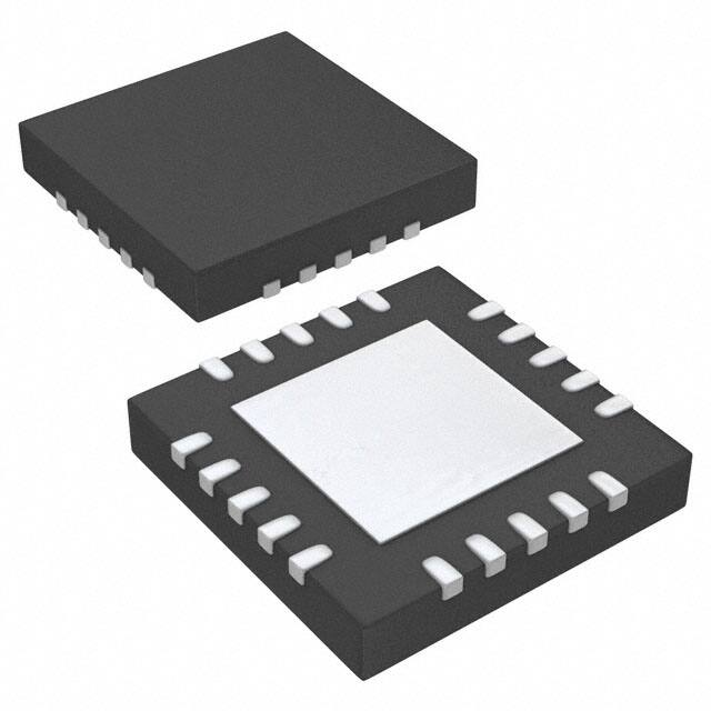


 工商网监
湘ICP备2023018690号
工商网监
湘ICP备2023018690号
