Order
Now
Product
Folder
Support &
Community
Tools &
Software
Technical
Documents
TPS92613-Q1
SLVSEC4B – APRIL 2019 – REVISED JANUARY 2020
TPS92613-Q1 Automotive Single-Channel LED Driver
1 Features
2 Applications
•
•
•
1
•
•
•
•
•
•
•
•
AEC-Q100-qualified for automotive applications:
– Temperature grade 1: –40°C to +125°C, TA
Functional safety capable
– Documentation available to aid functional
safety system design
Wide input voltage range: 4.5 V to 40 V
Low quiescent and low fault-mode current: typical
200 µA
Single high-precision current regulation:
– ±4.6% Accuracy over full junction temperature
range
– Constant current adjustable by external sense
resistor
– Up to 600 mA maximum current
– Brightness control by input PWM duty cycle
Heat sharing with external resistor
Low dropout voltage (sense-resistor voltage drop
included):
– Maximum dropout: 150 mV at 10 mA
– Maximum dropout: 400 mV at 70 mA
– Maximum dropout: 700 mV at 150 mA
– Maximum dropout: 1.3 V at 300 mA
Diagnostics and protection:
– LED open-circuit and short-circuit detection
with auto-recovery
– Diagnostic enable with adjustable threshold for
low-dropout operation
– Fault bus up to 15 devices, configurable as
either one-fails–all-fail or only-failed-channeloff (N-1)
– Thermal shutdown
Operating junction temperature range: –40°C to
+150°C
Interior lighting: dome light, reading lamp
Exterior lighting - small light: door handle, blindspot detection indicator, charging inlet
Exterior lighting - rear light: rear lamp, center highmounted stop lamp, side marker
General-purpose LED driver applications
•
•
3 Description
With LEDs being widely used in automotive
applications, simple LED drivers are more and more
popular. Comparing to discrete solutions, a low-cost
monolithic solution lowers system-level component
count and significantly improves current accuracy and
reliability.
The TPS92613-Q1 device is a single-channel, highside LED driver operating from an automotive car
battery. It is a simple, yet elegant, solution to deliver
constant current for a single LED string with full LED
diagnostics. The one-fails–all-fail feature is able to
work together with other LED drivers, such as the
TPS9261x-Q1, TPS9263x-Q1, and TPS92830-Q1
devices, to address different requirements.
Device Information(1)
PART NUMBER
TPS92613-Q1
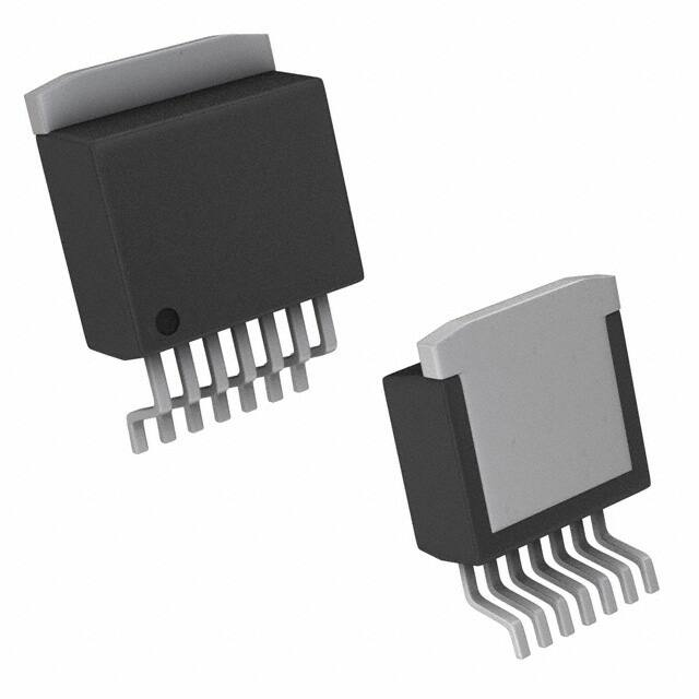
PACKAGE
TO-263 (7)
BODY SIZE (NOM)
10.16 mm × 9.85 mm
(1) For all available packages, see the orderable addendum at
the end of the data sheet.
Typical Application Diagram
4.5 V to 40 V
TPS92613 ± Q1
C(SUPPLY)
SUPPLY
R(SNS)
DIAGEN
PWM
FAULT
DIAGEN
IN
PWM
OUT
FAULT
GND
C(OUT)
1
An IMPORTANT NOTICE at the end of this data sheet addresses availability, warranty, changes, use in safety-critical applications,
intellectual property matters and other important disclaimers. PRODUCTION DATA.
�TPS92613-Q1
SLVSEC4B – APRIL 2019 – REVISED JANUARY 2020
www.ti.com
Table of Contents
1
2
3
4
5
6
7
Features ..................................................................
Applications ...........................................................
Description .............................................................
Revision History.....................................................
Pin Configuration and Functions .........................
Specifications.........................................................
1
1
1
2
3
4
6.1
6.2
6.3
6.4
6.5
6.6
6.7
4
4
4
4
4
5
7
Absolute Maximum Ratings ......................................
ESD Ratings..............................................................
Recommended Operating Conditions.......................
Thermal Information ..................................................
Electrical Characteristics...........................................
Timing Requirements ................................................
Typical Characteristics ..............................................
Detailed Description ............................................ 10
7.1 Overview ................................................................. 10
7.2 Functional Block Diagram ....................................... 10
7.3 Feature Description................................................. 10
7.4 Device Functional Modes........................................ 15
8
Application and Implementation ........................ 16
8.1 Application Information............................................ 16
8.2 Typical Applications ................................................ 16
9 Power Supply Recommendations...................... 23
10 Layout................................................................... 23
10.1 Layout Guidelines ................................................. 23
10.2 Layout Example .................................................... 23
11 Device and Documentation Support ................. 24
11.1
11.2
11.3
11.4
11.5
11.6
Documentation Support .......................................
Receiving Notification of Documentation Updates
Support Resources ...............................................
Trademarks ...........................................................
Electrostatic Discharge Caution ............................
Glossary ................................................................
24
24
24
24
24
24
12 Mechanical, Packaging, and Orderable
Information ........................................................... 24
4 Revision History
Changes from Revision A (December 2019) to Revision B
•
Added the functional safety capable link to the Features section .......................................................................................... 1
Changes from Original (April 2019) to Revision A
•
2
Page
Page
Changed data sheet status from: Advanced Information to: Production Data ...................................................................... 1
Submit Documentation Feedback
Copyright © 2019–2020, Texas Instruments Incorporated
Product Folder Links: TPS92613-Q1
�TPS92613-Q1
www.ti.com
SLVSEC4B – APRIL 2019 – REVISED JANUARY 2020
5 Pin Configuration and Functions
NDR Package
7-Pin TO-263 With Exposed Thermal Pad
Top View
5
6
OUT
IN
7
4
GND
SUPPLY
3
2
PWM
FAULT
1
DIAGEN
Thermal
Pad
Pin Functions
PIN
NO.
NAME
I/O
DESCRIPTION
1
DIAGEN
I
Enable pin for LED open-circuit detection to avoid false open diagnostics during lowdropout operation
2
PWM
I
PWM input for current output ON/OFF control
3
FAULT
I/O
Fault output, support one-fails–all-fail fault bus
4
GND
—
Ground
5
OUT
O
Constant-current output, connect to anode of the top LED in LED-string
6
IN
I
Current input
7
SUPPLY
I
Device supply voltage
—
Thermal pad
—
Thermal pad, connect to ground
Submit Documentation Feedback
Copyright © 2019–2020, Texas Instruments Incorporated
Product Folder Links: TPS92613-Q1
3
�TPS92613-Q1
SLVSEC4B – APRIL 2019 – REVISED JANUARY 2020
www.ti.com
6 Specifications
6.1 Absolute Maximum Ratings
over operating ambient temperature range (unless otherwise noted) (1)
MIN
MAX
High-voltage input
DIAGEN, IN, PWM, SUPPLY
–0.3
45
V
High-voltage output
OUT
–0.3
45
V
Fault bus
FAULT
–0.3
22
V
IN to OUT
V(IN) – V(OUT)
–0.3
45
V
SUPPLY to IN
V(SUPPLY) – V(IN)
–0.3
1
V
Operating junction temperature, TJ
–40
150
°C
Storage temperature, Tstg
–40
150
°C
(1)
UNIT
Stresses beyond those listed under Absolute Maximum Ratings may cause permanent damage to the device. These are stress ratings
only, which do not imply functional operation of the device at these or any other conditions beyond those indicated under Recommended
Operating Conditions. Exposure to absolute-maximum-rated conditions for extended periods may affect device reliability.
6.2 ESD Ratings
VALUE
Human-body model (HBM), per AEC Q100-002 (1)
Device HBM ESD Classification Level H2
V(ESD)
(1)
Electrostatic discharge
Charged-device model (CDM), per AEC Q100-011
Device CDM ESD Classification Level C3B
All pins
±2000
All pins
±500
Corner pins (1 and 7)
±750
UNIT
V
AEC Q100-002 indicates that HBM stressing shall be in accordance with the ANSI/ESDA/JEDEC JS-001 specification.
6.3 Recommended Operating Conditions
over operating ambient temperature range (unless otherwise noted)
MIN
NOM
MAX
UNIT
SUPPLY
Device supply voltage
4.5
40
V
IN
Sense voltage
4.4
40
V
PWM
PWM inputs
0
40
V
DIAGEN
Diagnostics enable pin
0
40
V
OUT
Driver output
0
40
V
FAULT
Fault bus
0
7
V
–40
125
°C
Operating ambient temperature, TA
6.4 Thermal Information
TPS92613-Q1
THERMAL METRIC (1)
NDR (TO-263)
UNIT
7 PINS
RθJA
Junction-to-ambient thermal resistance
28.4
°C/W
RθJC(top)
Junction-to-case (top) thermal resistance
23.1
°C/W
RθJB
Junction-to-board thermal resistance
10.1
°C/W
ψJT
Junction-to-top characterization parameter
4.2
°C/W
ψJB
Junction-to-board characterization parameter
9.9
°C/W
RθJC(bot)
Junction-to-case (bottom) thermal resistance
3.5
°C/W
(1)
For more information about traditional and new thermal metrics, see the Semiconductor and IC Package Thermal Metrics application
report.
6.5 Electrical Characteristics
V(SUPPLY) = 5 V to 40 V, TJ = –40°C to +150°C unless otherwise noted
PARAMETER
TEST CONDITIONS
MIN
TYP
MAX
3.2
4
UNIT
BIAS
V(POR_rising)
4
Supply voltage POR rising threshold
Submit Documentation Feedback
V
Copyright © 2019–2020, Texas Instruments Incorporated
Product Folder Links: TPS92613-Q1
�TPS92613-Q1
www.ti.com
SLVSEC4B – APRIL 2019 – REVISED JANUARY 2020
Electrical Characteristics (continued)
V(SUPPLY) = 5 V to 40 V, TJ = –40°C to +150°C unless otherwise noted
PARAMETER
TEST CONDITIONS
V(POR_falling)
Supply voltage POR falling threshold
I(Quiescent)
Device standby current
I(FAULT)
Device current in fault mode
MIN
TYP
2.2
3
MAX
UNIT
PWM = HIGH
0.1
0.2
0.25
mA
PWM = HIGH, FAULT externally pulled LOW
0.1
0.2
0.25
mA
V
LOGIC INPUTS (DIAGEN, PWM)
VIL(DIAGEN)
Input logic-low voltage, DIAGEN
1.045
1.1
1.155
V
VIH(DIAGEN)
Input logic-high voltage, DIAGEN
1.16
1.2
1.24
V
VIL(PWM)
Input logic-low voltage, PWM
1.045
1.1
1.155
V
VIH(PWM)
Input logic-high voltage, PWM
1.16
1.2
1.24
V
600
mA
CONSTANT-CURRENT DRIVER
I(OUT)
Device output-current range
V(CS_REG)
Sense-resistor regulation voltage
R(CS_REG)
Sense-resistor range
V(DROPOUT)
100% duty cycle
4
TA = 25°C, V(SUPPLY) = 4.5 V to 18 V
94
98
102
93.5
98
102.5
V(CS_REG) voltage included, current setting of 10 mA
120
150
V(CS_REG) voltage included, current setting of 70 mA
250
400
V(CS_REG) voltage included, current setting of 150
mA
430
700
V(CS_REG) voltage included, current setting of 300
mA
800
1300
TA = –40°C to +125°C, V(SUPPLY) = 4.5 V to 18 V
0.16
Voltage dropout from SUPPLY to OUT
50
mV
Ω
mV
DIAGNOSTICS
V(OPEN_th_rising)
LED open rising threshold, V(IN) – V(OUT)
235
290
335
mV
V(OPEN_th_falling)
LED open falling threshold, V(IN) – V(OUT)
70
100
135
mV
V(SG_th_rising)
Channel output V(OUT) short-to-ground
rising threshold
1.14
1.2
1.26
V
V(SG_th_falling)
Channel output V(OUT) short-to-ground
falling threshold
0.82
0.865
0.91
V
I(Retry)
Channel output V(OUT) short-to-ground
retry current
0.64
1.08
1.528
mA
FAULT
VIL(FAULT)
Logic input low threshold
VIH(FAULT)
Logic input high threshold
0.7
VOL(FAULT)
Logic output low threshold
With 500-µA external pullup
VOH(FAULT)
Logic output high threshold
With 1-µA external pulldown, V(SUPPLY) = 12 V
I(FAULT_pulldown)
FAULT internal pulldown current
I(FAULT_pullup)
FAULT internal pullup current
2
V
V
5
0.4
V
7
V
500
750
1000
µA
5
8
12
µA
157
172
187
°C
THERMAL PROTECTION
T(TSD)
Thermal shutdown junction temperature
threshold
T(TSD_HYS)
Thermal shutdown junction temperature
hysteresis
15
°C
6.6 Timing Requirements
MIN
NOM
MAX
t(PWM_delay_rising)
PWM rising edge delay, 50% PWM voltage to 10% of output current closed loop, t2 - t1 as shown
in Figure 1
10
17
25
µs
t(PWM_delay_falling)
PWM falling edge delay, 50% PWM voltage to 90% of output current open loop, t5 - t4 as shown
in Figure 1
15
21
30
µs
t(DEVICE_STARTUP)
SUPPLY rising edge to 10% output current at 200-mA set current and 14 V, t8 - t7 as shown
in Figure 1
100
150
µs
t(OPEN_deg)
LED-open fault-deglitch time
80
125
175
µs
t(SG_deg)
Output short-to-ground detection deglitch time
80
125
175
µs
t(TSD_deg)
Thermal over temperature deglitch timer
t(Recover_deg)
Fault recovery deglitch timer
50
8.5
16
µs
25
Submit Documentation Feedback
Copyright © 2019–2020, Texas Instruments Incorporated
Product Folder Links: TPS92613-Q1
UNIT
µs
5
�TPS92613-Q1
SLVSEC4B – APRIL 2019 – REVISED JANUARY 2020
www.ti.com
SUPPLY
Input duty-cycle
PWM
90%
90%
IOUT
Output duty-cycle
10%
t1
10%
10%
t2
t3
t4
t5
t6
t8
t7
Figure 1. Output Timing Diagram
6
Submit Documentation Feedback
Copyright © 2019–2020, Texas Instruments Incorporated
Product Folder Links: TPS92613-Q1
�TPS92613-Q1
www.ti.com
SLVSEC4B – APRIL 2019 – REVISED JANUARY 2020
6.7 Typical Characteristics
500
500
I(OUT) setting = 300 mA
I(OUT) setting = 150 mA
450
400
Current Output (mA)
400
Current Output (mA)
I(OUT) setting = 300 mA
I(OUT) setting = 150 mA
450
350
300
250
200
150
350
300
250
200
150
100
100
50
50
0
-40
0
8
12
16
Supply Voltage (V)
20
24
Figure 2. Output Current vs Supply Voltage
0
20
40
60
80
Temperature (oC)
100
120
140
D002
Figure 3. Output Current vs Temperature
500
250
I(OUT) setting = 300 mA
I(OUT) setting = 200 mA
I(OUT) setting = 150 mA
450
I(OUT) setting = 150 mA -40oC
I(OUT) setting = 150 mA 25oC
I(OUT) setting = 150 mA 125oC
200
Current Output (mA)
400
Current Output (mA)
-20
D001
350
300
250
200
150
100
150
100
50
50
0
0
0
0.5
1
1.5
Dropout Voltage (V)
2
2.5
0
Figure 4. Output Current vs Dropout Voltage
Output Current Duty Cycle (%)
Current Output (mA)
350
300
250
200
150
100
50
0
0
0.5
1
1.5
Dropout Voltage (V)
2
2.5
D004
2.5
10%
1%
0.5%
1%
D005
Figure 6. Output Current vs Dropout Voltage
2
100%
I(OUT) setting = 300 mA -40oC
I(OUT) setting = 300 mA 25oC
I(OUT) setting = 300 mA 125oC
400
1
1.5
Dropout Voltage (V)
Figure 5. Output Current vs Dropout Voltage
500
450
0.5
D003
10%
PWM Duty Cycle (%)
100%
D006
Figure 7. PWM Output Duty Cycle vs Input Duty Cycle
Submit Documentation Feedback
Copyright © 2019–2020, Texas Instruments Incorporated
Product Folder Links: TPS92613-Q1
7
�TPS92613-Q1
SLVSEC4B – APRIL 2019 – REVISED JANUARY 2020
www.ti.com
Typical Characteristics (continued)
Ch. 1 = V(SUPPLY)
ƒ(PWM) = 200 Hz
Ch. 3 = V(PWM)
Duty cycle = 50%
Ch. 4 = I(OUT)
Ch. 1 = V(SUPPLY)
ƒ(PWM) = 2 kHz
Figure 8. PWM Dimming at 200 Hz
Ch. 1 = V(SUPPLY)
Ch. 2 = FAULT
Ch. 4 = I(OUT)
f(PWM) = 1000 Hz
SUPPLY dimming between 2.5 V and 12 V
Ch. 3 = V(OUT)
Duty cycle = 30%
FAULT floating
Ch. 2 = V(OUT)
Ch. 3 = FAULT
Ch. 1 = SUPPLY
Ch. 4 = I(OUT)
Ch. 2 = V(OUT)
Ch. 3 = FAULT
Figure 11. Transient Undervoltage
Ch. 1 = SUPPLY
Ch. 4 = I(OUT)
Figure 12. Transient Overvoltage
8
Ch. 4 = I(OUT)
Figure 9. PWM Dimming at 2 kHz
Figure 10. Supply Dimming at 1 kHz
Ch. 1 = SUPPLY
Ch. 4 = I(OUT)
Ch. 3 = V(PWM)
Duty cycle = 50%
Submit Documentation Feedback
Ch. 2 = V(OUT)
Ch. 3 = FAULT
Figure 13. Jump Start
Copyright © 2019–2020, Texas Instruments Incorporated
Product Folder Links: TPS92613-Q1
�TPS92613-Q1
www.ti.com
SLVSEC4B – APRIL 2019 – REVISED JANUARY 2020
Typical Characteristics (continued)
Ch. 1 = SUPPLY
Ch. 4 = I(OUT)
Ch. 2 = V(OUT)
Ch. 3 = FAULT
Figure 14. Superimposed Alternating Voltage, 15 Hz
Ch. 1 = SUPPLY
Ch. 4 = I(OUT)
Ch. 2 = V(OUT)
Ch. 3 = FAULT
Figure 16. Slow Decrease and Quick Increase of Supply
Voltage
Ch. 1 = V(OUT)
Ch. 2 = FAULT
Ch. 4 = I(OUT)
Figure 18. LED Open-Circuit Protection and Recovery
Ch. 1 = SUPPLY
Ch. 4 = I(OUT)
Ch. 2 = V(OUT)
Ch. 3 = FAULT
Figure 15. Superimposed Alternating Voltage, 1 kHz
Ch. 1 = SUPPLY
Ch. 4 = I(OUT)
Ch. 2 = V(OUT)
Ch. 3 = FAULT
Figure 17. Slow Decrease and Slow Increase of Supply
Voltage
Ch. 1 = V(OUT)
Ch. 2 = FAULT
Ch. 4 = I(OUT)
Figure 19. LED Short-Circuit Protection and Recovery
Submit Documentation Feedback
Copyright © 2019–2020, Texas Instruments Incorporated
Product Folder Links: TPS92613-Q1
9
�TPS92613-Q1
SLVSEC4B – APRIL 2019 – REVISED JANUARY 2020
www.ti.com
7 Detailed Description
7.1 Overview
The TPS92613-Q1 is one device of single-channel linear LED driver family including TPS92610-Q1, TPS92611Q1 and TPS92612-Q1. The family provides a simple solution for automotive LED applications. Different package
options in the family provide variable current ranges and diagnostic options. The TPS92613-Q1 device in a TO263 package supports both LED open-circuit detection and short-to-ground detection. The TPS92613-Q1 can be
used with other TPS9261x-Q1, TPS9263x-Q1 and TPS92830-Q1 family devices together to realize one-fails-allfail protection by tying all FAULT pins together as a fault bus.
The current output at OUT pin can be set by an external R(SNS) resistor. Current flows from the supply through
the R(SNS) resistor into the integrated current regulation circuit and to the LEDs through OUT pin.
7.2 Functional Block Diagram
4.5 ± 40V
TPS92613-Q1
R(SNS)
IN
±
+
SUPPLY
DIAGEN
PWM
Supply
and
Control
Output Driver
OUT
FAULT
LED Diagnostics
GND
7.3 Feature Description
7.3.1 Power Supply
7.3.1.1 Power-On Reset (POR)
The TPS92613-Q1 device has an internal power-on-reset (POR) function. When power is applied to the SUPPLY
pin, the internal POR circuit holds the device in reset state until V(SUPPLY) is above V(POR_rising).
7.3.1.2 Low-Quiescent-Current
The TPS92613-Q1 device consumes minimal quiescent current, less than 250 µA into SUPPLY when the FAULT
pin is externally pulled LOW. At the same time, the device shuts down the output driver.
If device detects an internal fault, it pulls down the FAULT pin by an internal typical 750-µA constant current as a
fault indication to the fault bus.
10
Submit Documentation Feedback
Copyright © 2019–2020, Texas Instruments Incorporated
Product Folder Links: TPS92613-Q1
�TPS92613-Q1
www.ti.com
SLVSEC4B – APRIL 2019 – REVISED JANUARY 2020
Feature Description (continued)
7.3.2 Constant-Current Driver
The TPS92613-Q1 device is a high-side current driver for driving LEDs. The device controls the output current
through regulating the voltage drop on an external high-side current-sense resistor, R(SNS). An integrated error
amplifier drives an internal power transistor to maintain the voltage drop on the current-sense resistor R(SNS) to
V(CS_REG) and therefore regulates the current output to target value. When the output current is in regulation, the
current value can be calculated by using Equation 1.
V(CS _ REG)
I(OUT)
R(SNS)
where
•
V(CS_REG) = 98 mV (typical)
(1)
When the supply voltage drops below total LED string forward voltage plus required dropout voltage, V(DROPOUT),
the TPS92613-Q1 is not able to deliver enough current output as set by the value of R(SNS), and the voltage
across the current-sense resistor R(SNS) is less than V(CS_REG).
7.3.3 PWM Control
The pulse width modulation (PWM) input of the TPS92613-Q1 functions as enable for the output current. When
the voltage applied on the PWM pin is higher than VIH(PWM), the output current is enabled. When the voltage
applied on PWM pin is lower than VIL(PWM), the output current is disabled as well as the diagnostic features.
Besides output current enable and disable function, the PWM input of TPS92613-Q1 also supports adjustment of
the average current output for brightness control if the frequency of applied PWM signal is higher than 100 Hz,
which is out of visible frequency range of human eyes. TI recommends a 200-Hz PWM signal with 1% to 100%
duty cycle input for brightness control. See to Figure 20 for typical PWM dimming application.
4.5 ± 40V
TPS92613 ± Q1
C(SUPPLY)
SUPPLY
R(SNS)
DIAGEN
PWM
1%~100%@200Hz
FAULT
DIAGEN
IN
PWM
OUT
FAULT
GND
C(OUT)
Figure 20. Typical Application Schematic for PWM Dimming
7.3.4 Supply Control
The TPS92613-Q1 supports supply control to turn ON and OFF output current. When the voltage applied on the
SUPPLY pin is higher than the LED string forward voltage plus needed V(DROPOUT) at required current, and the
PWM pin voltage is high, the output current is turned ON and well regulated. However, if the voltage applied on
the SUPPLY pin is lower than V(POR_falling), the output current is turned OFF. With this feature, the power-supply
voltage in the designed pattern controls the output current ON/OFF. The brightness can be adjustable if the
ON/OFF frequency is fast enough. Because of the high accuracy design of PWM threshold in TPS92613-Q1, TI
recommends a resistor divider on the PWM pin to set the SUPPLY threshold higher than LED forward voltage
plus V(DROPOUT) as shown in Figure 21. When the voltage on the PWM pin is higher than VIH(PWM), the output
current is turned ON. However, when the voltage on the PWM is lower than VIL(PWM), the output current is turned
OFF.
Submit Documentation Feedback
Copyright © 2019–2020, Texas Instruments Incorporated
Product Folder Links: TPS92613-Q1
11
�TPS92613-Q1
SLVSEC4B – APRIL 2019 – REVISED JANUARY 2020
www.ti.com
Feature Description (continued)
TPS92613 ± Q1
C(SUPPLY)
SUPPLY
R(SNS)
DIAGEN
PWM
FAULT
DIAGEN
IN
PWM
OUT
FAULT
GND
C(OUT)
Figure 21. Typical Application Schematic for SUPPLY Control
7.3.5 Diagnostics and Protection
The TPS92613-Q1 device provides advanced diagnostics and fault-protection features for automotive exterior
lighting systems. The device is able to detect and protect fault from LED-string short-to-GND, LED-string opencircuit and junction overtemperature scenarios. It also supports a one-fails–all-fail fault bus design that can
flexibly fit different regulatory requirements.
7.3.5.1 Open-Circuit Detection
The TPS92613-Q1 device has LED open-circuit detection. The LED open-circuit detection monitors the output
voltage when the current output is enabled. The LED open-circuit detection is only enabled when DIAGEN is
HIGH. A short-to-battery fault is also detected and recognized as an LED open-circuit fault.
The TPS92613-Q1 monitors dropout-voltage differences between the IN and OUT pins when PWM is HIGH. The
voltage difference V(IN) – V(OUT) is compared with the internal reference voltage V(OPEN_th_falling) to detect an LED
open-circuit incident. If V(IN) – V(OUT) falls below the V(OPEN_th_falling) voltage longer than the deglitch time of
t(OPEN_deg), the device asserts an open-circuit fault. Once an LED open-circuit failure is detected, the internal
constant-current sink pulls down the FAULT pin voltage. During the deglitch time period, if V(IN) – V(OUT) rises
above V(OPEN_th_rising), the deglitch timer is reset.
The TPS92613-Q1 keeps the current output enabled to retry after LED open-circuit fault is detected if the PWM
input is HIGH; the device sources a small current I(retry) from IN to OUT when PWM input is LOW. In either
scenario, once the fault condition is removed, the device resumes normal operation and releases the FAULT pin.
7.3.5.2 Short-to-GND Detection
The TPS92613-Q1 device has LED short-to-GND detection. The LED short-to-GND detection monitors the
output voltage when the output current is enabled. Once a short-to-GND LED failure is detected, the device turns
off the output channel and retries automatically, regardless of the state of the PWM input. If the retry mechanism
detects the removal of the LED short-to-GND fault, the device resumes to normal operation.
The TPS92613-Q1 monitors the V(OUT) voltage and compares it with the internal reference voltage to detect a
short-to-GND failure. If V(OUT) falls below V(SG_th_falling) longer than the deglitch time of t(SG_deg), the device asserts
the short-to-GND fault and pulls low the FAULT pin. During the deglitching time period, if V(OUT) rises above
V(SG_th_rising), the timer is reset.
Once the TPS92613-Q1 has asserted a short-to-GND fault, the device turns off the output channel and retries
automatically with a small current. During retrying the device sources a small current I(retry) from IN to OUT to pull
up the LED loads continuously. Once auto-retry detects output voltage rising above V(SG_th_falling), it clears the
short-to-GND fault and resumes to normal operation.
12
Submit Documentation Feedback
Copyright © 2019–2020, Texas Instruments Incorporated
Product Folder Links: TPS92613-Q1
�TPS92613-Q1
www.ti.com
SLVSEC4B – APRIL 2019 – REVISED JANUARY 2020
Feature Description (continued)
7.3.5.3 Overtemperature Protection
The TPS92613-Q1 device monitors device junction temperature. When the junction temperature reaches thermal
shutdown threshold T(TSD), the output shuts down. Once the junction temperature falls below T(TSD) – T(TSD_HYS),
the device recovers to normal operation. During overtemperature protection, the FAULT pin is pulled low.
7.3.5.4 DIAGEN
The TPS92613-Q1 device supports the DIAGEN pin with an accurate threshold to disable the LED open-circuit
diagnostic functions. The DIAGEN pin can be used to enable or disable LED open-circuit protection based on
SUPPLY pin voltage sensed by an external resistor divider. When the voltage applied on DIAGEN pin is higher
than the threshold VIH(DIAGEN), the device enables LED open-circuit diagnosis. When V(DIAGEN) is lower than the
threshold VIL(DIAGEN), the device disables LED-open-circuit detection.
Only LED open-circuit detection can be disabled by pulling down the DIAGEN pin. The LED short-to-GND
detection and overtemperature protection cannot be turned off by pulling down the DIAGEN pin.
7.3.5.5 Low-Dropout Operation
When the supply voltage drops below LED string total forward voltage plus V(DROPOUT) at required current, the
TPS92613-Q1 device operates in low-dropout conditions to deliver current output as close as possible to target
value. The actual current output is less than preset value due to insufficient headroom voltage for power
transistor. As a result, the voltage across the sense resistor fails to reach the regulation target.
If the TPS92613-Q1 is designed to operate in low-dropout condition, and the open-circuit diagnostics must be
disabled by pulling the DIAGEN pin voltage lower than VIL(DIAGEN). Otherwise, the TPS92613-Q1 detects an
open-circuit fault and reports a fault indication on the FAULT pin. The DIAGEN pin is used to avoid false
diagnostics due to low supply voltage.
In low-dropout operation, a diode in parallel with the sense resistor is recommended to clamp the voltage
between SUPPLY and IN (across the sense resistor) in case of a large current pulse during recovery.
7.3.6 FAULT Bus Output With One-Fails–All-Fail
During normal operation, The FAULT pin of TPS92613-Q1 is weakly pulled up by an internal pullup current
source, I(FAULT_pullup) higher than VOH(FAULT). If any fault scenario occurs, the FAULT pin is strongly pulled low by
the internal pulldown current sink, I(FAULT_pulldown) to report out the fault alarm.
Meanwhile, the TPS92613-Q1 also monitors the FAULT pin voltage internally. If the FAULT pin of the
TPS92613-Q1 is pulled low by external current sink below VIL(FAULT), the current output is turned off even though
there is no fault detected on owned output. The device does not resume to normal operation until the FAULT pin
voltage rises above VIH(FAULT).
4.5 ± 40V
TPS92613 ± Q1
A
SUPPLY
TPS92613 ± Q1
B
C(SUPPLY)
C(SUPPLY)
SUPPLY
R(SNS)
R(SNS)
DIAGEN
PWM
FAULT
DIAGEN
DIAGEN
IN
PWM
OUT
FAULT
GND
PWM
FAULT
C(OUT)
DIAGEN
IN
PWM
OUT
FAULT
GND
C(OUT)
FAULT
BUS
Figure 22. Typical Application Schematic for One-Fails-All-Fail
Submit Documentation Feedback
Copyright © 2019–2020, Texas Instruments Incorporated
Product Folder Links: TPS92613-Q1
13
�TPS92613-Q1
SLVSEC4B – APRIL 2019 – REVISED JANUARY 2020
www.ti.com
Feature Description (continued)
Based on this feature, the TPS92613-Q1 device is able to construct a FAULT bus by tying FAULT pins from
multiple TPS9261x-Q1, TPS9263x-Q1 or TPS92830-Q1 devices to realize one-fails-all-fail function as Figure 22
showing. The right side TPS92613-Q1 (B) detects either LED open-circuit fault or LED short-to-GND fault and
pulls low the FAULT pin. The low voltage on FAULT pin is detected by left side TPS92613-Q1 (A) because the
FAULT pins are connected of two devices. The left TPS92613-Q1 (A) turns off the output current as a result.
If the FAULT pin is externally pulled up with a current larger than I(FAULT_pulldown), the one-fails–all-fail function is
disabled and only the faulty channel is turned off.
The FAULT bus is able to support up to 15 pieces of TPS9261x-Q1, TPS9263x-Q1, or TPS92830-Q1 devices.
7.3.7 Fault Table
Table 1. Fault Table With DIAGEN = HIGH
FAULT BUS
STATUS
FAULT TYPE
DETECTION
MECHANISM
Open-circuit or
short-to-supply
V(IN) – V(OUT) <
V(OPEN_th_falling)
Short-to-ground
V(OUT) <
V(SG_th_falling)
Overtemperature
TJ > T(TSD)
FAULT floating
or externally
pulled up
CURRENT
OUTPUT
DEGLITCH
TIME
FAULT BUS
FAULT HANDLING
ROUTINE
FAULT
RECOVERY
Auto recovery
t(OPEN_deg)
Constantcurrent
pulldown
Device works normally
with FAULT pin pulled
low. Device sources
I(retry) current when
PWM is LOW. Device
keeps output normal
when PWM is HIGH.
On
t(SG_deg)
Constantcurrent
pulldown
Device turns output off
and retries with
Auto recovery
constant current I(retry),
ignoring the PWM input.
On or off
t(TSD_deg)
Constantcurrent
pulldown
Device turns output off.
On
Externally
pulled low
Auto recovery
Device turns output off
Table 2. Fault Table With DIAGEN = LOW
FAULT BUS
STATUS
FAULT TYPE
DETECTION
MECHANISM
CURRENT
OUTPUT
DEGLITCH
TIME
Open-circuit or
short-to-supply
FAULT floating
or externally
pulled up
FAULT HANDLING
ROUTINE
FAULT
RECOVERY
Ignored
Short-to-ground
VOUT <
V(SG_th_falling)
On
t(SG_deg)
Constantcurrent
pulldown
Device turns output off
and retries with
Auto recovery
constant current I(retry),
ignoring the PWM input.
Overtemperature
TJ > T(TSD)
On or off
t(TSD_deg)
Constantcurrent
pulldown
Device turns output off.
Externally
pulled low
14
FAULT BUS
Auto recovery
Device turns output off
Submit Documentation Feedback
Copyright © 2019–2020, Texas Instruments Incorporated
Product Folder Links: TPS92613-Q1
�TPS92613-Q1
www.ti.com
SLVSEC4B – APRIL 2019 – REVISED JANUARY 2020
7.4 Device Functional Modes
7.4.1 Undervoltage Lockout, V(SUPPLY) < V(POR_rising)
When the device is in undervoltage lockout status, the TPS92613-Q1 device disables all functions until the
supply rises above the V(POR_rising) threshold.
7.4.2 Normal Operation V(SUPPLY) ≥ 4.5 V
The device drives an LED string in normal operation. With enough voltage drop across SUPPLY and OUT, the
device is able to drive the output in constant-current mode.
7.4.3 Low-Voltage Dropout Operation
When the device drives an LED string in low-dropout operation, if the voltage drop is less than the open-circuit
detection threshold, the device may report a false open-circuit fault. TI recommends only enabling the opencircuit detection when SUPPLY voltage is enough higher than LED string voltage to avoid a false open-circuit
detection.
7.4.4 Fault Mode
When the device detects an open circuit or a shorted LED, the device tries to pull down the FAULT pin with a
constant current. If the FAULT bus is pulled down, the device switches to fault mode and consumes a fault
current of I(FAULT).
Submit Documentation Feedback
Copyright © 2019–2020, Texas Instruments Incorporated
Product Folder Links: TPS92613-Q1
15
�TPS92613-Q1
SLVSEC4B – APRIL 2019 – REVISED JANUARY 2020
www.ti.com
8 Application and Implementation
NOTE
Information in the following applications sections is not part of the TI component
specification, and TI does not warrant its accuracy or completeness. TI’s customers are
responsible for determining suitability of components for their purposes. Customers should
validate and test their design implementation to confirm system functionality.
8.1 Application Information
In automotive lighting applications, thermal performance and LED diagnostics are always design challenges for
linear LED drivers.
The TPS92613-Q1 device is capable of detecting LED open-circuit and LED short-circuits. To increase currentdriving capability, the TPS92613-Q1 device supports using an external parallel resistor to help dissipate heat as
following section Single-Channel LED Driver With Heat Sharing describes. This method provides a low-cost
solution of using external resistors to minimize thermal accumulation on the device itself due to large voltage
difference between input voltage and LED string forward voltage, while still keeping high accuracy of the total
current output. Note that the one-fails–all-fail feature is not supported by this topology.
8.2 Typical Applications
8.2.1 Single-Channel LED Driver With Diagnostics
The TPS92613-Q1 is an easy-to-use solution for LED driver applications with diagnostics requirements.
9 ± 16V
TPS92613 ± Q1
C(SUPPLY)
SUPPLY
R2
R(SNS)
DIAGEN
R1
PWM
FAULT
DIAGEN
IN
PWM
OUT
FAULT
GND
C(OUT)
Figure 23. Typical Application Diagram
8.2.1.1 Design Requirements
Input voltage range is from 9 V to 16 V, LED maximum forward voltage VF_MAX = 2.5 V, minimum forward voltage
VF_MIN = 1.9 V, current I(LED) = 250 mA. PWM input is adopted for LED brightness adjust and LED ON/OFF
control.
8.2.1.2 Detailed Design Procedure
STEP 1: Determine the current setting resistor, R(SNS) value by using Equation 2.
V(CS _ REG)
R(SNS)
0.392:
I(LED)
where
•
•
16
V(CS_REG) = 98 mV (typical.)
I(LED) = 250 mA
(2)
Submit Documentation Feedback
Copyright © 2019–2020, Texas Instruments Incorporated
Product Folder Links: TPS92613-Q1
�TPS92613-Q1
www.ti.com
SLVSEC4B – APRIL 2019 – REVISED JANUARY 2020
Typical Applications (continued)
STEP 2: Design the threshold voltage for SUPPLY to enable the LED open-circuit diagnostics and calculate the
resistor divider value.
LED-string maximum forward voltage = 3 × 2.5 V = 7.5 V. To avoid the open-circuit fault reported in low-dropout
operation conditions, additional headroom between SUPPLY and OUT needs to be considered. The TPS92613Q1 device must disable open-circuit detection when the supply voltage is below LED-string maximum forward
voltage plus maximum V(OPEN_th_rising) and maximum V(CS_REG). The voltage divider resistor, R1 and R2 value can
be calculated by Equation 3.
VIL(DIAGEN)
V OPEN _ th _ ri sing
V(CS _ REG)
V(OUT) u R1
R1 R2
where
•
•
•
•
VIL(DIAGEN) = 1.045 V (minimum)
V(OPEN_th_rising) = 335 mV (maximum)
V(CS_REG) = 102.5 mV (maximum)
R1 = 10 kΩ recommended
(3)
The calculated result for R2 is 65.7 kΩ when V(OUT) maximum voltage is 7.5 V.
STEP 3: Thermal analysis for the worst application conditions.
Normally the thermal analysis is necessary for linear LED-driver applications to ensure that the operation junction
temperature of TPS92613-Q1 is well managed. The total power consumption on the TPS92613-Q1 itself is one
important factor determining operation junction temperature, and it can be calculated by using Equation 4. Based
on the worst-case analysis for maximum power consumption on device, consider either optimizing PCB layout for
better power dissipation as Layout describes or adding an extra heat-sharing resistor as described in SingleChannel LED Driver With Heat Sharing.
P DEV
V SUPPLY
P DEV _ MAX
V CS _ REG
V OUT u I LED
V SUPPLY u I Quiescent
16 3 u 1.9 0.098 u 0.25 16 u 0.00025
2.55W
where
•
•
V(CS_REG) = 98 mV (typical)
I(Quiescent) = 250 µA (maximum)
(4)
In this application, the calculated result for maximum power consumption on the TPS92613-Q1 is 2.55 W at
V(SUPPLY) = 16 V and I(LED) = 250 mA conditions.
TI recommends to add capacitors C(SUPPLY) at SUPPLY and C(OUT)at OUT. TI recommends one 1-μF capacitor
plus one 100-nF decoupling ceramic capacitor close to the SUPPLY pin for C(SUPPLY) and a 10-nF ceramic
capacitor close to the OUT pin for C(OUT). The larger capacitor for C(SUPPLY) or C(OUT) is helpful for EMI and ESD
immunity; however, large C(OUT) takes a longer time to charge up the capacitor and may affect PWM dimming
performance.
Submit Documentation Feedback
Copyright © 2019–2020, Texas Instruments Incorporated
Product Folder Links: TPS92613-Q1
17
�TPS92613-Q1
SLVSEC4B – APRIL 2019 – REVISED JANUARY 2020
www.ti.com
Typical Applications (continued)
8.2.1.3 Application Curves
Ch. 1 = V(OUT)
Ch. 2 = V(PWM)
Ch. 4 = I(OUT)
Ch. 1 = V(OUT)
Figure 24. Output Current With PWM Input
Ch. 2 = V(PWM)
Ch. 4 = I(OUT)
Figure 25. Output Current With PWM Input
8.2.2 Single-Channel LED Driver With Heat Sharing
Using parallel resistors, thermal performance can be improved by balancing current between the TPS92613-Q1
device and the external resistors as follows. As the current-sense resistor controls the total LED string current,
the LED string current I(LED) is set by V(CS_REG) / R(SNS), while the TPS92613-Q1 current I(DRIVE) and parallel
resistor current I(P) combine to the total current.
TPS92613 ± Q1
C(SUPPLY)
SUPPLY
R2
R1
R4
DIAGEN
R3
PWM
FAULT
R(SNS)
I(DRIVE)
DIAGEN
I(LED)
IN
R(P)
PWM
OUT
FAULT
GND
I(P)
C(OUT)
Figure 26. Supply Control With Heat Sharing Resistor
8.2.2.1 Design Requirements
Input voltage range is 9 V to 16 V, LED maximum forward voltage VF_MAX= 2.5 V, minimum forward voltage
VF_MIN = 1.9 V, current I(LED) = 500 mA. And supply control is adopted for LED brightness adjust and LED
ON/OFF control. The high level of V(SUPPLY) is 9 V to 16 V, and the low level of V(SUPPLY) is between 0 V to 3 V.
18
Submit Documentation Feedback
Copyright © 2019–2020, Texas Instruments Incorporated
Product Folder Links: TPS92613-Q1
�TPS92613-Q1
www.ti.com
SLVSEC4B – APRIL 2019 – REVISED JANUARY 2020
Typical Applications (continued)
8.2.2.2 Detailed Design Procedure
Note that the parallel resistor path cannot be shut down by PWM or fault protection. If PWM control is required,
TI recommends an application circuit as described in Figure 27.
In linear LED driver applications, the large input voltage variation generates the most of the thermal concerns.
The resistor current, as indicated by Ohm's law, depends on the voltage across the external resistors. The
TPS92613-Q1 controls the driver current I(DRIVE) to attain the desired total current. If I(P) increases, the
TPS92613-Q1 device decreases I(DRIVE) to compensate, and vice versa.
While in low-dropout operation, the voltage across the R(P) resistor may be close to zero, so that almost no
current can flow through the external resistor R(P).
When the input voltage is high, the parallel-resistor current I(P) is proportional to the voltage across the parallel
resistor R(P). The parallel resistor R(P) takes the majority of the total string current, generating maximum heat.
In this case, the parallel resistor value must be carefully calculated to ensure that 1) enough output current is
achieved in low-dropout operation, 2) thermal dissipation for both the TPS92613-Q1 device and the resistor is
within their thermal dissipation limits, and 3) device current in the high-voltage mode is above the minimal outputcurrent requirement.
STEP 1: Determine the current setting resistor, R(SNS) value by using Equation 5.
V(CS _ REG)
R(SNS)
0.196:
I(LED)
where
•
•
V(CS_REG) = 98 mV (typical)
I(LED) = 500 mA
(5)
The calculated result for R(SNS) is 0.196 Ω.
STEP 2: Calculate the parallel resistor, R(P) value by using Equation 6.
The parallel resistor R(P) is recommended to consume 50% of the total current at maximum supply voltage.
V(SUPPLY) V(CS _ REG) V(OUT) 16 0.098 3 u 1.9
R(P)
| 40:
0.5 u I(LED)
0.5 u 0.5
where
•
•
V(CS_REG) = 98 mV (typical)
I(LED) = 500 mA
(6)
The calculated result for R(P) is about 40 Ω at V(SUPPLY) = 16 V.
STEP 3: Design the threshold voltage for SUPPLY to enable the LED open-circuit diagnostics and calculate
voltage divider resistor value for R1 and R2.
LED-string maximum forward voltage = 3 × 2.5 V = 7.5 V. To avoid the open-circuit fault reported in low-dropout
operation conditions, additional headroom between SUPPLY and OUT needs to be considered. The TPS92613Q1 device must disable open-circuit detection when the supply voltage is below LED-string maximum forward
voltage plus maximum V(OPEN_th_rising) and maximum V(CS_REG). The voltage divider resistor, R1 and R2 value can
be calculated by Equation 7.
VIL(DIAGEN)
V OPEN _ th _ ri sing
V(CS _ REG)
V(OUT) u R1
R1 R2
where
•
•
•
•
VIL(DIAGEN) = 1.045 V (minimum)
V(OPEN_th_rising) = 335 mV (maximum)
V(CS_REG) = 102.5 mV (maximum)
R1 = 10 kΩ recommended
(7)
Submit Documentation Feedback
Copyright © 2019–2020, Texas Instruments Incorporated
Product Folder Links: TPS92613-Q1
19
�TPS92613-Q1
SLVSEC4B – APRIL 2019 – REVISED JANUARY 2020
www.ti.com
Typical Applications (continued)
The calculated result for R2 is 65.7 kΩ when V(OUT) maximum voltage is 7.5 V.
STEP 4: Design the threshold voltage for PWM to enable current output and calculate voltage divider resistor
value for R3 and R4.
Because the supply control is adopted for the LED ON/OFF and brightness control, a pulse square voltage with
power capability is applied on the SUPPLY pin to enable and disable current output to OUT. In order to ensure
the current output of TPS92613-Q1 is fully enabled when applied voltage on SUPPLY pin is high enough and the
current output is truly shutdown when the applied voltage goes low. A voltage divider from supply to control PWM
needs to be designed to setup a threshold of supply voltage. The resistor R3 and R4 of voltage divider can be
calculated by Equation 8.
V SUPPLY u R3
VIL(PWM)
R3 R 4
where
•
•
VIL(PWM) = 1.24 V (maximum)
R3 = 10 kΩ recommended
(8)
The calculated result for R4 is 30.5 kΩ if LED must be turned on when V(SUPPLY) voltage is higher than 5 V.
STEP 5: Thermal analysis for the worst application conditions.
The total device power consumption can be calculated by Equation 9.
P DEV
§
V SUPPLY V CS _ REG V OUT ·
¸ V
V OUT u ¨ I LED
SUPPLY u I Quiescent
RP
¨
¸
©
¹
16 0.098 3 u 1.9 ·
§
16 0.098 3 u 1.9 u ¨ 0.5
¸ 16 u 0.00025 2.50W
40
©
¹
V SUPPLY
P DEV _ MAX
V CS _ REG
where
•
•
V(CS_REG) = 98 mV (typical)
I(Quiescent) = 250 µA (maximum)
(9)
The calculated maximum power consumption on the TPS61193-Q1 is 2.5 W at V(SUPPLY) = 16 V, V(OUT) = 3 × 1.9
V = 5.7 V and I(LED) = 500 mA.
The power consumption on resistor R(P) can be calculated through Equation 10.
V(SUPPLY)
P(RP)
V(CS _ REG)
V(OUT)
2
R(P)
P(RP _ MAX)
16 3 u 1.9 0.098
40
2
2.6W
where
•
V(CS_REG) = 98 mV (Typ.)
(10)
The calculated maximum power consumption on the 40 Ω, R(P) parallel resistor is 2.6 W at V(SUPPLY) = 16 V and
V(OUT) = 3 × 1.9 V = 5.7 V.
TI recommends adding capacitors C(SUPPLY) at SUPPLY and C(OUT)at OUT. One 1-μF capacitor plus one 100-nF
decoupling ceramic capacitor close to the SUPPLY pin is recommended for C(SUPPLY), and a 10-nF ceramic
capacitor close to the OUT pin is recommended for C(OUT). The larger capacitor for C(SUPPLY) or C(OUT) is helpful
for EMI and ESD immunity, however large C(OUT) takes a longer time to charge up the capacitor and could affect
PWM dimming performance.
20
Submit Documentation Feedback
Copyright © 2019–2020, Texas Instruments Incorporated
Product Folder Links: TPS92613-Q1
�TPS92613-Q1
www.ti.com
SLVSEC4B – APRIL 2019 – REVISED JANUARY 2020
Typical Applications (continued)
9 ± 16V
TPS92613 ± Q1
C(SUPPLY)
SUPPLY
R2
DIAGEN
R1
PWM
FAULT
PWM
R(SNS)
I(DRIVE)
DIAGEN
I(LED)
IN
R(P)
PWM
OUT
FAULT
GND
PWM
I(P)
C(OUT)
R5
Figure 27. PWM Control With Heat Sharing Resistor
For PWM control scenarios, a NPN bipolar transistor with a base current-limiting resistor, R5 can modulate the
output current together with the device PWM function as Figure 27. The resistor value of R5 needs to be
calculated based on the applied PWM voltage and β value of selected NPN transistor.
Submit Documentation Feedback
Copyright © 2019–2020, Texas Instruments Incorporated
Product Folder Links: TPS92613-Q1
21
�TPS92613-Q1
SLVSEC4B – APRIL 2019 – REVISED JANUARY 2020
www.ti.com
Typical Applications (continued)
8.2.2.3 Application Curves
Ch. 1 = V(SUPPLY)
Ch. 4 = I(LED)
V(SUPPLYHI) = 12V
Ch. 2 = V(OUT)
F(SUPPLY) = 200 Hz
V(SUPPLYLO) = 2.5V
Ch. 3 = I(P)
Duty Cycle = 5%
Ch. 1 = V(SUPPLY)
Ch. 4 = I(LED)
V(SUPPLYHI) = 12V
Figure 28. Pulse Supply Control Output Current (D = 5%)
Ch. 2 = V(OUT)
F(SUPPLY) = 200 Hz
V(SUPPLYLO) = 2.5V
Ch. 3 = I(P)
Duty Cycle = 30%
Figure 29. Pulse Supply Control Output Current (D = 30%)
700
Dropout Voltage (V)
600
500
400
300
I(OUT) setting = 500 mA -40oC
I(OUT) setting = 500 mA 25oC
I(OUT) setting = 500 mA 125oC
I(OUT) setting = 600 mA -40oC
I(OUT) setting = 600 mA 25oC
I(OUT) setting = 600 mA 125oC
200
100
0
0
Ch. 1 = V(SUPPLY)
Ch. 4 = I(LED)
1
1.5
2
2.5
Current Output (mA)
3
3.5
4
D007
Ch. 2 = V(OUT)
Ch. 3 = I(P)
V(SUPPLY) increases from 9 V to 16 V
Figure 30. Constant Output Current With Supply Voltage
Increasing
22
0.5
Figure 31. Output Current vs Dropout Voltage
Submit Documentation Feedback
Copyright © 2019–2020, Texas Instruments Incorporated
Product Folder Links: TPS92613-Q1
�TPS92613-Q1
www.ti.com
SLVSEC4B – APRIL 2019 – REVISED JANUARY 2020
9 Power Supply Recommendations
The TPS92613-Q1 is designed to operate from an automobile electrical power system within the range specified
in the Recommended Operating Conditions. The V(SUPPLY) input must be protected from reverse voltage and
voltage dump condition over 40 V. The impedance of the input supply rail must be low enough that the input
current transient does not cause drop below LED string required forward voltage. If the input supply is connected
with long wires, additional bulk capacitance may be required in addition to normal input capacitor.
10 Layout
10.1 Layout Guidelines
Thermal dissipation is the primary consideration for TPS92613-Q1 layout. TI recommends large thermal
dissipation area connected to thermal pads with multiple thermal vias.
10.2 Layout Example
GND
DIAGEN
PWM
SUPPLY
IN
FAULT
GND
OUT
Figure 32. TPS92613-Q1 Example Layout Diagram
Submit Documentation Feedback
Copyright © 2019–2020, Texas Instruments Incorporated
Product Folder Links: TPS92613-Q1
23
�TPS92613-Q1
SLVSEC4B – APRIL 2019 – REVISED JANUARY 2020
www.ti.com
11 Device and Documentation Support
11.1 Documentation Support
11.1.1 Related Documentation
For related documentation see the following:
• TPS92610-Q1 Automotive Single-Channel Linear LED Driver
• TPS92611-Q1 Automotive Single-Channel Linear LED Driver
• TPS92612-Q1 Automotive Single-Channel Linear LED Driver
• TPS92610-Q1 EVM User's Guide
• How to Calculate TPS92630-Q1 Maximum Output Current for Automotive Exterior Lighting Applications
• Automotive Linear LED Driver Reference Design for Center High-mounted Stop Lamp (CHMSL) product
folder
• Automotive Linear LED Driver Reference Design for Center High-mounted Stop Lamp (CHMSL) reference
design guide
11.2 Receiving Notification of Documentation Updates
To receive notification of documentation updates, navigate to the device product folder on ti.com. In the upper
right corner, click on Alert me to register and receive a weekly digest of any product information that has
changed. For change details, review the revision history included in any revised document.
11.3 Support Resources
TI E2E™ support forums are an engineer's go-to source for fast, verified answers and design help — straight
from the experts. Search existing answers or ask your own question to get the quick design help you need.
Linked content is provided "AS IS" by the respective contributors. They do not constitute TI specifications and do
not necessarily reflect TI's views; see TI's Terms of Use.
11.4 Trademarks
E2E is a trademark of Texas Instruments.
All other trademarks are the property of their respective owners.
11.5 Electrostatic Discharge Caution
This integrated circuit can be damaged by ESD. Texas Instruments recommends that all integrated circuits be handled with
appropriate precautions. Failure to observe proper handling and installation procedures can cause damage.
ESD damage can range from subtle performance degradation to complete device failure. Precision integrated circuits may be more
susceptible to damage because very small parametric changes could cause the device not to meet its published specifications.
11.6 Glossary
SLYZ022 — TI Glossary.
This glossary lists and explains terms, acronyms, and definitions.
12 Mechanical, Packaging, and Orderable Information
The following pages include mechanical, packaging, and orderable information. This information is the mostcurrent data available for the designated device. This data is subject to change without notice and without
revision of this document. For browser-based versions of this data sheet, see the left-hand navigation pane.
24
Submit Documentation Feedback
Copyright © 2019–2020, Texas Instruments Incorporated
Product Folder Links: TPS92613-Q1
�PACKAGE OPTION ADDENDUM
www.ti.com
10-Dec-2020
PACKAGING INFORMATION
Orderable Device
Status
(1)
Package Type Package Pins Package
Drawing
Qty
Eco Plan
(2)
Lead finish/
Ball material
MSL Peak Temp
Op Temp (°C)
Device Marking
(3)
(4/5)
(6)
TPS92613QNDRRQ1
ACTIVE
TO-263
NDR
7
1000
RoHS & Green
SN
Level-3-260C-168 HR
-40 to 125
TPS92613Q
(1)
The marketing status values are defined as follows:
ACTIVE: Product device recommended for new designs.
LIFEBUY: TI has announced that the device will be discontinued, and a lifetime-buy period is in effect.
NRND: Not recommended for new designs. Device is in production to support existing customers, but TI does not recommend using this part in a new design.
PREVIEW: Device has been announced but is not in production. Samples may or may not be available.
OBSOLETE: TI has discontinued the production of the device.
(2)
RoHS: TI defines "RoHS" to mean semiconductor products that are compliant with the current EU RoHS requirements for all 10 RoHS substances, including the requirement that RoHS substance
do not exceed 0.1% by weight in homogeneous materials. Where designed to be soldered at high temperatures, "RoHS" products are suitable for use in specified lead-free processes. TI may
reference these types of products as "Pb-Free".
RoHS Exempt: TI defines "RoHS Exempt" to mean products that contain lead but are compliant with EU RoHS pursuant to a specific EU RoHS exemption.
Green: TI defines "Green" to mean the content of Chlorine (Cl) and Bromine (Br) based flame retardants meet JS709B low halogen requirements of


 工商网监
湘ICP备2023018690号
工商网监
湘ICP备2023018690号
