Order
Now
Product
Folder
Technical
Documents
Support &
Community
Tools &
Software
TPS92662A-Q1
SLUSDV6A – OCTOBER 2019 – REVISED JANUARY 2020
TPS92662A-Q1 High Brightness LED Matrix Manager with EMI Mitigation Techniques
1 Features
3 Description
•
The TPS92662A-Q1 LED matrix manager device
enables fully dynamic adaptive lighting solutions by
providing individual pixel-level LED control. The
device includes four sub-strings of three seriesconnected integrated switches for bypassing
individual LEDs. The individual sub-strings allow the
device to accept either single or multiple current
sources.
1
•
•
•
•
•
•
•
•
•
AEC-Q100 qualified for automotive applications
– Grade 1: –40°C to 125°C ambient operating
temperature
– Device HBM classification level H1C
– Device CDM classification level C5
Input voltage range: 4.5 V to 60 V
12 Integrated bypass switches
Multi-drop UART communication interface
– Compatible with TPS92662-Q1 and
TPS92663-Q1 devices
– Compatible with CAN physical layer
Eight-bit ADC with two MUXed inputs
Programmable crystal oscillator driver and clock
buffer strength
– Improved radiated and conducted EMI
performance
External EEPROM I2C interface
Programmable 10-bit PWM dimming
LED open and short detection and protection
Supports multi-LMM synchronization for more
than 12-LED string via time division multiplexing
2 Applications
•
•
•
Automotive headlight systems
ADB or glare-free high beam
Sequential turn/animated daytime running lights
The TPS92662A-Q1 features a programmable Pierce
crystal oscillator driver. Optimal performance is
achieved by selecting the driver strength based on
the quartz crystal or ceramic resonator manufacturers
recommendations. The device also incorporates a
selectable drive strength clock buffer. The rise and
fall times and the EMI generated by clock signal is
controlled by varying the drive strength of the clock
buffer. When necessary, the clock buffer can be
disabled to eliminate the noise generated by the clock
signal and provide the lowest EMI performance.
The TPS92662A-Q1 supports the multi-drop universal
asynchronous receiver transmitter (UART) serial
interface and is compatible with TPS92662-Q1 and
TPS92663-Q1 devices. The I2C communication
interface can be used to read from and write to an
external EEPROM that can store system calibration
data.
An on-board 8-bit ADC with two multiplexed inputs
can be used for system temperature compensation
and used to measure a binning value which allows for
LED binning and coding.
Device Information(1)
PART NUMBER
TPS92662A-Q1
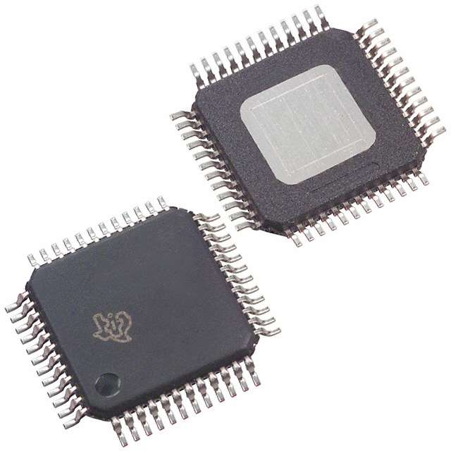
PACKAGE
PHP (48)
BODY SIZE (NOM)
7.00 mm × 7.00 mm
(1) For all available packages, see the orderable addendum at
the end of the data sheet.
Simplified Application
VBAT
BOOST
BUCK
VIN
XTALI
CPPx
TPS92662A
XTALO
MCU
BIN
ADCx
UART
RX
CAN
CAN
TX
ECU
I2C
E
2
LEDx
SDA
SCL
VDD
GND
1
An IMPORTANT NOTICE at the end of this data sheet addresses availability, warranty, changes, use in safety-critical applications,
intellectual property matters and other important disclaimers. PRODUCTION DATA.
�TPS92662A-Q1
SLUSDV6A – OCTOBER 2019 – REVISED JANUARY 2020
www.ti.com
Table of Contents
1
2
3
4
5
6
Features ..................................................................
Applications ...........................................................
Description .............................................................
Revision History.....................................................
Description (continued).........................................
Device and Documentation Support....................
1
1
1
2
2
3
6.1
6.2
6.3
6.4
6.5
7
Receiving Notification of Documentation Updates....
Support Resources ...................................................
Trademarks ...............................................................
Electrostatic Discharge Caution ................................
Glossary ....................................................................
3
3
3
3
3
Mechanical, Packaging, and Orderable
Information ............................................................. 3
4 Revision History
NOTE: Page numbers for previous revisions may differ from page numbers in the current version.
Changes from Original (October 2019) to Revision A
•
Page
Changed device status from Advance Information to Production Data ................................................................................. 1
5 Description (continued)
The internal charge pump rail supplies the gate drive voltage for the LED bypass switches. The low on-resistance
(RDS(on)) of the bypass switch minimizes conduction loss and power dissipation.
The TPS92662A-Q1 and TPS92662-Q1 both incorporate identical register settings for programming phase shift
and pulse width of each individual LED in the string and for reporting LED open and short circuit faults.
2
Submit Documentation Feedback
Copyright © 2019–2020, Texas Instruments Incorporated
Product Folder Links: TPS92662A-Q1
�TPS92662A-Q1
www.ti.com
SLUSDV6A – OCTOBER 2019 – REVISED JANUARY 2020
6 Device and Documentation Support
6.1 Receiving Notification of Documentation Updates
To receive notification of documentation updates, navigate to the device product folder on ti.com. In the upper
right corner, click on Alert me to register and receive a weekly digest of any product information that has
changed. For change details, review the revision history included in any revised document.
6.2 Support Resources
TI E2E™ support forums are an engineer's go-to source for fast, verified answers and design help — straight
from the experts. Search existing answers or ask your own question to get the quick design help you need.
Linked content is provided "AS IS" by the respective contributors. They do not constitute TI specifications and do
not necessarily reflect TI's views; see TI's Terms of Use.
6.3 Trademarks
E2E is a trademark of Texas Instruments.
All other trademarks are the property of their respective owners.
6.4 Electrostatic Discharge Caution
This integrated circuit can be damaged by ESD. Texas Instruments recommends that all integrated circuits be handled with
appropriate precautions. Failure to observe proper handling and installation procedures can cause damage.
ESD damage can range from subtle performance degradation to complete device failure. Precision integrated circuits may be more
susceptible to damage because very small parametric changes could cause the device not to meet its published specifications.
6.5 Glossary
SLYZ022 — TI Glossary.
This glossary lists and explains terms, acronyms, and definitions.
7 Mechanical, Packaging, and Orderable Information
The following pages include mechanical, packaging, and orderable information. This information is the most
current data available for the designated devices. This data is subject to change without notice and revision of
this document. For browser-based versions of this data sheet, refer to the left-hand navigation.
Submit Documentation Feedback
Copyright © 2019–2020, Texas Instruments Incorporated
Product Folder Links: TPS92662A-Q1
3
�IMPORTANT NOTICE AND DISCLAIMER
TI PROVIDES TECHNICAL AND RELIABILITY DATA (INCLUDING DATASHEETS), DESIGN RESOURCES (INCLUDING REFERENCE
DESIGNS), APPLICATION OR OTHER DESIGN ADVICE, WEB TOOLS, SAFETY INFORMATION, AND OTHER RESOURCES “AS IS”
AND WITH ALL FAULTS, AND DISCLAIMS ALL WARRANTIES, EXPRESS AND IMPLIED, INCLUDING WITHOUT LIMITATION ANY
IMPLIED WARRANTIES OF MERCHANTABILITY, FITNESS FOR A PARTICULAR PURPOSE OR NON-INFRINGEMENT OF THIRD
PARTY INTELLECTUAL PROPERTY RIGHTS.
These resources are intended for skilled developers designing with TI products. You are solely responsible for (1) selecting the appropriate
TI products for your application, (2) designing, validating and testing your application, and (3) ensuring your application meets applicable
standards, and any other safety, security, or other requirements. These resources are subject to change without notice. TI grants you
permission to use these resources only for development of an application that uses the TI products described in the resource. Other
reproduction and display of these resources is prohibited. No license is granted to any other TI intellectual property right or to any third
party intellectual property right. TI disclaims responsibility for, and you will fully indemnify TI and its representatives against, any claims,
damages, costs, losses, and liabilities arising out of your use of these resources.
TI’s products are provided subject to TI’s Terms of Sale (www.ti.com/legal/termsofsale.html) or other applicable terms available either on
ti.com or provided in conjunction with such TI products. TI’s provision of these resources does not expand or otherwise alter TI’s applicable
warranties or warranty disclaimers for TI products.
Mailing Address: Texas Instruments, Post Office Box 655303, Dallas, Texas 75265
Copyright © 2020, Texas Instruments Incorporated
�


 工商网监
湘ICP备2023018690号
工商网监
湘ICP备2023018690号

