Order
Now
Product
Folder
Support &
Community
Tools &
Software
Technical
Documents
TUSB211, TUSB211I
SLLSEO0D – MAY 2015 – REVISED OCTOBER 2017
TUSB211 USB 2.0 High Speed Signal Conditioner
1 Features
3 Description
•
•
•
The TUSB211 is a USB High-Speed (HS) signal
conditioner, designed to compensate for ISI signal
loss in a transmission channel.
1
•
•
•
•
Compatible with USB 2.0, OTG 2.0 and BC 1.2
Support for LS, FS, HS signaling
Active Power Consumption of 55 mW (Typical)
with 3.3-V Single Supply
Selectable Signal Gain Via External Pulldown
Resistor
Does Not Break DP, DM Trace
Scalable Solution – Daisy Chain Device for High
Loss Applications
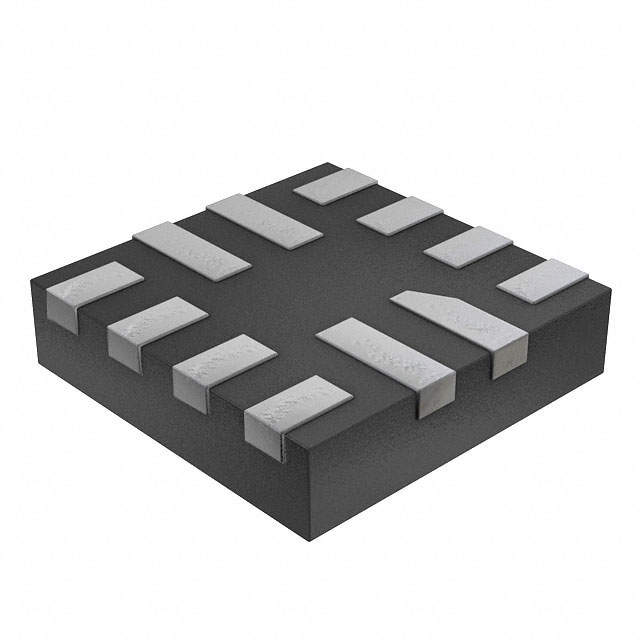
Compact 1.6 mm x 1.6 mm QFN Package
2 Applications
•
•
•
•
•
•
•
•
The device has a patent-pending design which is
agnostic to USB Low Speed (LS) and Full Speed
(FS) signals. LS and FS signal characteristics are
unaffected by the TUSB211. HS signals are
compensated.
Programmable signal gain permits fine tuning device
performance to optimize High Speed signals at the
connector. This helps to pass USB High Speed
electrical compliance tests.
The footprint of TUSB211 does not break the
continuity of the DP/DM signal path. This permits risk
free system design of a complete USB channel.
Notebooks
Desktops
Docking Stations
Cell Phones
Active Cable, Cable Extenders
Backplane
Televisions
Tablets
In addition, TUSB211 is compatible with the USB OnThe-Go (OTG) and Battery Charging (BC) protocols
Device Information
PART NUMBER
TUSB211
TUSB211I
PACKAGE
X2QFN (12)
(1)
BODY SIZE (NOM)
1.60 mm x 1.60 mm
(1) For all available packages, see the orderable addendum at
the end of the datasheet.
Simplified Schematic
USB Host Implementation
Programmable Logic
Device
[Optional]
USB Transceiver
5V
CD
D2P
TEST
ENA_HS RSTN
TUSB211
D2M
HS
RX
VCC
GND
EQ
D1P
DP
D1M
DM
VREG
USB Connector
VBUS
HS
TX
GND
3.3V
Host
Controller
TUSB211
Copyright © 2016, Texas Instruments Incorporated
1
An IMPORTANT NOTICE at the end of this data sheet addresses availability, warranty, changes, use in safety-critical applications,
intellectual property matters and other important disclaimers. PRODUCTION DATA.
�TUSB211, TUSB211I
SLLSEO0D – MAY 2015 – REVISED OCTOBER 2017
www.ti.com
Table of Contents
1
2
3
4
5
6
7
Features ..................................................................
Applications ...........................................................
Description .............................................................
Revision History.....................................................
Pin Configuration and Functions .........................
Specifications.........................................................
1
1
1
2
3
4
6.1
6.2
6.3
6.4
6.5
6.6
4
4
4
4
5
6
Absolute Maximum Ratings ......................................
ESD Ratings..............................................................
Recommended Operating Conditions.......................
Thermal Information ..................................................
Electrical Characteristics...........................................
Switching Characteristics ..........................................
Detailed Description .............................................. 7
7.1 Overview ................................................................... 7
7.2 Functional Block Diagram ......................................... 7
7.3 Device Functional Modes.......................................... 7
8
Application and Implementation .......................... 8
8.1 Application Information.............................................. 8
8.2 Typical Application ................................................... 8
9 Power Supply Recommendations...................... 11
10 Layout................................................................... 12
10.1 Layout Guidelines ................................................. 12
10.2 Layout Example .................................................... 12
11 Device and Documentation Support ................. 13
11.1
11.2
11.3
11.4
11.5
Related Links ........................................................
Community Resources..........................................
Trademarks ...........................................................
Electrostatic Discharge Caution ............................
Glossary ................................................................
13
13
13
13
13
12 Mechanical, Packaging, and Orderable
Information ........................................................... 13
4 Revision History
Changes from Revision C (June 2016) to Revision D
Page
•
Deleted device TUSB211-Q1 From the data sheet................................................................................................................ 1
•
Deleted Features: Qualified for Automotive Applications ....................................................................................................... 1
•
Deleted Applications: Automotive Infotainment ...................................................................................................................... 1
Changes from Revision A (June 2015) to Revision B
Page
•
Changed From: 1-page datasheet To: Full datasheet .......................................................................................................... 1
•
Added Features: Qualified for Automotive Applications ......................................................................................................... 1
•
Deleted Features: –40°C to 85°C Industrial Temperature Range.......................................................................................... 1
•
Added Applications: Automotive Infotainment ........................................................................................................................ 1
•
Changed the Simplified Schematic......................................................................................................................................... 1
Changes from Original (May 2015) to Revision A
•
2
Page
Changed the data sheet From: Product Preview To: Production .......................................................................................... 1
Submit Documentation Feedback
Copyright © 2015–2017, Texas Instruments Incorporated
Product Folder Links: TUSB211
�TUSB211, TUSB211I
www.ti.com
SLLSEO0D – MAY 2015 – REVISED OCTOBER 2017
5 Pin Configuration and Functions
RWB Package
12 Pin (X2QFN)
Top View
D1P D1M
12
VCC
TEST
3
CD
4
11 VREG
RSTN
5
10 GND
EQ
6
2
7
1
8
9
ENA_HS
D2P D2M
Pin Functions
PIN
NAME
VCC
NO.
12
INTERNAL
PULLUP/PULLDOWN
I/O
P
N/A
DESCRIPTION
3.3-V power
RSTN asserted: 30 kΩ PD
FS, LS mode: 30 kΩ PD
1.8-V LDO output. Only enabled when operating in High Speed mode.
Requires 0.1-µF external capacitor to GND to stabilize the core.
VREG
11
O
GND
10
P
N/A
Ground
RSTN
5
I
500 kΩ PU
Device disable/enable.
Recommend 0.1-µF external capacitor to GND to ensure clean power on
reset if not driven.
EQ
6
I
N/A
USB High Speed boost select via external pull down resistor.
Sampled upon power up.
Auto selects min EQ when left floating.
Does not recognize real time adjustments.
D1P
2
I/O
N/A
USB High Speed positive port.
Orientation independent – Can face either upstream or downstream.
D1M
1
I/O
N/A
USB High Speed negative port.
Orientation independent – Can face either upstream or downstream.
D2P
7
I/O
N/A
USB High Speed positive port.
Orientation independent – Can face either upstream or downstream.
D2M
8
I/O
N/A
USB High Speed negative port.
Orientation independent – Can face either upstream or downstream.
TEST
3
I
RSTN asserted: 500 kΩ PD
No function. Leave floating.
HS mode: N/A
Flag indicating that channel is in High Speed mode. Asserted upon:
ENA_HS
9
O
RSTN asserted: 500kΩ PD
1.
Detection of USB-IF High Speed test fixture from an unconnected
state followed by transmission of USB TEST_PACKET pattern.
2.
Squelch detection following USB reset with a successful HS
handshake [HS handshake is declared to be successful after single
chirp J chirp K pair where each chirp is within 18 µs – 128 µs]
De-asserted upon detection of disconnect or suspend.
Can be left floating if not needed.
CD
4
O
RSTN asserted: 500 kΩ PD
Flag indicating that a USB device is attached.
Asserted from an unconnected state upon detection of DP or DM pull-up
resistor.
De-asserted upon detection of disconnect.
Can be left floating if not needed.
Submit Documentation Feedback
Copyright © 2015–2017, Texas Instruments Incorporated
Product Folder Links: TUSB211
3
�TUSB211, TUSB211I
SLLSEO0D – MAY 2015 – REVISED OCTOBER 2017
www.ti.com
6 Specifications
6.1 Absolute Maximum Ratings
over operating free-air temperature range (unless otherwise noted)
(1)
MIN
MAX
UNIT
Supply voltage range
VCC
–0.3
3.8
V
Voltage range
D1P, D1M, D2P, D2M, RSTN, EQ
–0.3
3.8
V
–65
150
°C
Storage temperature, Tstg
(1)
Stresses beyond those listed under Absolute Maximum Ratings may cause permanent damage to the device. These are stress ratings
only, which do not imply functional operation of the device at these or any other conditions beyond those indicated under Recommended
Operating Conditions. Exposure to absolute-maximum-rated conditions for extended periods may affect device reliability.
6.2 ESD Ratings
VALUE
Human-body model (HBM), per ANSI/ESDA/JEDEC JS-001
V(ESD)
Electrostatic discharge
(1)
Charged-device model (CDM), per JEDEC specification JESD22-C101
±1000
(2)
(1)
(2)
UNIT
±3000
V
JEDEC document JEP155 states that 500-V HBM allows safe manufacturing with a standard ESD control process.
JEDEC document JEP157 states that 250-V CDM allows safe manufacturing with a standard ESD control process.
6.3 Recommended Operating Conditions
over operating free-air temperature range (unless otherwise noted)
VCC
TA
MIN
NOM
MAX
Supply voltage
3
3.3
3.6
Operating free-air temperature [TUSB211]
0
70
Operating free-air temperature [TUSB211I]
–40
85
UNIT
V
°C
6.4 Thermal Information
THERMAL METRIC
(1)
RWB
12 PINS
UNIT
RθJA
Junction-to-ambient thermal resistance
161.6
°C/W
RθJC(top)
Junction-to-case (top) thermal resistance
63.3
°C/W
RθJB
Junction-to-board thermal resistance
75.1
°C/W
ψJT
Junction-to-top characterization parameter
1.9
°C/W
ψJB
Junction-to-board characterization parameter
75.1
°C/W
RθJC(bot)
Junction-to-case (bottom) thermal resistance
N/A
°C/W
(1)
4
For more information about traditional and new thermal metrics, see the Semiconductor and IC Package Thermal Metrics application
report, SPRA953.
Submit Documentation Feedback
Copyright © 2015–2017, Texas Instruments Incorporated
Product Folder Links: TUSB211
�TUSB211, TUSB211I
www.ti.com
SLLSEO0D – MAY 2015 – REVISED OCTOBER 2017
6.5 Electrical Characteristics
over operating free-air temperature range (unless otherwise noted)
PARAMETER
TEST CONDITIONS
MIN
TYP
(1)
MAX
16
20
mA
UNIT
I(ACTIVE_HS)
High Speed Active Current
USB channel = HS mode. 480 Mbps
traffic. VCC supply stable
I(IDLE_HS)
High Speed Idle Current
USB channel = HS mode. No traffic. VCC
supply stable
12
15
mA
I(SUSPEND_HS) Suspend Current
USB channel = Suspend mode.
4.5
5.5
mA
I(FS)
Full-Speed Current
USB channel = FS mode
4.5
5.5
mA
I(LS)
Low-Speed Current
USB channel = LS mode
4.5
5.5
mA
I(DISCONN)
Disconnect Power
Host side application. No device
attachment.
4.5
5.5
mA
I(RSTN)
Disable Power
RSTN driven low; VCC supply stable; VCC
= 3.3 V
4.5
5.5
mA
RSTN
VIH
High level input voltage
2
VCC
V
VIL
Low-level input voltage
0
0.8
V
IIH
High level input current
VIH = 3.6 V, VCC = 3 V, RPU enabled
±2
µA
IIL
Low level input current
VIL = 0V, VCC = 3.6 V, RPU enabled
±11
µA
EQ
Level 0 EQ
R(EQ)
External pulldown resistor
0.32
kΩ
Level 1 EQ
1.4
2.2
kΩ
Level 2 EQ [MAX]
3.7
4.1
kΩ
Level 3 EQ [MIN]
6
kΩ
CD, ENA_HS
VOH
High level output voltage
IO = –50 µA
VOL
Low level output voltage
IO = 50 µA
T(SHRT_GND)
DP, DM low voltage short circuit
DxP or DxM short circuited to GND
continuously for 24 hours
at TA = 25°C only
CIO(DXX)
Capacitance to GND
Measured with LCR meter and device
powered down. 1 MHz sinusoid, 30 mVpp
ripple
2.4
V
0.4
V
DxP, DxM
(1)
0
V
5
pF
(1) All typical values are at VCC = 3.3 V, and TA = 25°C.
Submit Documentation Feedback
Copyright © 2015–2017, Texas Instruments Incorporated
Product Folder Links: TUSB211
5
�TUSB211, TUSB211I
SLLSEO0D – MAY 2015 – REVISED OCTOBER 2017
www.ti.com
6.6 Switching Characteristics
over operating free-air temperature range (unless otherwise noted)
PARAMETER
TEST CONDITIONS
MIN
TYP
(1)
MAX
UNIT
480
Mbps
DxP, DxM
F(BR_DXX)
Bit Rate
t(R/F_DXX)
Rise/Fall time
USB channel = HS mode. 480 Mbps
traffic. VCC supply stable
100
ps
CD, ENA_HS
t(EN)
Enable time
20
µs
t(DIS)
Disable time
20
µs
VCC
t(STABLE)
VCC stable before RSTN de-assertion
100
t(RAMP)
VCC ramp time
0.2
(1)
6
µs
100
ms
(1) All typical values are at VCC = 3.3 V, and TA = 25°C.
Submit Documentation Feedback
Copyright © 2015–2017, Texas Instruments Incorporated
Product Folder Links: TUSB211
�TUSB211, TUSB211I
www.ti.com
SLLSEO0D – MAY 2015 – REVISED OCTOBER 2017
7 Detailed Description
7.1 Overview
The TUSB211 is a USB High-Speed (HS) signal conditioner, designed to compensate for ISI signal loss in a
transmission channel. TUSB211 has a patent-pending design which is agnostic to USB Low Speed (LS) and Full
Speed (FS) signals and does not alter their signal characteristics, while HS signals are compensated. In addition,
the design is compatible with USB On-The-Go (OTG) and Battery Charging (BC) specifications.
Programmable signal gain through an external resistor permits fine tuning device performance to optimize signals
helping to pass USB HS electrical compliance tests at the connector.
The footprint of TUSB211 allows a board layout using this device such that it does not break the continuity of the
DP/DM signal traces. This permits risk free system design of a complete USB channel with flexible use of one or
multiple TUSB211 devices as needed for optimal signal integrity. This allows system designers to plan for this
device and use it only if signal integrity analysis and/or lab measurements show a need. If such a need is not
warranted, the device can be left unpopulated without any board rework.
7.2 Functional Block Diagram
TUSB211
Low and Full
Speed Bypass
USB
TRANSCEIVER
OPTIONAL
PLD
D2P
D2M
CD
ENA_HS
High Speed
Compensation
D1P
D1M
ESD
PROTECTION
USB
CONNECTOR
Status flags
Copyright © 2016, Texas Instruments Incorporated
7.3 Device Functional Modes
7.3.1 Low Speed (LS) Mode
TUSB211 automatically detects a LS connection and does not enable signal compensation. CD pin is asserted
high.
7.3.2 Full Speed (FS) Mode
TUSB211 automatically detects a FS connection and does not enable signal compensation. CD pin is asserted
high.
7.3.3 High Speed (HS) Mode
TUSB211 automatically detects a HS connection and enables signal compensation as determined by the
configuration of the external pulldown resistance on its EQ pin. ENA_HS pin asserted high in addition to the CD
pin.
7.3.4 Disable Mode
TUSB211 can be disabled when its RSTN pin is asserted low. The USB channel is still fully operational, but there
is neither signal compensation, nor any indication from the CD pin or ENA_HS pin as to the status of the
channel.
Submit Documentation Feedback
Copyright © 2015–2017, Texas Instruments Incorporated
Product Folder Links: TUSB211
7
�TUSB211, TUSB211I
SLLSEO0D – MAY 2015 – REVISED OCTOBER 2017
www.ti.com
8 Application and Implementation
NOTE
Information in the following applications sections is not part of the TI component
specification, and TI does not warrant its accuracy or completeness. TI’s customers are
responsible for determining suitability of components for their purposes. Customers should
validate and test their design implementation to confirm system functionality.
8.1 Application Information
The primary purpose of the TUSB211 is to re-store the signal integrity of a USB High Speed channel up to the
USB connector. The loss in signal quality stems from reduced channel bandwidth due to high loss PCB trace and
other components that contribute a capacitive load. This can cause the channel to fail the USB near end eye
mask. Proper use of the TUSB211 can help to pass this eye mask.
A secondary purpose is to use the CD pin and ENA_HS pin of the TUSB211 to control other blocks on the
customer platform if so desired.
8.2 Typical Application
A typical application is shown below. In this setup, D1P and D1M face the USB connector while D2P and D2M
face the USB transceiver. If desired, the orientation may be reversed [that is, D1 faces transceiver and D2 faces
connector].
Note that CD and ENA_HS are connected to PLDs. This is for platforms where other circuit blocks must be
modified based on the status of the USB channel. They could also be connected to LEDs to give a physical
indication of current channel status for debug purposes. If neither use is desired, they can be left floating.
Copyright © 2016, Texas Instruments Incorporated
Figure 1. Reference Schematic
8
Submit Documentation Feedback
Copyright © 2015–2017, Texas Instruments Incorporated
Product Folder Links: TUSB211
�TUSB211, TUSB211I
www.ti.com
SLLSEO0D – MAY 2015 – REVISED OCTOBER 2017
Typical Application (continued)
8.2.1 Design Requirements
TUSB211 requires a valid reset signal as described in the power supply recommendations section. The capacitor
C4 is not required if a microcontroller drives the RSTN pin according to recommendations.
Pin 11 VREG is an internal LDO output that requires a 0.1 μF external capacitor to GND to stabilize the core.
Pin 6 EQ requires an external pulldown resistor if EQ levels 0-2 are needed. If EQ level 3 is needed, then the EQ
pin can be left floating.
8.2.2 Detailed Design Procedure
The ideal EQ setting is dependent upon the signal chain loss characteristics of the target platform. The general
recommendation is to start with EQ level 0, and then increment to EQ level 1, and so on. if permissible.
In order for the TUSB211 to recognize any change to the EQ setting, the RSTN pin must be toggled. This is
because the EQ pin is latched on power up and the pin is ignored thereafter.
In addition, TUSB211 does not compensate for any DC attenuation in the signal path. Therefore, minimizing DC
loss (that is, resistance) in the system design, is suggested. As a consequence, this might lead to increased line
capacitance. This is acceptable because the TUSB211 can compensate for the additional capacitive load.
Placement of the device is also dependent on the application goal. Table 1 summarizes the recommendations.
Table 1. TUSB211 Platform Placement Guideline
PLATFORM GOAL
SUGGESTED TUSB211 PLACEMENT
Pass USB Near End Mask
Close to measurement point
Pass USB Far End Eye Mask
Close to USB PHY
Cascade multiple 211s to improve device enumeration
Midway between each USB interconnect
NOTE
USB-IF certification tests for High Speed eye masks require the mandated use of the
USB-IF developed test fixtures. These test fixtures do not require the use of oscilloscope
probes. Instead they use SMA cables. More information can be found at the USB-IF
Compliance Updates Page. It is located under the ‘Electricals’ section, ID 86 dated March
2013.
The following procedure must be followed before using any oscilloscope compliance software to construct a USB
High Speed Eye Mask:
8.2.2.1 For a Host Side Application
1.
2.
3.
4.
5.
6.
Configure the TUSB211 to the desired EQ setting
Power on (or toggle the RSTN pin if already powered on) the TUSB211
Using SMA cables, connect the oscilloscope and the USB-IF host-side test fixture to the TUSB211
Enable the host to transmit USB TEST_PACKET
Execute the oscilloscope’s USB compliance software.
Repeat the above steps in order to re-test TUSB211 with a different EQ setting
Submit Documentation Feedback
Copyright © 2015–2017, Texas Instruments Incorporated
Product Folder Links: TUSB211
9
�TUSB211, TUSB211I
SLLSEO0D – MAY 2015 – REVISED OCTOBER 2017
www.ti.com
8.2.2.2 For a Device Side Application
1. Configure the TUSB211 to the desired EQ setting
2. Power on (or toggle the RSTN pin if already powered on) the TUSB211
3. Connect a USB host, the USB-IF device-side test fixture, and USB device to the TUSB211. Ensure that the
USB-IF device test fixture is configured to the ‘INIT’ position
4. Allow the host to enumerate the device
5. Enable the device to transmit USB TEST_PACKET
6. Using SMA cables, connect the oscilloscope to the USB-IF device-side test fixture and ensure that the
device-side test fixture is configured to the ‘TEST’ position.
7. Execute the oscilloscope’s USB compliance software.
8. Repeat the above steps in order to re-test TUSB211 with a different EQ setting
8.2.3 Application Curves
2m USB 3.0 cable
USB-IF SMA Fixture
TUSB211
EVM
USB Host
A
TEST_PACKET
transmission
B
Agilent
16 GHz
Scope
A
Figure 2. Eye Diagram Bench Setup
0.4
Differential Signal (V)
Differential Signal (V)
0.4
0.2
0.0
-0.2
-0.4
0.2
0.0
-0.2
-0.4
0
0.5
1
Time (ns)
1.5
2
0
Figure 3. TUSB211 Disabled
10
0.5
1
Time (ns)
1.5
2
Figure 4. EQ Level 0
Submit Documentation Feedback
Copyright © 2015–2017, Texas Instruments Incorporated
Product Folder Links: TUSB211
�TUSB211, TUSB211I
www.ti.com
SLLSEO0D – MAY 2015 – REVISED OCTOBER 2017
0.4
Differential Signal (V)
Differential Signal (V)
0.4
0.2
0.0
-0.2
-0.4
0.2
0.0
-0.2
-0.4
0
0.5
1
Time (ns)
1.5
2
0
0.5
Figure 5. EQ Level 1
1
Time (ns)
1.5
2
Figure 6. EQ Level 2
Differential Signal (V)
0.4
0.2
0.0
-0.2
-0.4
0
0.5
1
Time (ns)
1.5
2
Figure 7. EQ Level 3
9 Power Supply Recommendations
On power up, the interaction of the RSTN pin and power on ramp could result in digital circuits not being set
correctly. The device should not be enabled until the power on ramp has settled to 3 V or higher to guarantee a
correct power on reset of the digital circuitry. If RSTN cannot be held low by microcontroller or other circuitry until
the power on ramp has settled, then an external capacitor from the RSTN pin to GND is required to hold the
device in the low power reset state.
The RC time constant should be larger than five times of the power on ramp time (0 to VCC). With a typical
internal pullup resistance of 500 kΩ, the recommended minimum external capacitance is calculated as:
[Ramp Time x 5] ÷ [500 kΩ]
(1)
Submit Documentation Feedback
Copyright © 2015–2017, Texas Instruments Incorporated
Product Folder Links: TUSB211
11
�TUSB211, TUSB211I
SLLSEO0D – MAY 2015 – REVISED OCTOBER 2017
www.ti.com
10 Layout
10.1 Layout Guidelines
There is no need to break the USB signal trace. Thus, even with the TUSB211 powered down, or not populated,
the USB link is still fully operational. To avoid the need for signal vias, routing the High Speed traces directly
underneath the TUSB211 package, as illustrated in the PCB land pattern shown in Figure 8, is recommended.
Although the land pattern shown below has matched trace width to pad width, optimal impedance control is
based on the user's own PCB stack-up. It is recommended to maintain 90 Ω differential routing underneath the
device.
All dimensions are in millimetres (mm).
10.2 Layout Example
Figure 8. DP and DM Routing Underneath Device Package
12
Submit Documentation Feedback
Copyright © 2015–2017, Texas Instruments Incorporated
Product Folder Links: TUSB211
�TUSB211, TUSB211I
www.ti.com
SLLSEO0D – MAY 2015 – REVISED OCTOBER 2017
11 Device and Documentation Support
11.1 Related Links
The table below lists quick access links. Categories include technical documents, support and community
resources, tools and software, and quick access to order now.
Table 2. Related Links
PARTS
PRODUCT FOLDER
ORDER NOW
TECHNICAL
DOCUMENTS
TOOLS &
SOFTWARE
SUPPORT &
COMMUNITY
TUSB211
Click here
Click here
Click here
Click here
Click here
TUSB211I
Click here
Click here
Click here
Click here
Click here
11.2 Community Resources
The following links connect to TI community resources. Linked contents are provided "AS IS" by the respective
contributors. They do not constitute TI specifications and do not necessarily reflect TI's views; see TI's Terms of
Use.
TI E2E™ Online Community TI's Engineer-to-Engineer (E2E) Community. Created to foster collaboration
among engineers. At e2e.ti.com, you can ask questions, share knowledge, explore ideas and help
solve problems with fellow engineers.
Design Support TI's Design Support Quickly find helpful E2E forums along with design support tools and
contact information for technical support.
11.3 Trademarks
E2E is a trademark of Texas Instruments.
All other trademarks are the property of their respective owners.
11.4 Electrostatic Discharge Caution
These devices have limited built-in ESD protection. The leads should be shorted together or the device placed in conductive foam
during storage or handling to prevent electrostatic damage to the MOS gates.
11.5 Glossary
SLYZ022 — TI Glossary.
This glossary lists and explains terms, acronyms, and definitions.
12 Mechanical, Packaging, and Orderable Information
The following pages include mechanical, packaging, and orderable information. This information is the most
current data available for the designated devices. This data is subject to change without notice and revision of
this document. For browser-based versions of this data sheet, refer to the left-hand navigation.
Submit Documentation Feedback
Copyright © 2015–2017, Texas Instruments Incorporated
Product Folder Links: TUSB211
13
�PACKAGE OPTION ADDENDUM
www.ti.com
10-Dec-2020
PACKAGING INFORMATION
Orderable Device
Status
(1)
Package Type Package Pins Package
Drawing
Qty
Eco Plan
(2)
Lead finish/
Ball material
MSL Peak Temp
Op Temp (°C)
Device Marking
(3)
(4/5)
(6)
TUSB211IRWBR
ACTIVE
X2QFN
RWB
12
3000
RoHS & Green
NIPDAU
Level-2-260C-1 YEAR
-40 to 85
I1
TUSB211RWBR
ACTIVE
X2QFN
RWB
12
3000
RoHS & Green
NIPDAU
Level-2-260C-1 YEAR
0 to 70
C1
(1)
The marketing status values are defined as follows:
ACTIVE: Product device recommended for new designs.
LIFEBUY: TI has announced that the device will be discontinued, and a lifetime-buy period is in effect.
NRND: Not recommended for new designs. Device is in production to support existing customers, but TI does not recommend using this part in a new design.
PREVIEW: Device has been announced but is not in production. Samples may or may not be available.
OBSOLETE: TI has discontinued the production of the device.
(2)
RoHS: TI defines "RoHS" to mean semiconductor products that are compliant with the current EU RoHS requirements for all 10 RoHS substances, including the requirement that RoHS substance
do not exceed 0.1% by weight in homogeneous materials. Where designed to be soldered at high temperatures, "RoHS" products are suitable for use in specified lead-free processes. TI may
reference these types of products as "Pb-Free".
RoHS Exempt: TI defines "RoHS Exempt" to mean products that contain lead but are compliant with EU RoHS pursuant to a specific EU RoHS exemption.
Green: TI defines "Green" to mean the content of Chlorine (Cl) and Bromine (Br) based flame retardants meet JS709B low halogen requirements of


 工商网监
湘ICP备2023018690号
工商网监
湘ICP备2023018690号
