Product
Folder
Order
Now
Support &
Community
Tools &
Software
Technical
Documents
TUSB215
SLLSEX8B – AUGUST 2017 – REVISED SEPTEMBER 2017
TUSB215 USB 2.0 High Speed Signal Conditioner with USB BC1.2 CDP
1 Features
3 Description
•
•
•
The TUSB215 is a USB High-Speed (HS) signal
conditioner, designed to compensate for ISI signal
loss in a transmission channel which helps passing
USB electrical compliance tests.
1
•
•
•
•
•
Compatible with USB 2.0, OTG 2.0 and BC 1.2
Pin strap or I2C Configurable
USB BC1.2 Charging Downstream Port (CDP)
controller
Support for LS, FS, HS signaling
Ultra-low USB Disconnect and Shutdown Power
Consumption
Scalable solution - Daisy Chain Device for High
Loss Applications
D1P/M and D2P/M Interchangeable and
Host/Device Agnostic
Supports up to 5m pre-channel or 2m postchannel Cable Length
– Four Selectable AC Boost Setting Via External
Pulldown Resistor
– DC Boost Along With AC Boost for Best Signal
Integrity
TUSB215 has a patent-pending design which is
agnostic to USB Low Speed (LS) and Full Speed
(FS) signals. LS and FS signal characteristics are
unaffected by the TUSB215 while HS signals are
compensated.
Programmable signal AC boost and DC boost permits
fine tuning device performance to optimize High
Speed signals at the connector, this allows use in
many different applications.
In addition, TUSB215 is compatible with the USB OnThe-Go (OTG) and Battery Charging (BC) protocols.
TUSB215 further acts as Charging Downstream Port
(CDP) controller and handles the necessary
handshakes with the downstream device.
Device Information
2 Applications
•
•
•
•
•
•
•
•
PART NUMBER
TUSB215
Notebooks
Desktops
Docking Stations
Tablets
Cell Phones
Active Cable, Cable Extenders
Backplane
Televisions
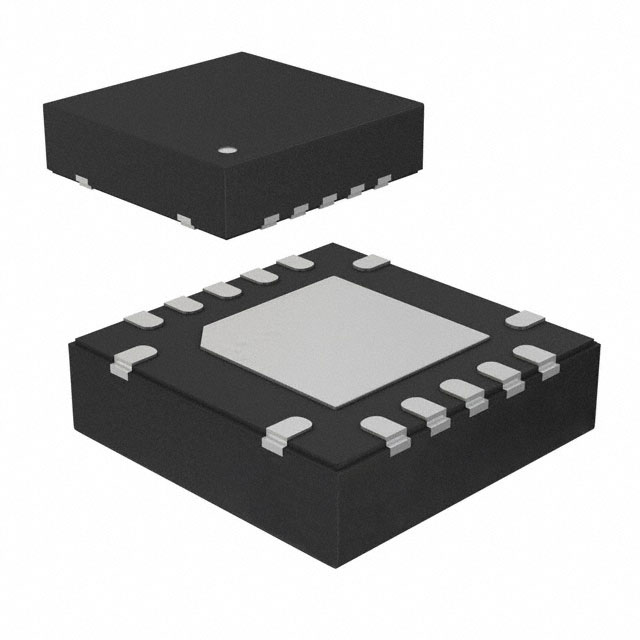
PACKAGE
VQFN (14)
TUSB215I
(1)
BODY SIZE (NOM)
3.50 mm x 3.50 mm
(1) For all available packages, see the orderable addendum at
the end of the datasheet.
SPACER
SPACER
Simplified Schematic
5V
VCC
USB Host
DP
DM
Cable
D1P
D2P
D1M
D2M
DP
USB
DM Connector
GND
Copyright © 2017, Texas Instruments Incorporated
1
An IMPORTANT NOTICE at the end of this data sheet addresses availability, warranty, changes, use in safety-critical applications,
intellectual property matters and other important disclaimers. PRODUCTION DATA.
�TUSB215
SLLSEX8B – AUGUST 2017 – REVISED SEPTEMBER 2017
www.ti.com
Table of Contents
1
2
3
4
5
6
7
Features ..................................................................
Applications ...........................................................
Description .............................................................
Revision History.....................................................
Pin Configuration and Functions .........................
Specifications.........................................................
1
1
1
2
3
4
6.1
6.2
6.3
6.4
6.5
6.6
6.7
4
4
4
5
5
6
7
Absolute Maximum Ratings ......................................
ESD Ratings..............................................................
Recommended Operating Conditions.......................
Thermal Information ..................................................
Electrical Characteristics...........................................
Switching Characteristics ..........................................
Typical Characteristics ..............................................
Detailed Description .............................................. 8
7.1 Overview ................................................................... 8
7.2 Functional Block Diagram ......................................... 8
7.3 Feature Description................................................... 8
7.4 Device Functional Modes.......................................... 9
8
Application and Implementation ........................ 11
8.1 Application Information............................................ 11
8.2 Typical Application ................................................. 11
9 Power Supply Recommendations...................... 18
10 Layout................................................................... 19
10.1 Layout Guidelines ................................................. 19
10.2 Layout Example .................................................... 19
11 Device and Documentation Support ................. 20
11.1
11.2
11.3
11.4
11.5
Receiving Notification of Documentation Updates
Community Resources..........................................
Trademarks ...........................................................
Electrostatic Discharge Caution ............................
Glossary ................................................................
20
20
20
20
20
12 Mechanical, Packaging, and Orderable
Information ........................................................... 20
4 Revision History
Changes from Revision A (August 2017) to Revision B
Page
•
Changed Note From: Pull-up resistors for SDA and SCL pins in I2C mode should be 2 kΩ (5%). To: Pull-up resistors
for SDA and SCL pins in I2C mode should be 4.7 kΩ (5%) in the Pin Functions table.......................................................... 3
•
Added Test Conditions to RSTN: VIH and VIL in the Electrical Characteristics table.............................................................. 5
•
Added new parameters to SCL/SDA: VIH, VIL, VSDA_OL, ISDA_OL the Electrical Characteristics table ..................................... 5
•
Added Test Conditions To: DC_BOOST: VIH, VIM, and VIL the Electrical Characteristics table ............................................. 5
•
Added test conditions to trise_dxx and tfall_dxx in the Switching Characteristics table ................................................................. 6
Changes from Original (August 2017) to Revision A
•
2
Page
Changed CIO_DXX TYP value From: 7 pF To: 2.7 pF in the Electrical Characteristics table ................................................... 6
Submit Documentation Feedback
Copyright © 2017, Texas Instruments Incorporated
Product Folder Links: TUSB215
�TUSB215
www.ti.com
SLLSEX8B – AUGUST 2017 – REVISED SEPTEMBER 2017
5 Pin Configuration and Functions
NC
2
NC
3
14
1
EQ
RSTN
RGY Package
14 Pin (VQFN)
Top View
13
SCL/CD
12
VCC
11
SDA
Thermal
Pad
D2P
5
10
D1P
D2M
6
9
D1M
GND
VREG
8
4
7
DC_BOOST/ENA_HS
Not to scale
Pin Functions
PIN
NAME
NO.
INTERNAL
PULLUP/PULLDOWN
I/O
DESCRIPTION
EQ
1
I
N/A
USB High Speed AC boost select via external pull down resistor.
Sampled upon de-assertion of RSTN. Does not recognize real time
adjustments.
See application section for details. Auto selects maximum AC boost level
when left floating.
NC
2, 3
N/A
N/A
Leave unconnected.
In I2C mode:
Reserved for TI test purpose.
In non-I2C mode:
At reset: 3-level input signal DC_BOOST. USB High Speed DC signal boost
selection.
H (pin is pulled high) – 80 mV
M (pin is left floating) – 60 mV
L (pin is pulled low) – 40 mV
After reset: Output signal ENA_HS. Flag indicating that channel is in High
Speed mode. Asserted upon:
1. Detection of USB-IF High Speed test fixture from an unconnected state
followed by transmission of USB TEST_PACKET pattern.
2. Squelch detection following USB reset with a successful HS handshake [HS
handshake is declared to be successful after single chirp J chirp K pair where
each chirp is within 18 μs – 128 μs].
DC_BOOST (1
)
/ENA_HS
4
I/O
D2P
5
I/O
N/A
USB High Speed positive port.
D2M
6
I/O
N/A
USB High Speed negative port.
GND
7
PWR
N/A
Ground
VREG
8
O
N/A
1.8-V LDO output. Only enabled when operating in High Speed mode.
Requires 0.1-µF external capacitor to GND to stabilize the core.
D1M
9
I/O
N/A
USB High Speed negative port..
D1P
10
I/O
N/A
USB High Speed positive port.
SDA (2)
11
I/O
RSTN asserted: 500 kΩ PD
I2C Mode:
Bidirectional I2C data pin [I2C address = 0x2C].
In non I2C mode:
Reserved for TI test purpose.
(1)
(2)
Pull-down and pull-up (to 3.3 V) resistors for DC_BOOST pins must be between 22 kΩ to 47 kΩ in non I2C mode.
Pull-up resistors for SDA and SCL pins in I2C mode should be 4.7 kΩ (5%). If both SDA and SCL are pulled up at reset the device
enters into I2C mode.
Submit Documentation Feedback
Copyright © 2017, Texas Instruments Incorporated
Product Folder Links: TUSB215
3
�TUSB215
SLLSEX8B – AUGUST 2017 – REVISED SEPTEMBER 2017
www.ti.com
Pin Functions (continued)
PIN
NAME
VCC
12
SCL (2)/CD
PWR
13
RSTN
INTERNAL
PULLUP/PULLDOWN
I/O
NO.
14
I/O
I
DESCRIPTION
N/A
Supply power
RSTN asserted: 500 kΩ PD
In I2C mode:
I2C clock pin [I2C address = 0x2C].
Non I2C mode:
After reset: Output CD. Flag indicating that a USB device is attached
(connection detected). Asserted from an unconnected state upon detection of
DP or DM pull-up resistor. De-asserted upon detection of disconnect.
500 kΩ PU
Device disable/enable.
Low – Device is at reset and in shutdown, and
High – Normal operation.
Recommend 0.1-µF external capacitor to GND to ensure clean power on reset
if not driven.
If the pin is driven, it must be held low until the supply voltage for the device
reaches within specifications.
6 Specifications
6.1 Absolute Maximum Ratings
over operating free-air temperature and voltage range (unless otherwise noted) (1)
MIN
MAX
UNIT
VCC
-0.3
6
V
Voltage Range
on I/O pins
DxP, DxM, RSTN, EQ, SCL, SDA, DC_BOOST, VREG
-0.3
3.8
V
Tstg
Storage temperature
-65
150
°C
Supply Voltage
Range
(1)
Stresses beyond those listed under Absolute Maximum Rating may cause permanent damage to the device. These are stress ratings
only, which do not imply functional operation of the device at these or any other conditions beyond those indicated under Recommended
Operating Condition. Exposure to absolute-maximum-rated conditions for extended periods may affect device reliability.
6.2 ESD Ratings
VALUE
V(ESD)
(1)
(2)
Electrostatic discharge
Human body model (HBM), per
ANSI/ESDA/JEDEC JS-001, all pins (1)
±2000
Charged device model (CDM), per JEDEC
specification JESD22-C101, all pins (2)
±500
UNIT
V
JEDEC document JEP155 states that 500-V HBM allows safe manufacturing with a standard ESD control process.
JEDEC document JEP157 states that 250-V CDM allows safe manufacturing with a standard ESD control process.
6.3 Recommended Operating Conditions
over operating free-air temperature and voltage range (unless otherwise noted)
VCC
Supply voltage
TA
Ambient temperature
TJ
4
Junction temperature
MIN
NOM
MAX
4.4
5
5.5
UNIT
V
TUSB215
0
70
°C
TUSB215I
-40
85
°C
TUSB215
0
85
°C
TUSB215I
-40
105
°C
Submit Documentation Feedback
Copyright © 2017, Texas Instruments Incorporated
Product Folder Links: TUSB215
�TUSB215
www.ti.com
SLLSEX8B – AUGUST 2017 – REVISED SEPTEMBER 2017
6.4 Thermal Information
TUSB215
THERMAL METRIC (1)
RGY (VQFN)
UNIT
14 PINS
RθJA
Junction-to-ambient thermal resistance
49.1
°C/W
RθJC(top)
Junction-to-case (top) thermal resistance
52.8
°C/W
RθJB
Junction-to-board thermal resistance
24.2
°C/W
ΨJT
Junction-to-top characterization parameter
2.2
°C/W
ΨJB
Junction-to-board characterization parameter
24.3
°C/W
RθJC(bot)
Junction-to-case (bottom) thermal resistance
7
°C/W
(1)
For more information about traditional and new thermal metrics, see the Semiconductor and IC Package Thermal Metrics application
report.
6.5 Electrical Characteristics
over operating free-air temperature and voltage range (unless otherwise noted)
PARAMETER
TEST CONDITIONS
MIN
TYP
MAX
UNIT
POWER
High-speed active curent
USB channel = HS mode; 480 Mbps
traffic; VCC = 5V; VCC supply stable; DC
Boost = 60 mV
18
30
mA
IIDLE_HS
High-speed idle current
USB channel = HS mode; no traffic; VCC
= 5V; VCC supply stable; DC Boost = 60
mV
13
22
mA
ISUSPEND
High-speed suspend current
USB channel = HS suspend mode; VCC
= 5V; VCC supply stable
0.76
1.5
mA
IFS_LS
Full/Low speed current
USB channel = FS mode or LS mode;
VCC = 5V
0.77
1.5
mA
IDISCONN
Disconnect current
Host side application; No device
attachment; VCC = 5V
0.86
1.5
mA
IRSTN
Disable current
RSTN driven low; VCC supply stable; VCC
= 5V
22
80
µA
ILKG_FS
Pin fail-safe leakage current for SDA,
SCL, DC_BOOST, DxP/N, RSTN
VCC = 0 V; Pin at 3.6 V
40
µA
VIH
High-level input voltage
VCC = 4.4V
2
3.6
V
VIL
Low-level input voltage
VCC = 5.5V
0
0.8
V
IIH
High-level input current
VIH = 3.6 V
-4
4
µA
IIL
Low-level input current
VIL = 0 V
-11
11
µA
160
Ω
IACTIVE_H
S
_HS
ECT
RSTN
EQ
AC Boost Level 0
REQ
External pull-down resistor on EQ pin.
AC Boost Level 1
1.4
2
kΩ
AC Boost Level 2
3.7
3.9
kΩ
AC Boost Level 3
6
kΩ
CD, ENA_HS
VOH
High-level output voltage
IO = -50µA
VOL
Low-level output voltage
IO = 50µA
2.4
V
0.4
V
4
150
pF
2
3.6
V
0.8
V
SCL, SDA
CI2CBUS
I2C Bus capacitance
VIH
SDA and SCL input high level voltage
VCC = 4.4V
VIL
SDA and SCL input Low level voltage
VCC = 5.5V
VSDA_OL
SDA low-level output voltage
4.7kΩ pullup to 3.6V; VCC = 4.4V
ISDA_OL
SDA Low level output current
VCC = 5.5V; I2C pulled up to 3.6V
0.4
1.1
Submit Documentation Feedback
Copyright © 2017, Texas Instruments Incorporated
Product Folder Links: TUSB215
V
mA
5
�TUSB215
SLLSEX8B – AUGUST 2017 – REVISED SEPTEMBER 2017
www.ti.com
Electrical Characteristics (continued)
over operating free-air temperature and voltage range (unless otherwise noted)
PARAMETER
TEST CONDITIONS
MIN
TYP
MAX
UNIT
DC_BOOST
VIH
High-level input voltage
VCC = 5V
VIM
Mid-level input voltage
VCC = 5V
2.4
VIL
Low-level input voltage
VCC = 5V
Capacitance to GND
Measured with LCR meter and device
powered down. 1 MHz sinusoid, 30
mVpp ripple
3.6
1.6
0
V
V
0.4
V
DxP, DxM
CIO_DXX
2.7
pF
6.6 Switching Characteristics
over operating free-air temperature and voltage range (unless otherwise noted)
PARAMETER
FBR_DXX
TEST CONDITIONS
MIN
USB channel = HS mode; 480 Mbps
traffic; VCC supply stable
DxP/M Bit Rate
TYP
MAX
UNIT
480.24
Mbps
tRISE_DXX DxP/M rise time
10% - 90%; VCC = 5.5V; Max AC Gain;
100
ps
tFALL_DXX DxP/M fall time
90% - 10%; VCC = 5.5V; Max AC Gain;
100
ps
20
µs
100
µs
tRSTN_PU
LSE_WIDT
H
Minimum width to detect a valid RSTN
signal assert when the pin is actively
driven
VCC = 4.4 V; Refer to Figure 1
tSTABLE
VCC stable before RSTN de-assertion
Refer to Figure 1
tVCC_RAM
VCC ramp time
0.2
100
ms
P
tRSTN_PULSE_WIDTH
RSTN
VIL(MAX)
tSTABLE
VCC(MIN)
VCC
Figure 1. Power On and Reset Timing
6
Submit Documentation Feedback
Copyright © 2017, Texas Instruments Incorporated
Product Folder Links: TUSB215
�TUSB215
www.ti.com
SLLSEX8B – AUGUST 2017 – REVISED SEPTEMBER 2017
6.7 Typical Characteristics
Figure 2. USB2.0 HS Eye diagram, Host far-end with 2m
cable post-channel loss without TUSB215
Figure 3. USB2.0 HS Eye diagram, Host far-end with 2m
cable post-channel loss with TUSB215
Figure 4. USB2.0 HS Eye diagram, Host far-end with 5m
cable pre-channel loss without TUSB215
Figure 5. USB2.0 HS Eye diagram, Host far-end with 5m
cable pre-channel loss with TUSB215
Submit Documentation Feedback
Copyright © 2017, Texas Instruments Incorporated
Product Folder Links: TUSB215
7
�TUSB215
SLLSEX8B – AUGUST 2017 – REVISED SEPTEMBER 2017
www.ti.com
7 Detailed Description
7.1 Overview
The TUSB215 is a USB High-Speed (HS) signal conditioner, designed to compensate for ISI signal loss in a
transmission channel. TUSB215 has a patent-pending design which is agnostic to USB Low Speed (LS) and Full
Speed (FS) signals and does not alter their signal characteristics, while HS signals are compensated. In addition,
the design is compatible with USB On-The-Go (OTG) and Battery Charging (BC) specifications. The TUSB215
provides USB Charging Downstream Port (CDP) controller for applications in which USB host or hub do not have
this function.
Programmable signal AC boost through an external resistor on EQ pin permits fine tuning device performance to
optimize signals helping to pass USB HS electrical compliance tests at the connector. Additional DC Boost
configurable by three level input DC_BOOST pin helps overcoming the cable losses.
7.2 Functional Block Diagram
Low and Full
Speed Bypass
USB
TRANSCEIVER
OPTIONAL
PLD
D1P
D1M
D2P
High Speed
Compensation
ESD
PROTECTION
D2M
USB
CONNECTOR
CDP Controller
CD
Status Flags
ENA_HS
7.3 Feature Description
7.3.1 EQ
The EQ pin of the TUSB215 is used to configure the AC boost of the device. The four levels of AC boost are set
through different values of an external pulldown resistor at this pin.
7.3.2 DC BOOST
The DC_BOOST pin of the TUSB215 is a tri-level pin, used to set the DC gain of the device according to
Table 1.
Table 1. DC Boost Settings
DC BOOST SETTING VIA PIN STRAP
8
DC_BOOST
DC Boost Setting (mV)
VIL
40
VIM
60
VIH
80
Submit Documentation Feedback
Copyright © 2017, Texas Instruments Incorporated
Product Folder Links: TUSB215
�TUSB215
www.ti.com
SLLSEX8B – AUGUST 2017 – REVISED SEPTEMBER 2017
7.3.3 BC1.2 CDP Support
The TUSB215 main function is a signal conditioner offering the EQ/Boost features to the incoming DP/DM
signals. For applications in which USB host or hub do not provide USB BC charging downstream port (CDP)
functionality, the TUSB215 can perform this task.
7.4 Device Functional Modes
7.4.1 Low Speed (LS) Mode
TUSB215 automatically detects a LS connection and does not enable signal compensation. CD pin is asserted
high.
7.4.2 Full Speed (FS) Mode
TUSB215 automatically detects a FS connection and does not enable signal compensation. CD pin is asserted
high.
7.4.3 High Speed (HS) Mode
TUSB215 automatically detects a HS connection and will enable signal compensation as determined by the
configuration of the DC_BOOST pin and the external pulldown resistance on its EQ pin. CD pin asserted high.
7.4.4 Shutdown Mode
TUSB215 is disabled when its RSTN pin is asserted low. In shutdown mode, the USB channel is still fully
operational but there is neither signal compensation nor any indication from the CD pin as to the status of the
channel.
7.4.5 I2C Mode
TUSB215 support 100 kHz I2C for device configuration, status readback and test purposes. This controller is
enabled after SCL and SDA pins are sampled high shortly after de-assertion of RSTN. In this mode, the register
as described in Table 2 can be accessed by I2C read/write transaction to 7-bit slave address 0x2C. It is
necessary to set CFG_ACTIVE bit and reset it to zero after making changes to the EQ and DC Boost level
registers to restart the state machine.
NOTE
All registers or fields in Table 2 which are not specifically mentioned are considered
reserved. The default value of these reserved registers or fields must not be changed. It is
suggested to perform a read-modify-write operation to maintain the default value of the
reserved fields.
Table 2. Register definition
Offset
Bit(s)
Name
Type
Default
Description
Sets the level of AC boost
0x01
6:4
ACB_LVL
RW
XXX (Sampled from EQ
pin at reset)
000 :Level 0 AC boost programmed [MIN]
001 : Level 1 AC boost programmed
011 : Level 2 AC boost programmed
111 : Level 3 AC boost programmed [MAX]
Configuration mode
0 : Normal mode. State machine enabled.
0x03
0
CFG_ACTIVE
RW
1b
1 : Configuration mode: State machine disabled.
After reset, if I2C mode is true (SCL and SDA are
both pulled high) it is maintained until it is cleared
by an I2C write, but, if I2C mode is not true, it is
cleared automatically.
Submit Documentation Feedback
Copyright © 2017, Texas Instruments Incorporated
Product Folder Links: TUSB215
9
�TUSB215
SLLSEX8B – AUGUST 2017 – REVISED SEPTEMBER 2017
www.ti.com
Device Functional Modes (continued)
Table 2. Register definition (continued)
Offset
Bit(s)
Name
Type
Default
RW
XXX (Sampled from
DC_BOOST pin at reset)
Description
Sets the level of DC Boost
0x0E
2:0
DCB_LVL
011 : 40mV (DC_Boost = L)
101 : 60mV (DC_Boost = M, default)
111 : 80mV (DC_Boost = H)
10
Submit Documentation Feedback
Copyright © 2017, Texas Instruments Incorporated
Product Folder Links: TUSB215
�TUSB215
www.ti.com
SLLSEX8B – AUGUST 2017 – REVISED SEPTEMBER 2017
8 Application and Implementation
NOTE
Information in the following applications sections is not part of the TI component
specification, and TI does not warrant its accuracy or completeness. TI’s customers are
responsible for determining suitability of components for their purposes. Customers should
validate and test their design implementation to confirm system functionality.
8.1 Application Information
The primary purpose of the TUSB215 is to re-store the signal integrity of a USB High Speed channel up to the
USB connector. The loss in signal quality stems from reduced channel bandwidth due to high loss PCB trace and
other components that contribute a capacitive load. This can cause the channel to fail the USB near end eye
mask. Proper use of the TUSB215 can help to pass this eye mask. Additionally the DC Boost helps overcoming
DC losses from cables and traces.
A secondary purpose is to use the CD pin of the TUSB215 to control other blocks on the customer platform if so
desired. The TUSB215 also provides CDP controller function.
8.2 Typical Application
USB
Host or Hub
D1M
D2M
D1P
D2P
USB Receptacle
A typical application is shown in Figure 6. In this setup, D2P and D2M face the USB connector while D1P and
D1M face the USB host or hub. If desired, the orientation may be reversed [that is, D2 faces transceiver and D1
faces connector].
Copyright © 2017, Texas Instruments Incorporated
Figure 6. Typical Application
Submit Documentation Feedback
Copyright © 2017, Texas Instruments Incorporated
Product Folder Links: TUSB215
11
�TUSB215
SLLSEX8B – AUGUST 2017 – REVISED SEPTEMBER 2017
www.ti.com
Typical Application (continued)
8.2.1 Design Requirements
For this design example, use the parameters shown in the table below.
Table 3. Design Parameters
PARAMETER
VALUE
VCC (4.4 V to 5.5 V)
5V
I2C support required in system (Yes/No)
No
AC Boost
DC Boost
REQ
Level
0-Ω
0
1.69 k ±1%
1
3.83 k ± 1%
2
DNI
3
RDC1
RDC2
Level
22 kΩ - 47 kΩ
Do Not Install (DNI)
40 mV Low DC boost
DNI
DNI
60 mV Mid DC boost
47 kΩ
24 kΩ
80 mV High DC boost
AC Boost Level 2:
REQ = 3.83 k
Mid DC Level:
RDC1 = DNI
RDC2 = DNI
8.2.2 Detailed Design Procedure
TUSB215 requires a valid reset signal as described in the power supply recommendations section. The capacitor
at RSTN pin is not required if a microcontroller drives the RSTN pin according to recommendations.
VREG pin is the internal LDO output that requires a 0.1-μF external capacitor to GND to stabilize the core.
The ideal AC boost setting is dependent upon the signal chain loss characteristics of the target platform. The
general recommendation is to start with AC boost level 0, and then increment to AC boost level 1, etc. if
permissible. Same applies to the DC Boost setting where it is recommended to plan for the required pads or
connections to change boost settings, but to start with DC boost level 1.
In order for the TUSB215 to recognize any change to the AC and DC Boost settings, the RSTN pin must be
toggled. This is because the configuration is latched on power up and the inputs are ignored thereafter.
NOTE
The TUSB215 compensates for DC attenuation in the signal path according to the
configuration of the DC_BOOST pin. This pin is not 5V tolerant and therefore when
selecting the highest DC boost level, the voltage level at DC_BOOST pin must be less
than 3.6V.
Placement of the device is also dependent on the application goal. Table 4 summarizes our recommendations.
Table 4. Platform Placement Guideline
PLATFORM GOAL
SUGGESTED DEVICE PLACEMENT
Pass USB Near End Mask
Close to measurement point
Pass USB Far End Eye Mask
Close to USB PHY
Cascade multiple devices to improve device enumeration
Midway between each USB interconnect
12
Submit Documentation Feedback
Copyright © 2017, Texas Instruments Incorporated
Product Folder Links: TUSB215
�TUSB215
www.ti.com
SLLSEX8B – AUGUST 2017 – REVISED SEPTEMBER 2017
+5 V
RSTN
SCL/CD
NC
VCC
DCBOOST/ENA_HS
SDA
D2P
D1P
D2M
VREG
CON_D2N
NC
GND
USB Receptacle
CON_D2P
100 nF
100 nF
EQ
RDC2
RDC1
1 PF
REQ
TPAD
+5 V
D1N
USB_D1P
USB_D1N
USB
Host or Hub
100 nF
Copyright © 2017, Texas Instruments Incorporated
Figure 7. Reference Schematic
Submit Documentation Feedback
Copyright © 2017, Texas Instruments Incorporated
Product Folder Links: TUSB215
13
�TUSB215
SLLSEX8B – AUGUST 2017 – REVISED SEPTEMBER 2017
www.ti.com
8.2.2.1 Test Procedure to Construct USB High Speed Eye Diagram
NOTE
USB-IF certification tests for High Speed eye masks require the mandated use of the
USB-IF developed test fixtures. These test fixtures do not require the use of oscilloscope
probes. Instead they use SMA cables. More information can be found at the USB-IF
Compliance Updates Page. It is located under the ‘Electricals’ section, ID 86 dated March
2013.
The following procedure must be followed before using any oscilloscope compliance software to construct a USB
High Speed Eye Mask:
8.2.2.1.1 For a Host Side Application
1.
2.
3.
4.
5.
6.
Configure the TUSB215 to the desired AC and DC Boost settings
Power on (or toggle the RSTN pin if already powered on) the TUSB215
Using SMA cables, connect the oscilloscope and the USB-IF host-side test fixture to the TUSB215
Enable the host to transmit USB TEST_PACKET
Execute the oscilloscope USB compliance software.
Repeat the above steps in order to re-test TUSB215 with a different settings
8.2.2.1.2 For a Device Side Application
1. Configure the TUSB215 to the desired AC and DC Boost settings
2. Power on (or toggle the RSTN pin if already powered on) the TUSB215
3. Connect a USB host, the USB-IF device-side test fixture, and USB device to the TUSB215. Ensure that the
USB-IF device test fixture is configured to the ‘INIT’ position
4. Allow the host to enumerate the device
5. Enable the device to transmit USB TEST_PACKET
6. Using SMA cables, connect the oscilloscope to the USB-IF device-side test fixture and ensure that the
device-side test fixture is configured to the ‘TEST’ position.
7. Execute the oscilloscope USB compliance software.
8. Repeat the above steps in order to re-test TUSB215 with a different settings
14
Submit Documentation Feedback
Copyright © 2017, Texas Instruments Incorporated
Product Folder Links: TUSB215
�TUSB215
www.ti.com
SLLSEX8B – AUGUST 2017 – REVISED SEPTEMBER 2017
8.2.3 Application Curves
TUSB21xEVM
DP
2m USB A-B Cable
Lecroy 25 GHz Scope
1m SMA to SMA cables
USB Host
USBIF Compliance
Test Fixture
DM
Figure 8. Eye Diagram Bench Setup
Figure 9. No TUSB215
Submit Documentation Feedback
Copyright © 2017, Texas Instruments Incorporated
Product Folder Links: TUSB215
15
�TUSB215
SLLSEX8B – AUGUST 2017 – REVISED SEPTEMBER 2017
16
www.ti.com
Figure 10. Low DC Boost, AC Boost Level 0
Figure 11. Mid DC Boost, AC Boost Level 0
Figure 12. High DC Boost, AC Boost Level 0
Figure 13. Low DC Boost, AC Boost Level 1
Figure 14. Mid DC Boost, AC Boost Level 1
Figure 15. High DC Boost, AC Boost Level 1
Submit Documentation Feedback
Copyright © 2017, Texas Instruments Incorporated
Product Folder Links: TUSB215
�TUSB215
www.ti.com
SLLSEX8B – AUGUST 2017 – REVISED SEPTEMBER 2017
Figure 16. Low DC Boost, AC Boost Level 2
Figure 17. Mid DC Boost, AC Boost Level 2
Figure 18. High DC Boost, AC Boost Level 2
Figure 19. Low DC Boost, AC Boost Level 3
Figure 20. Mid DC Boost, AC Boost Level 3
Figure 21. High DC Boost, AC Boost Level 3
Submit Documentation Feedback
Copyright © 2017, Texas Instruments Incorporated
Product Folder Links: TUSB215
17
�TUSB215
SLLSEX8B – AUGUST 2017 – REVISED SEPTEMBER 2017
www.ti.com
9 Power Supply Recommendations
On power up, the interaction of the RSTN pin and power on ramp could result in digital circuits not being set
correctly. The device should not be enabled until the power on ramp has settled to 4.4 V or higher to ensure a
correct power on reset of the digital circuitry. If RSTN cannot be held low by microcontroller or other circuitry until
the power on ramp has settled, then an external capacitor from the RSTN pin to GND is required to hold the
device in the low power reset state.
The RC time constant should be larger than five times of the power on ramp time (0 to VCC). With a typical
internal pullup resistance of 500 kΩ, the recommended minimum external capacitance is calculated as:
CRSTN = [Ramp Time × 5] ÷ [500 kΩ]
18
(1)
Submit Documentation Feedback
Copyright © 2017, Texas Instruments Incorporated
Product Folder Links: TUSB215
�TUSB215
www.ti.com
SLLSEX8B – AUGUST 2017 – REVISED SEPTEMBER 2017
10 Layout
10.1 Layout Guidelines
To avoid the need for signal vias, it is highly recommend to route the High Speed traces on the same surface
layer than the TUSB215 is placed. shows an example how one could layout the PCB for TUSB215.
The layout should use impedance controlled traces to maintain 90 Ω differential impedance for the whole signal
path as required per USB 2.0 specification. General guidelines for highspeed signal routing apply.
SDA
10.2 Layout Example
213_VCC
VC
C
L/CD
D1M
D1P
SDA
SCL/CD
213_VCC
C1
SCLKD
RSTN
RSTN
VREG
GND
C2
0.1 µF
GND
BOOST
D2M
GND
D2P
EQ
BOOST
EQ
C3
0.1 µF
Figure 22. Layout Example
Submit Documentation Feedback
Copyright © 2017, Texas Instruments Incorporated
Product Folder Links: TUSB215
19
�TUSB215
SLLSEX8B – AUGUST 2017 – REVISED SEPTEMBER 2017
www.ti.com
11 Device and Documentation Support
11.1 Receiving Notification of Documentation Updates
To receive notification of documentation updates, navigate to the device product folder on ti.com. In the upper
right corner, click on Alert me to register and receive a weekly digest of any product information that has
changed. For change details, review the revision history included in any revised document.
11.2 Community Resources
The following links connect to TI community resources. Linked contents are provided "AS IS" by the respective
contributors. They do not constitute TI specifications and do not necessarily reflect TI's views; see TI's Terms of
Use.
TI E2E™ Online Community TI's Engineer-to-Engineer (E2E) Community. Created to foster collaboration
among engineers. At e2e.ti.com, you can ask questions, share knowledge, explore ideas and help
solve problems with fellow engineers.
Design Support TI's Design Support Quickly find helpful E2E forums along with design support tools and
contact information for technical support.
11.3 Trademarks
E2E is a trademark of Texas Instruments.
All other trademarks are the property of their respective owners.
11.4 Electrostatic Discharge Caution
This integrated circuit can be damaged by ESD. Texas Instruments recommends that all integrated circuits be handled with
appropriate precautions. Failure to observe proper handling and installation procedures can cause damage.
ESD damage can range from subtle performance degradation to complete device failure. Precision integrated circuits may be more
susceptible to damage because very small parametric changes could cause the device not to meet its published specifications.
11.5 Glossary
SLYZ022 — TI Glossary.
This glossary lists and explains terms, acronyms, and definitions.
12 Mechanical, Packaging, and Orderable Information
The following pages include mechanical, packaging, and orderable information. This information is the most
current data available for the designated devices. This data is subject to change without notice and revision of
this document. For browser-based versions of this data sheet, refer to the left-hand navigation.
20
Submit Documentation Feedback
Copyright © 2017, Texas Instruments Incorporated
Product Folder Links: TUSB215
�TUSB215
www.ti.com
SLLSEX8B – AUGUST 2017 – REVISED SEPTEMBER 2017
PACKAGE OUTLINE
RGY0014B
VQFN - 1 mm max height
SCALE 3.300
PLASTIC QUAD FLATPACK - NO LEAD
3.6
3.4
A
B
0.5
0.3
0.3
0.2
DETAIL
PIN 1 INDEX AREA
OPTIONAL TERMINAL
TYPICAL
3.6
3.4
0.1 MIN
(0.05)
SECTION A-A
A-A 25.000
TYPICAL
C
1 MAX
SEATING PLANE
0.05
0.00
0.08 C
2.05
0.05
(0.2) TYP
2X 1.5
8
7
EXPOSED
THERMAL PAD
8X 0.5
9
6
2X
2
A
A
15
SYMM
SEE TERMINAL
DETAIL
2
13
14X
PIN 1 ID
(OPTIONAL)
1
SYMM
14
14X
0.5
0.3
0.3
0.2
0.1
0.05
C A B
4223385/A 11/2016
NOTES:
1. All linear dimensions are in millimeters. Any dimensions in parenthesis are for reference only. Dimensioning and tolerancing
per ASME Y14.5M.
2. This drawing is subject to change without notice.
3. The package thermal pad must be soldered to the printed circuit board for thermal and mechanical performance.
www.ti.com
Submit Documentation Feedback
Copyright © 2017, Texas Instruments Incorporated
Product Folder Links: TUSB215
21
�TUSB215
SLLSEX8B – AUGUST 2017 – REVISED SEPTEMBER 2017
www.ti.com
EXAMPLE BOARD LAYOUT
RGY0014B
VQFN - 1 mm max height
PLASTIC QUAD FLATPACK - NO LEAD
( 2.05)
2X (1.5)
SYMM
1
14
14X (0.6)
2
13
14X (0.25)
15
SYMM
(3.3)
(0.775)
8X (0.5)
9
6
( 0.2) TYP
VIA
8
7
(0.775)
(R0.05)
TYP
(3.3)
LAND PATTERN EXAMPLE
SCALE:20X
0.07 MIN
ALL AROUND
0.07 MAX
ALL AROUND
SOLDER MASK
OPENING
METAL
SOLDER MASK
OPENING
METAL UNDER
SOLDER MASK
NON SOLDER MASK
DEFINED
(PREFERRED)
SOLDER MASK
DEFINED
SOLDER MASK DETAILS
4223385/A 11/2016
NOTES: (continued)
4. This package is designed to be soldered to a thermal pad on the board. For more information, see Texas Instruments literature
number SLUA271 (www.ti.com/lit/slua271).
5. Vias are optional depending on application, refer to device data sheet. If any vias are implemented, refer to their locations shown
on this view. It is recommended that vias under paste be filled, plugged or tented.
www.ti.com
22
Submit Documentation Feedback
Copyright © 2017, Texas Instruments Incorporated
Product Folder Links: TUSB215
�TUSB215
www.ti.com
SLLSEX8B – AUGUST 2017 – REVISED SEPTEMBER 2017
EXAMPLE STENCIL DESIGN
RGY0014B
VQFN - 1 mm max height
PLASTIC QUAD FLATPACK - NO LEAD
2X (1.5)
(0.56)
TYP
1
14
14X (0.6)
2
15
13
14X (0.25)
(0.56)
TYP
SYMM
(3.3)
4X
( 0.92)
8X (0.5)
6
9
METAL
TYP
7
8
SYMM
(R0.05) TYP
(3.3)
SOLDER PASTE EXAMPLE
BASED ON 0.125 mm THICK STENCIL
EXPOSED PAD 15
80% PRINTED SOLDER COVERAGE BY AREA UNDER PACKAGE
SCALE:20X
4223385/A 11/2016
NOTES: (continued)
6. Laser cutting apertures with trapezoidal walls and rounded corners may offer better paste release. IPC-7525 may have alternate
design recommendations.
www.ti.com
Submit Documentation Feedback
Copyright © 2017, Texas Instruments Incorporated
Product Folder Links: TUSB215
23
�PACKAGE OPTION ADDENDUM
www.ti.com
10-Dec-2020
PACKAGING INFORMATION
Orderable Device
Status
(1)
Package Type Package Pins Package
Drawing
Qty
Eco Plan
(2)
Lead finish/
Ball material
MSL Peak Temp
Op Temp (°C)
Device Marking
(3)
(4/5)
(6)
TUSB215IRGYR
ACTIVE
VQFN
RGY
14
3000
RoHS & Green
SN
Level-2-260C-1 YEAR
-40 to 85
USB215
TUSB215IRGYT
ACTIVE
VQFN
RGY
14
250
RoHS & Green
SN
Level-2-260C-1 YEAR
-40 to 85
USB215
TUSB215RGYR
ACTIVE
VQFN
RGY
14
3000
RoHS & Green
SN
Level-2-260C-1 YEAR
0 to 70
USB215
TUSB215RGYT
ACTIVE
VQFN
RGY
14
250
RoHS & Green
SN
Level-2-260C-1 YEAR
0 to 70
USB215
(1)
The marketing status values are defined as follows:
ACTIVE: Product device recommended for new designs.
LIFEBUY: TI has announced that the device will be discontinued, and a lifetime-buy period is in effect.
NRND: Not recommended for new designs. Device is in production to support existing customers, but TI does not recommend using this part in a new design.
PREVIEW: Device has been announced but is not in production. Samples may or may not be available.
OBSOLETE: TI has discontinued the production of the device.
(2)
RoHS: TI defines "RoHS" to mean semiconductor products that are compliant with the current EU RoHS requirements for all 10 RoHS substances, including the requirement that RoHS substance
do not exceed 0.1% by weight in homogeneous materials. Where designed to be soldered at high temperatures, "RoHS" products are suitable for use in specified lead-free processes. TI may
reference these types of products as "Pb-Free".
RoHS Exempt: TI defines "RoHS Exempt" to mean products that contain lead but are compliant with EU RoHS pursuant to a specific EU RoHS exemption.
Green: TI defines "Green" to mean the content of Chlorine (Cl) and Bromine (Br) based flame retardants meet JS709B low halogen requirements of


 工商网监
湘ICP备2023018690号
工商网监
湘ICP备2023018690号
