TUSB320, TUSB320I
SLLSEN9F – MAY 2015 – REVISED MARCH 2022
TUSB320 USB Type-C™ Configuration Channel Logic and Port Control
1 Features
•
•
•
•
•
•
•
•
•
•
•
3 Description
USB Type-C™ specification 1.1
Backward compatible with USB Type-C
specification 1.0
Supports up to 3 A of current advertisement and
detection
Mode configuration
– Host only – DFP (source)
– Device only – UFP (sink)
– Dual role port – DRP
Channel configuration (CC)
– Attach of USB port detection
– Cable orientation detection
– Role detection
– Type-C current mode (default, medium, high)
VBUS detection
I2C or GPIO control
Role configuration control through I2C
Supply voltage: 2.7 V to 5 V
Low current consumption
Industrial temperature range of –40 to 85°C
2 Applications
Host, device, dual role port applications
Mobile phones
Tablets and notebooks
USB peripherals
The TUSB320 device alternates configuration as a
DFP or UFP according to the Type-C specifications.
The CC logic block monitors the CC1 and CC2 pins
for pullup or pulldown resistances to determine when
a USB port has been attached, the orientation of the
cable, and the role detected. The CC logic detects
the Type-C current mode as default, medium, or high
depending on the role detected. VBUS detection is
implemented to determine a successful attach in UFP
and DRP modes.
The device operates over a wide supply range and
has low-power consumption. The TUSB320 device
is available in industrial and commercial temperature
ranges.
Device Information(1)
PART NUMBER
PACKAGE
BODY SIZE (NOM)
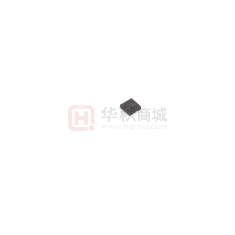
TUSB320
X2QFN (12)
1.60 mm × 1.60 mm
TUSB320I
X2QFN (12)
1.60 mm × 1.60 mm
For all available packages, see the orderable addendum at
the end of the data sheet.
VDD
(1)
VBUS
VBUS
Detection
CC Logic
For Mode
Configuration and
Detection
I2C
CC1
CC2
GPIO
Controller
GPIOs
GND
•
•
•
•
The TUSB320 device enables USB Type-C ports
with the configuration channel (CC) logic needed
for Type-C ecosystems. The TUSB320 device uses
the CC pins to determine port attach and detach,
cable orientation, role detection, and port control
for Type-C current mode. The TUSB320 device can
be configured as a downstream facing port (DFP),
upstream facing port (UFP) or a dual role port (DRP)
making it ideal for any application.
Copyright © 2016, Texas Instruments Incorporated
Simplified Schematic
Sample Applications
An IMPORTANT NOTICE at the end of this data sheet addresses availability, warranty, changes, use in safety-critical applications,
intellectual property matters and other important disclaimers. PRODUCTION DATA.
�TUSB320, TUSB320I
www.ti.com
SLLSEN9F – MAY 2015 – REVISED MARCH 2022
Table of Contents
1 Features............................................................................1
2 Applications..................................................................... 1
3 Description.......................................................................1
4 Revision History.............................................................. 2
5 Pin Configuration and Functions...................................4
6 Specifications.................................................................. 5
6.1 Absolute Maximum Ratings........................................ 5
6.2 ESD Ratings............................................................... 5
6.3 Recommended Operating Conditions.........................5
6.4 Thermal Information....................................................5
6.5 Electrical Characteristics.............................................6
6.6 Timing Requirements.................................................. 7
6.7 Switching Characteristics............................................7
7 Detailed Description........................................................9
7.1 Overview..................................................................... 9
7.2 Functional Block Diagram........................................... 9
7.3 Feature Description...................................................10
7.4 Device Functional Modes..........................................13
7.5 Programming............................................................ 15
7.6 Register Maps...........................................................16
8 Application and Implementation.................................. 20
8.1 Application Information............................................. 20
8.2 Typical Application.................................................... 21
8.3 Initialization Set Up................................................... 27
9 Power Supply Recommendations................................27
10 Layout...........................................................................27
10.1 Layout Guidelines................................................... 27
10.2 Layout Example...................................................... 27
11 Device and Documentation Support..........................28
11.1 Receiving Notification of Documentation Updates.. 28
11.2 Support Resources................................................. 28
11.3 Trademarks............................................................. 28
11.4 Electrostatic Discharge Caution.............................. 28
11.5 Glossary.................................................................. 28
12 Mechanical, Packaging, and Orderable
Information.................................................................... 28
4 Revision History
NOTE: Page numbers for previous revisions may differ from page numbers in the current version.
Changes from Revision E (May 2017) to Revision F (March 2022)
Page
• Updated the numbering format for tables, figures, and cross-references throughout the document..................1
• Updated the term master to controller throughout the data sheet to align with MIPI I3C specification and
NXP's Inclusive Language Project......................................................................................................................1
• Added the Junction Temperature to the Absolute Maximum Ratings section.....................................................5
• Changed the tCCCB_DEFAULT typical parameter from 168 ms to 133 ms.......................................................7
• Added Functional Block Diagram section........................................................................................................... 9
Changes from Revision D (October 2016) to Revision E (May 2017)
Page
• Changed RVBUS values From: MIN = 891, TYP = 900, MAX = 909 KΩ To: MIN = 855, TYP = 887, MAX = 920
KΩ ......................................................................................................................................................................6
Changes from Revision C (September 2016) to Revision D (October 2016)
Page
• Changed text for Pin 7 in the Pin Functions table From: "default current mode detected (H); medium or high
current mode detected (L)." To: "Refer to Table 7-3 for more details."............................................................... 4
• Changed text for Pin 8 in the Pin Functions table From: "default or medium current mode detected (H); high
current mode detected (L)." To: "Refer to Table 7-3 for more details."............................................................... 4
Changes from Revision B (March 2016) to Revision C (September 2016)
Page
• Changed pins CC1 and CC2 values From: MIN = -0.3 MAX = VDD + 0.3 To: MIN -0.3 MAX = 6 in the Section
6.1 ......................................................................................................................................................................5
Changes from Revision A (June 2015) to Revision B (March 2016)
Page
• Added Note 1 and 2 to the Pin Functions table.................................................................................................. 4
• Changed the DESCRIPTION of pin EN_N pin in the Pin Functions table.......................................................... 4
• Changed the DESCRIPTION of pin VDD in the Pin Functions table................................................................... 4
• Changed the MIN, TYP, and MAX values for VTH_UFP_CC_USB, VTH_UFP_CC_MED, and VTH_UFP_CC_HIGH in the
Section 6.5 table................................................................................................................................................. 6
• Added Test Condition "See Figure 6-1" to VBUS_THR in the Section 6.5 ............................................................ 6
• Added Note 2 to the Section 6.5 table ............................................................................................................... 6
2
Submit Document Feedback
Copyright © 2022 Texas Instruments Incorporated
Product Folder Links: TUSB320 TUSB320I
�TUSB320, TUSB320I
www.ti.com
•
•
•
•
•
SLLSEN9F – MAY 2015 – REVISED MARCH 2022
Updated Section 6.6 table with new values........................................................................................................ 7
Added Data hold time, Data valid time, Data valid acknowledge time, and Cbus_400kHz values to Section 6.6
table.................................................................................................................................................................... 7
Changed the Section 6.7 table .......................................................................................................................... 7
Added Note: "SW must make sure..." to the Description of INTERRUPT_STATUS in Table 7-7 .................... 16
Added text to list item 2 in the Section 8.3 section........................................................................................... 27
Changes from Revision * (May 2015) to Revision A (June 2015)
Page
• Changed device status of TUSB320 from Product Preview to Production Data ............................................... 1
Submit Document Feedback
Copyright © 2022 Texas Instruments Incorporated
Product Folder Links: TUSB320 TUSB320I
3
�TUSB320, TUSB320I
www.ti.com
SLLSEN9F – MAY 2015 – REVISED MARCH 2022
CC2
CC1
5 Pin Configuration and Functions
2
1
12
VDD
VBUS_DET
4
11
EN_N
ADDR
5
10
GND
INT_N/OUT3
6
9
ID
7
8
SCL/OUT2
3
SDA/OUT1
PORT
Figure 5-1. RWB Package, 12-Pin X2QFN (Top View)
Table 5-1. Pin Functions
PIN
NAME
NO.
TYPE(3)
DESCRIPTION
CC1
1
I/O
Type-C configuration channel signal 1
CC2
2
I/O
Type-C configuration channel signal 2
PORT(1)
3
I
Tri-level input pin to indicate port mode. The state of this pin is sampled when EN_N is asserted low and VDD is
active. This pin is also sampled following a I2C_SOFT_RESET.
H - DFP (Pull-up to VDD if DFP mode is desired)
NC - DRP (Leave unconnected if DRP mode is desired)
L - UFP (Pull-down or tie to GND if UFP mode is desired)
VBUS_DET(1)
4
I
5- to 28-V VBUS input voltage. VBUS detection determines UFP attachment. One 900-kΩ external resistor
required between system VBUS and VBUS_DET pin.
Tri-level input pin to indicate I2C address or GPIO mode:
H - I2C is enabled and I2C 7-bit address is 0x61.
ADDR(1)
5
I
NC - GPIO mode (I2C is disabled)
L - I2C is enabled and I2C 7-bit address is 0x60.
ADDR pin should be pulled up to VDD if high configuration is desired
INT_N/OUT3(1)
SDA/OUT1(1) (2)
7
O
The INT_N/OUT3 is a dual-function pin. When used as the INT_N, the pin is an open drain output in I2C control
mode and is an active low interrupt signal for indicating changes in I2C registers. When used as OUT3, the pin is
in audio accessory detect in GPIO mode: no detection (H), audio accessory connection detected (L).
I/O
The SDA/OUT1 is a dual-function pin. When I2C is enabled (ADDR pin is high or low), this pin is the I2C
communication data signal. When in GPIO mode (ADDR pin is NC), this pin is an open drain output for
communicating Type-C current mode detect when the TUSB320 device is in UFP mode: Refer to Table 7-3 for
more details.
SCL/OUT2(1) (2)
8
I/O
The SCL/OUT2 is a dual function pin. When I2C is enabled (ADDR pin is high or low), this pin is the I2C
communication clock signal. When in GPIO mode (ADDR pin is NC), this pin is an open drain output for
communicating Type-C current mode detect when the TUSB320 device is in UFP mode: Refer to Table 7-3 for
more details.
ID(1)
9
O
Open drain output; asserted low when the CC pins detect device attachment when port is a source (DFP), or
dual-role (DRP) acting as source (DFP).
GND
10
G
Ground
EN_N
11
I
Enable signal; active low. Pulled up to VDD internally to disable the TUSB320 device. If controlled externally,
must be held high at least for 50 ms after VDD has reached its valid voltage level.
VDD
12
P
Positive supply voltage. VDD must ramp within 25 ms or less
(1)
(2)
(3)
4
6
When VDD is off, the TUSB320 non-failsafe pins (VBUS_DET, ADDR, PORT, ID, OUT[3:1] pins) could back-drive the TUSB320 device
if not handled properly. When necessary to pull these pins up, it is recommended to pullup PORT, ADDR, INT_N/OUT3, and ID to the
device VDD supply. The VBUS_DET must be pulled up to VBUS through a 900-kΩ resistor.
When using the 3.3 V supply for I2C, the end user must ensure that the VDD is 3 V and above. Otherwise the I2C may back power the
device.
I = input, O = output, P = power
Submit Document Feedback
Copyright © 2022 Texas Instruments Incorporated
Product Folder Links: TUSB320 TUSB320I
�TUSB320, TUSB320I
www.ti.com
SLLSEN9F – MAY 2015 – REVISED MARCH 2022
6 Specifications
6.1 Absolute Maximum Ratings
over operating free-air temperature range (unless otherwise noted)(1)
MIN
MAX
UNIT
VDD
-0.3
6
V
PORT, ADDR, ID, EN_N, INT_N/OUT3
-0.3
VDD + 0.3
CC1, CC2
-0.3
6
SDA/OUT1, SCL/OUT2
-0.3
VDD + 0.3
VBUS_DET
-0.3
4
Storage temperature, Tstg
-65
150
°C
Junction temperature
-40
105
°C
Supply voltage
Control pins
(1)
V
Stresses beyond those listed under Absolute Maximum Ratings may cause permanent damage to the device. These are stress
ratings only, which do not imply functional operation of the device at these or any other conditions beyond those indicated under
Recommended Operating Conditions. Exposure to absolute-maximum-rated conditions for extended periods may affect device
reliability.
6.2 ESD Ratings
VALUE
V(ESD)
(1)
(2)
Electrostatic discharge
Human-body model (HBM), per ANSI/ESDA/JEDEC JS-001(1)
±7000
Charged-device model (CDM), per JEDEC specification JESD22C101(2)
±1500
UNIT
V
JEDEC document JEP155 states that 500-V HBM allows safe manufacturing with a standard ESD control process.
JEDEC document JEP157 states that 250-V CDM allows safe manufacturing with a standard ESD control process.
6.3 Recommended Operating Conditions
over operating free-air temperature range (unless otherwise noted)
MIN
VDD
Supply voltage range
2.7
VBUS
System VBUS voltage
4
VBUS_DET
VBUS_DET threshold voltage on the pin
TA
NOM
MAX
5
UNIT
5
V
28
V
4
V
TUSB320I Operating free air temperature range
–40
25
85
°C
TUSB320 Operating free air temperature range
0
25
70
°C
6.4 Thermal Information
TUSB320
THERMAL
METRIC(1)
RWB (X2QFN)
UNIT
12 PINS
RθJA
Junction-to-ambient thermal resistance
169.3
°C/W
RθJC(top)
Junction-to-case (top) thermal resistance
68.1
°C/W
RθJB
Junction-to-board thermal resistance
83.4
°C/W
ψJT
Junction-to-top characterization parameter
2.2
°C/W
ψJB
Junction-to-board characterization parameter
83.4
°C/W
RθJC(bot)
Junction-to-case (bottom) thermal resistance
N/A
(1)
For more information about traditional and new thermal metrics, see the Semiconductor and C Package Thermal Metrics application
report, SPRA953.
Submit Document Feedback
Copyright © 2022 Texas Instruments Incorporated
Product Folder Links: TUSB320 TUSB320I
5
�TUSB320, TUSB320I
www.ti.com
SLLSEN9F – MAY 2015 – REVISED MARCH 2022
6.5 Electrical Characteristics
over operating free-air temperature range (unless otherwise noted)
TEST
CONDITIONS
PARAMETER
MIN
TYP
MAX
UNIT
Power Consumption
IUNATTACHED_UFP
Current consumption in unattached mode when port is
unconnected and waiting for connection. (VDD = 4.5 V,
EN_N = L, ADDR = NC, PORT = L)
100
µA
IACTIVE_UFP
Current consumption in active mode. (VDD = 4.5 V, EN_N =
L, ADDR = NC, PORT = L)
100
µA
ISHUTDOWN
Leakage current when VDD is supplied but the TUSB320
device is not enabled. (VDD = 4.5 V, EN_N = H)
1.7
µA
CC1 and CC2 Pins
RCC_DB
Pulldown resistor when in dead-battery mode.
4.1
5.1
6.1
kΩ
RCC_D
Pulldown resistor when in UFP or DRP mode.
4.6
5.1
5.6
kΩ
VUFP_CC_USB
Voltage level range for detecting a DFP attach when
configured as an UFP and DFP is advertising default
current source capability.
0.25
0.61
V
VUFP_CC_MED
Voltage level range for detecting a DFP attach when
configured as an UFP and DFP is advertising medium (1.5
A) current source capability.
0.7
1.16
V
VUFP_CC_HIGH
Voltage level range for detecting a DFP attach when
configured as an UFP and DFP is advertising high (3 A)
current source capability.
1.31
2.04
V
VTH_DFP_CC_USB
Voltage threshold for detecting an UFP attach when
configured as a DFP and advertising default current source
capability.
1.51
1.6
1.64
V
VTH_DFP_CC_MED
Voltage threshold for detecting an UFP attach when
configured as a DFP and advertising medium current (1.5
A) source capability.
1.51
1.6
1.64
V
VTH_DFP_CC_HIGH
Voltage threshold for detecting an UFP attach when
configured as a DFP and advertising high current (3.0 A)
source capability.
2.46
2.6
2.74
V
ICC_DEFAULT_P
Default mode pullup current source when operating in DFP
or DRP mode.
64
80
96
µA
ICC_MED_P
Medium (1.5 A) mode pullup current source when operating
in DFP or DRP mode.
166
180
194
µA
ICC_HIGH_P
High (3 A) mode pullup current source when operating in
DFP or DRP mode.(1)
304
330
356
µA
0.4
V
0.56 × VDD
V
Control Pins: PORT, ADDR, INT/OUT3, EN_N, ID
6
VIL
Low-level control signal input voltage, (PORT, ADDR,
EN_N)
VIM
Mid-level control signal input voltage (PORT, ADDR)
VIH
High-level control signal input voltage (PORT, ADDR,
EN_N)
IIH
High-level input current
–20
20
IIL
Low-level input current
–10
10
REN_N
Internal pullup resistance for EN_N
1.1
Rpu (2)
Internal pullup resistance (PORT, ADDR)
588
kΩ
Rpd (2)
Internal pulldown resistance (PORT, ADDR)
1.1
MΩ
VOL
Low-level signal output voltage (open-drain) (INT_N/OUT3,
ID)
Rp_ODext
External pullup resistor on open drain IOs (INT_N/OUT3,
ID)
200
kΩ
Rp_TLext
Tri-level input external pullup resistor (PORT, ADDR)
4.7
kΩ
0.28 × VDD
VDD - 0.3
V
IOL = –1.6 mA
Submit Document Feedback
µA
µA
MΩ
0.4
V
Copyright © 2022 Texas Instruments Incorporated
Product Folder Links: TUSB320 TUSB320I
�TUSB320, TUSB320I
www.ti.com
SLLSEN9F – MAY 2015 – REVISED MARCH 2022
6.5 Electrical Characteristics (continued)
over operating free-air temperature range (unless otherwise noted)
TEST
CONDITIONS
PARAMETER
I2C
- SDA/OUT1, SCL/OUT2 can operate from 1.8 or 3.3 V
MIN
TYP
MAX
1.8
3.6
UNIT
(±10%)(3)
VDD_I2C
Supply range for I2C (SDA/OUT1, SCL/OUT2)
1.65
VIH
High-level signal voltage
1.05
VIL
Low-level signal voltage
VOL
Low-level signal output voltage (open drain)
V
V
IOL = –1.6 mA
0.4
V
0.4
V
VBUS_DET IO Pins (Connected to System VBUS signal)
VBUS_THR
VBUS threshold range
RVBUS
External resistor between VBUS and VBUS_DET pin
RVBUS_PD
Internal pulldown resistance for VBUS_DET
(1)
(2)
(3)
See Figure 6-1
2.95
3.30
3.80
V
855
887
920
KΩ
95
KΩ
VDD must be 3.5 V or greater to advertise 3 A current.
Internal pullup and pulldown for PORT and ADDR are removed after the device has sampled EN = high or EN_N = low.
When using 3.3 V for I2C, customer must ensure VDD is above 3.0 V at all times.
6.6 Timing Requirements
MIN
NOM
MAX
UNIT
I2C (SDA, SCL)
tSU:DAT
Data setup time
100
ns
tHD;DAT
Data hold time
10
ns
tSU:STA
Set-up time, SCL to start condition
0.6
µs
tHD:STA
Hold time, (repeated) start condition to SCL
0.6
µs
tSU:STO
Set up time for stop condition
0.6
µs
tBUF
Bus free time between a stop and start condition
1.3
µs
tVD;DAT
Data valid time
0.9
ns
tVD;ACK
Data valid acknowledge time
0.9
ns
I2C
mode for local
I2C
fSCL
SCL clock frequency;
400
kHz
tr
Rise time of both SDA and SCL signals
control
300
ns
tf
Fall time of both SDA and SCL signals
300
ns
Cbus_100kHz
Total capacitive load for each bus line when operating at ≤ 100 kHz
400
pF
Cbus_400kHz
Total capacitive load for each bus line when operating at ≤ 400 kHz
100
pF
MAX
UNIT
6.7 Switching Characteristics
over operating free-air temperature range (unless otherwise noted)
PARAMETER
TEST CONDITIONS
tCCCB_DEFAULT
Power on default of CC1 and CC2 voltage debounce
time
tVBUS_DB
Debounce of VBUS_DET pin after valid VBUS_THR
tDRP_DUTY_CYCLE
Power-on default of percentage of time DRP
advertises DFP during a tDRP
tDRP
The period during which the TUSB320 or the
TUSB320I in DFP mode completes a DFP to UFP
and back advertisement.
tI2C_EN
Time from TUSB320 EN_N low or TUSB320I EN high
and VDD active to I2C access available
tSOFT_RESET
Soft reset duration
MIN
DEBOUCE
register = 2'b00
DRP_DUTY_CYCLE
register = 2'b00
TYP
133
ms
2
ms
30%
50
26
75
49
100
ms
100
ms
95
ms
Submit Document Feedback
Copyright © 2022 Texas Instruments Incorporated
Product Folder Links: TUSB320 TUSB320I
7
�TUSB320, TUSB320I
www.ti.com
SLLSEN9F – MAY 2015 – REVISED MARCH 2022
VBUS
VBUS_THR
TVBUS_DB
0V
Figure 6-1. VBUS Detect and Debounce
8
Submit Document Feedback
Copyright © 2022 Texas Instruments Incorporated
Product Folder Links: TUSB320 TUSB320I
�TUSB320, TUSB320I
www.ti.com
SLLSEN9F – MAY 2015 – REVISED MARCH 2022
7 Detailed Description
7.1 Overview
The USB Type-C ecosystem operates around a small form factor connector and cable that is flippable and
reversible. Because of the nature of the connector, a scheme is needed to determine the connector orientation.
Additional schemes are needed to determine when a USB port is attached and the acting role of the USB port
(DFP, UFP, and DRP), as well as to communicate Type-C current capabilities. These schemes are implemented
over the CC pins according to the USB Type-C specifications. The TUSB320 device provides Configuration
Channel (CC) logic for determining USB port attach and detach, role detection, cable orientation, and Type-C
current mode. The TUSB320 device also contains several features such as mode configuration and low standby
current which make this device ideal for source or sinks in USB 2.0 applications.
VDD
7.2 Functional Block Diagram
ADDR
3-State Buffer
PORT
CC1
Connection and
cable detection
VBUS_ON
CTRL_EN_N
SCL/OUT2
Open Drain
Output
CTRL_EN
ID
VBUS Detection
SYS_VBUS
VBUS_DET
INT/OUT3
EN_N Logic
GND
EN_N
VBUS_ON
CSR
CTRL_ID
I2C
CC2
CTRL_INT
SDA/OUT1
CTRL_ID
CTRL_INT
Digital Controller
900 K ±1%
Copyright © 2016, Texas Instruments Incorporated
Figure 7-1. Functional Block Diagram of TUSB320
7.2.1 Cables, Adapters, and Direct Connect Devices
Type-C Specification 1.1 defines several cables, plugs and receptacles to be used to attach ports. The TUSB320
device supports all cables, receptacles, and plugs. The TUSB320 device does not support e-marking.
7.2.1.1 USB Type-C Receptacles and Plugs
Below is list of Type-C receptacles and plugs supported by the TUSB320 device:
•
•
•
USB Type-C receptacle for USB 2.0 platforms and devices
USB full-featured Type-C plug
USB 2.0 Type-C plug
Submit Document Feedback
Copyright © 2022 Texas Instruments Incorporated
Product Folder Links: TUSB320 TUSB320I
9
�TUSB320, TUSB320I
www.ti.com
SLLSEN9F – MAY 2015 – REVISED MARCH 2022
7.2.1.2 USB Type-C Cables
Below is a list of Type-C cable types supported by the TUSB320 device:
•
•
•
USB full-featured Type-C cable
USB 2.0 Type-C cable with USB 2.0 plug
Captive cable with either a USB full-featured plug or USB 2.0 plug
7.2.1.3 Legacy Cables and Adapters
The TUSB320 device supports legacy cable adapters as defined by the Type-C specification. The cable adapter
must correspond to the mode configuration of the TUSB320 device.
To System VBUS detection
VBUS
900 kΩ ± 1%
Rp (56k ± 5%)
VBUS_DET
TUSB320
CC
CC
Rd (5.1k ± 10%)
Legacy Host Adapter
Copyright © 2016, Texas Instruments Incorporated
Figure 7-2. Legacy Adapter Implementation Circuit
7.2.1.4 Direct Connect Devices
The TUSB320 device supports the attaching and detaching of a direct-connect device.
7.2.1.5 Audio Adapters
Additionally, the TUSB320 device supports audio adapters for audio accessory mode, including:
•
•
Passive audio adapter
Charge through audio adapter
7.3 Feature Description
7.3.1 Port Role Configuration
The TUSB320 device can be configured as a downstream facing port (DFP), upstream facing port (UFP), or
dualrole port (DRP) using the tri-level PORT pin. The PORT pin should be pulled high to VDD using a pullup
resistance, low to GND or left as floated on the PCB to achieve the desired mode. This flexibility allows the
TUSB320 device to be used in a variety of applications. The TUSB320 device samples the PORT pin after reset
and maintains the desired mode until the TUSB320 device is reset again. Table 7-1 lists the supported features
in each mode.
10
Submit Document Feedback
Copyright © 2022 Texas Instruments Incorporated
Product Folder Links: TUSB320 TUSB320I
�TUSB320, TUSB320I
www.ti.com
SLLSEN9F – MAY 2015 – REVISED MARCH 2022
Table 7-1. Supported Features for the TUSB320 Device by Mode
PORT PIN
HIGH
(DFP ONLY)
LOW
(UFP ONLY)
NC
(DRP)
Port attach and
detach
Yes
Yes
Yes
Cable orientation
(through I2C)
Yes
Yes
Yes
Current
advertisement
Yes
—
Yes (DFP)
SUPPORTED
FEATURES
Current detection
—
Yes
Yes (UFP)
Accessory modes
(audio and debug)
Yes
—
Yes
Active cable detection
Yes
—
Yes (DFP)
I2C
Yes
Yes
Yes
Legacy cables
/ GPIO
Yes
Yes
Yes
VBUS detection
—
Yes
Yes (UFP)
7.3.1.1 Downstream Facing Port (DFP) – Source
The TUSB320 device can be configured as a DFP only by pulling the PORT pin high through a resistance to
VDD. In DFP mode, the TUSB320 device constantly presents Rps on both CC. In DFP mode, the TUSB320
device initially advertises default USB Type-C current. The Type-C current can be adjusted through I2C if the
system needs to increase the amount advertised. The TUSB320 device adjusts the Rps to match the desired
Type-C current advertisement. In GPIO mode, the TUSB320 device only advertises default Type-C current.
When configured as a DFP, the TUSB320 can operate with older USB Type-C 1.0 devices except for a USB
Type-C 1.0 DRP device. The TUSB320 can not operate with a USB Type-C 1.0 DRP device. This limitation is a
result of a backwards compatibility problem between USB Type-C 1.1 DFP and a USB Type-C 1.0 DRP.
7.3.1.2 Upstream Facing Port (UFP) – Sink
The TUSB320 device can be configured as an UFP only by pulling the PORT pin low to GND. In UFP mode, the
TUSB320 device constantly presents pulldown resistors (Rd) on both CC pins. The TUSB320 device monitors
the CC pins for the voltage level corresponding to the Type-C mode current advertisement by the connected
DFP. The TUSB320 device debounces the CC pins and wait for VBUS detection before successfully attaching. As
an UFP, the TUSB320 device detects and communicates the advertised current level of the DFP to the system
through the OUT1 and OUT2 GPIOs (if in GPIO mode) or through the I2C CURRENT_MODE_DETECT register
one time in the Attached.SNK state.
After initial connection, the advertised current by the connected DFP could change due to changes in its system
power resource. For example, a DFP could advertise high current on initial connection but then decide to reduce
to default current because user removed external power adapter from their notebook. Because the TUSB320
will only advertise on OUT1 and OUT2 the initial advertised current, it is recommend to monitor the advertised
current through the TUSB320’s I2C interface from the CURRENT_MODE_DETECT register. System software
must periodically perform a I2C_SOFT_RESET in order for the CURRENT_MODE_DETECT register to be
updated based on the state of the CC pins.
7.3.1.3 Dual Role Port (DRP)
The TUSB320 device can be configured to operate as a DRP when the PORT pin is left floated on the PCB. In
DRP mode, the TUSB320 device toggles between operating as a DFP and an UFP. When functioning as a DFP
in DRP mode, the TUSB320 device complies with all operations as defined for a DFP according to the Type-C
specification. When presenting as an UFP in DRP mode, the TUSB320 device operates as defined for an UFP
according to the Type-C specification.
Submit Document Feedback
Copyright © 2022 Texas Instruments Incorporated
Product Folder Links: TUSB320 TUSB320I
11
�TUSB320, TUSB320I
www.ti.com
SLLSEN9F – MAY 2015 – REVISED MARCH 2022
7.3.2 Type-C Current Mode
When a valid cable detection and attach have been completed, the DFP has the option to advertise the level of
Type-C current an UFP can sink. The default current advertisement for the TUSB320 device is 500 mA (for USB
2.0) or 900 mA (for USB 3.1). If a higher level of current is available, the I2C registers can be written to provide
medium current at 1.5 A or high current at 3 A. When the CURRENT_MODE_ADVERTISE register has been
written to advertise higher than default current, the DFP adjusts the Rps for the specified current level. If a DFP
advertises 3 A, it ensures that the VDD of the TUSB320 device is 3.5 V or greater. Table 7-2 lists the Type-C
current advertisements in GPIO an I2C modes.
Table 7-2. Type-C Current Advertisement for GPIO and I2C Modes
Default
500 mA (USB
2.0)
900 mA (USB
3.1)
Medium – 1.5 A
I2C MODE (ADDR PIN H, L)
GPIO MODE (ADDR PIN IN NC)
TYPE-C CURRENT
UFP (PORT PIN L)
Current mode detected
and output through
OUT1 / OUT2
High – 3 A
DFP (PORT PIN H)
Only advertisement
UFP
Current mode detected
and read through I2C
register
N/A
DFP
I2C register default is 500
or 900 mA
Advertisement selected
through writing I2C register
7.3.3 Accessory Support
The TUSB320 device supports audio and debug accessories in DFP mode and DRP mode. Audio and debug
accessory support is provided through reading of I2C registers. Audio accessory is also supported through GPIO
mode with INT_N/OUT3 pin (audio accessory is detected when INT_N/OUT3 pin is low).
7.3.3.1 Audio Accessory
Audio accessory mode is supported through two types of adapters. First, the passive audio adapter can be used
to convert the Type-C connector into an audio port. To effectively detect the passive audio adapter, the TUSB320
device must detect a resistance < Ra on both of the CC pins.
Secondly, a charge through audio adapter may be used. The primary difference between a passive and charge
through adapter is that the charge through adapter supplies 500 mA of current over VBUS. The charge through
adapter contains a receptacle and a plug. The plug acts as a DFP and supply VBUS when the plug detects a
connection.
When the TUSB320 device is configured in GPIO mode, OUT3 pin determines if an audio accessory is
connected. When an audio accessory is detected, the OUT3 pin is pulled low.
7.3.3.2 Debug Accessory
Debug is an additional state supported by USB Type-C. The specification does not define a specific user
scenario for this state, but it is important because the end user could use debug accessory mode to enter a test
state for production specific to the application. Charge through debug accessory is not supported by TUSB320
when in DRP or UFP mode.
7.3.4 I2C and GPIO Control
The TUSB320 device can be configured for I2C communication or GPIO outputs using the ADDR pin. The ADDR
pin is a tri-level control pin. When the ADDR pin is left floating (NC), the TUSB320 device is in GPIO output
mode. When the ADDR pin is pulled high or pulled low, the TUSB320 device is in I2C mode.
All outputs for the TUSB320 device are open drain configuration.
The OUT1 and OUT2 pins are used to output the Type-C current mode when in GPIO mode. Additionally, the
OUT3 pin is used to communicate the audio accessory mode in GPIO mode. Table 7-3 lists the output pin
settings. See the Pin Functions table for more information.
12
Submit Document Feedback
Copyright © 2022 Texas Instruments Incorporated
Product Folder Links: TUSB320 TUSB320I
�TUSB320, TUSB320I
www.ti.com
SLLSEN9F – MAY 2015 – REVISED MARCH 2022
Table 7-3. Simplified Operation for OUT1 and OUT2
OUT1
OUT2
ADVERTISEMENT
H
H
Default Current in Unattached State
H
L
Default Current in Attached State
L
H
Medium Current (1.5 A) in Attached State
L
L
High Current (3.0 A) in Attached State
When operating in I2C mode, the TUSB320 device uses the SCL and SDA lines for clock and data and
the INT_N pin to communicate a change in I2C registers, or an interrupt, to the system. The INT_N pin is
pulled low when the TUSB320 device updates the registers with new information. The INT_N pin is open
drain. The INTERRUPT_STATUS register should be set when the INT_N pin is pulled low. To clear the
INTERRUPT_STATUS register, the end user writes to I2C.
When operating in GPIO mode, the OUT3 pin is used in place of the INT_N pin to determine if an audio
accessory is detected and attached. The OUT3 pin is pulled low when an audio accessory is detected.
Note
I2C,
When using the 3.3 V supply for
the end user must ensure that the VDD is 3 V and above.
Otherwise the I2C may back power the device.
7.3.5 VBUS Detection
The TUSB320 device supports VBUS detection according to the Type-C specification. VBUS detection is used to
determine the attachment and detachment of an UFP and to determine the entering and exiting of accessary
modes. VBUS detection is also used to successfully resolve the role in DRP mode.
The system VBUS voltage must be routed through a 900-kΩ resistor to the VBUS_DET pin on the TUSB320
device if the PORT pin is configured as a DRP or an UFP. If the TUSB320 device is configured as a DFP and
only ever used in DFP mode, the VBUS_DET pin can be left unconnected.
7.4 Device Functional Modes
The TUSB320 device has four functional modes. Table 7-4 lists these modes:
Table 7-4. USB Type-C States According to TUSB320 Functional Modes
MODES
GENERAL BEHAVIOR
STATES(1)
PORT PIN
Unattached.SNK
UFP
Unattached
USB port unattached. ID, PORT
operational. I2C on. CC pins
configure according to PORT pin.
DRP
AttachWait.SNK
Toggle Unattached.SNK → Unattached.SRC
AttachedWait.SRC or AttachedWait.SNK
Unattached.SRC
DFP
AttachWait.SRC
UFP
Attached.SNK
Attached.SNK
Attached.SRC
DRP
Active
Audio accessory
USB port attached. All GPIOs
operational. I2C on.
Debug accessory
Attached.SRC
DFP
Audio accessory
Debug accessory
Dead battery
No operation.
VDD not available.
UFP/DRP/DFP
Default device state to UFP/SNK with Rd.
Submit Document Feedback
Copyright © 2022 Texas Instruments Incorporated
Product Folder Links: TUSB320 TUSB320I
13
�TUSB320, TUSB320I
www.ti.com
SLLSEN9F – MAY 2015 – REVISED MARCH 2022
Table 7-4. USB Type-C States According to TUSB320 Functional Modes (continued)
(1)
MODES
GENERAL BEHAVIOR
PORT PIN
STATES(1)
Shutdown
VDD available.
EN_N pin high.
UFP/DRP/DFP
Default device state to UFP/SNK with Rd.
Required; not in sequential order.
7.4.1 Unattached Mode
Unattached mode is the primary mode of operation for the TUSB320 device, because a USB port can be
unattached for a lengthy period of time. In unattached mode, VDD is available, and all IOs and I2C are
operational. After the TUSB320 device is powered up, the part enters unattached mode until a successful attach
has been determined. Initially, right after power up, the TUSB320 device comes up as an Unattached.SNK. The
TUSB320 device checks the PORT pin and operates according to the mode configuration. The TUSB320 device
toggles between the UFP and the DFP if configured as a DRP. In unattached mode, I2C can be used to change
the mode configuration or port role if the board configuration of the PORT pin is not the desired mode. Writing
to the I2C MODE_SELECT register can override the PORT pin only in unattached mode. The PORT pin is only
sampled at reset or power up. I2C must be used after reset to change the device mode configuration.
7.4.2 Active Mode
Active mode is defined as the port being attached. In active mode, all GPIOs are operational, and I2C is read /
write (R/W). When in active mode, the TUSB320 device communicates to the AP that the USB port is attached.
This happens through the ID pin if TUSB320 is configured as a DFP or DRP connect as source. If TUSB320
is configured as an UFP or a DRP connected as a sink, the OUT1/OUT2 and INT_N/OUT3 pins are used. The
TUSB320 device exits active mode under the following conditions:
•
•
•
•
Cable unplug
VBUS removal if attached as an UFP
Dead battery; system battery or supply is removed
EN_N pin floated or pulled high
During active mode, I2C cannot be used to change the mode configuration. This can only be done if TUSB320 is
in an unattached state.
7.4.3 Dead Battery Mode
During dead battery mode, VDD is not available. CC pins always default to pulldown resistors in dead battery
mode. Dead battery mode means:
•
•
TUSB320 in UFP with 5.1-kΩ ± 20% Rd; cable connected and providing charge
TUSB320 in UFP with 5.1-kΩ ± 20% Rd; nothing connected (application could be off or have a discharged
battery)
Upon exiting dead battery mode (VDD is active), the software must perform the following sequence in order for
Rp to be presented on both CC pins:
1. Write a 0x04 to I2C address 0x45.
2. Wait 30ms.
3. Write a 0x00 to I2C address 0x45.
Between steps 1 and 3, the status flags will be set. The software must ignore these flags when performing the
three steps.
Note
When VDD is off, the TUSB320 non-failsafe pins ( VBUS_DET, ADDR, PORT, ID, OUT[3:1] pins)
could back-drive the TUSB320 device if not handled properly. When necessary to pull these pins up,
it is recommended to pullup PORT, ADDR, INT_N/OUT3, and ID to the device’s VDD supply. The
VBUS_DET must be pulled up to VBUS through a 900-kΩ resistor.
14
Submit Document Feedback
Copyright © 2022 Texas Instruments Incorporated
Product Folder Links: TUSB320 TUSB320I
�TUSB320, TUSB320I
www.ti.com
SLLSEN9F – MAY 2015 – REVISED MARCH 2022
7.4.4 Shutdown Mode
Shutdown mode for TUSB320 device is defined as follows:
•
•
•
Supply voltage available and EN_N pin is pulled high.
EN_N pin has internal pullup resistor.
The TUSB320 device is off, but still maintains the Rd on the CC pins.
7.5 Programming
For further programmability, the TUSB320 device can be controlled using I2C. The TUSB320 device local
I2C interface is available for reading/writing after TI2C_EN when the device is powered up. The SCL and SDA
terminals are used for I2C clock and I2C data respectively. If I2C is the preferred method of control, the ADDR pin
must be set accordingly.
Table 7-5. TUSB320 I2C Addresses
TUSB320 I2C Target Address
ADDR pin
Bit 7 (MSB)
Bit 6
Bit 5
H
1
1
0
Bit 4
0
Bit 3
0
Bit 2
0
Bit 1
1
Bit 0 (W/R)
0/1
L
1
1
0
0
0
0
0
0/1
The following procedure should be followed to write to TUSB320 I2C registers:
1. The controller initiates a write operation by generating a start condition (S), followed by the TUSB320 7-bit
address and a zero-value R/W bit to indicate a write cycle
2. The TUSB320 device acknowledges the address cycle
3. The controller presents the sub-address (I2C register within the TUSB320 device) to be written, consisting of
one byte of data, MSB-first
4. The TUSB320 device acknowledges the sub-address cycle
5. The controller presents the first byte of data to be written to the I2C register
6. The TUSB320 device acknowledges the byte transfer
7. The controller may continue presenting additional bytes of data to be written, with each byte transfer
completing with an acknowledge from the TUSB320 device
8. The controller terminates the write operation by generating a stop condition (P)
The following procedure should be followed to read the TUSB320 I2C registers:
1. The controller initiates a read operation by generating a start condition (S), followed by the TUSB320 7-bit
address and a one-value R/W bit to indicate a read cycle
2. The TUSB320 device acknowledges the address cycle
3. The TUSB320 device transmits the contents of the memory registers MSB-first starting at register 00h or
last read sub-address+1. If a write to the T I2C register occurred prior to the read, then the TUSB320 device
starts at the sub-address specified in the write.
4. The TUSB320 device waits for either an acknowledge (ACK) or a not-acknowledge (NACK) from the
controller after each byte transfer; the I2C controller acknowledges reception of each data byte transfer
5. If an ACK is received, the TUSB320 device transmits the next byte of data
6. The controller terminates the read operation by generating a stop condition (P)
The following procedure should be followed for setting a starting sub-address for I2C reads:
1. The controller initiates a write operation by generating a start condition (S), followed by the TUSB320 7-bit
address and a zero-value R/W bit to indicate a read cycle
2. The TUSB320 device acknowledges the address cycle
3. The controller presents the sub-address (I2C register within the TUSB320 device) to be read, consisting of
one byte of data, MSB-first
4. The TUSB320 device acknowledges the sub-address cycle
5. The controller terminates the read operation by generating a stop condition (P)
Submit Document Feedback
Copyright © 2022 Texas Instruments Incorporated
Product Folder Links: TUSB320 TUSB320I
15
�TUSB320, TUSB320I
www.ti.com
SLLSEN9F – MAY 2015 – REVISED MARCH 2022
Note
If no sub-addressing is included for the read procedure, then the reads start at register offset 00h and
continue byte-by-byte through the registers until the I2C controller terminates the read operation. If a
I2C address write occurred prior to the read, then the reads start at the sub-address specified by the
address write.
7.6 Register Maps
Table 7-6. CSR Registers
ACCESS
TAG
NAME
R
Read
The field may be read by software.
W
Write
The field may be written by software.
MEANING
S
Set
The field may be set by a write of one. Writes of zeros to the field have no effect.
C
Clear
The field may be cleared by a write of one. Writes of zeros to the field have no effect.
U
Update
Hardware may autonomously update this field.
NA
No Access
Not accessible or not applicable.
Table 7-7. CSR Registers Bit Address and Description
16
ADDRESS
BIT(S)
BIT NAME
DESCRIPTION
0x00 – 0x07
7:0
DEVICE_ID
For the TUSB320 device these fields return a string of
ASCII characters returning TUSB320
Addresses 0x07 - 0x00 = {0x00 0x54 0x55 0x53 0x42 0x33
0x32 0x30}
Submit Document Feedback
ACCESS
R
Copyright © 2022 Texas Instruments Incorporated
Product Folder Links: TUSB320 TUSB320I
�TUSB320, TUSB320I
www.ti.com
SLLSEN9F – MAY 2015 – REVISED MARCH 2022
Table 7-7. CSR Registers Bit Address and Description (continued)
ADDRESS
BIT(S)
BIT NAME
DESCRIPTION
ACCESS
These bits are programmed by the application to raise the
current advertisement from default.
00 – Default (500 mA / 900 mA) initial value at startup
7:6
CURRENT_MODE_ADVERTISE
RW
01 – Medium (1.5 A)
10 – High (3 A)
11 – Reserved
These bits are set when an UFP determines the Type-C
Current mode.
00 – Default (value at start up)
5:4
CURRENT_MODE_DETECT
RU
01 – Medium
10 – Charge through accessory – 500 mA
11 – High
0x08
These bits are read by the application to determine if an
accessory was attached.
000 – No accessory attached (default)
001 – Reserved
010 – Reserved
3:1
ACCESSORY_CONNECTED
RU
011 – Reserved
100 – Audio accessory
101 – Audio charged thru accessory
110 – Debug accessory
111 – Reserved
0
ACTIVE_CABLE_DETECTION
This flag indicates that an active cable has been plugged
into the Type-C connector. When this field is set, an active
cable is detected.
RU
Submit Document Feedback
Copyright © 2022 Texas Instruments Incorporated
Product Folder Links: TUSB320 TUSB320I
17
�TUSB320, TUSB320I
www.ti.com
SLLSEN9F – MAY 2015 – REVISED MARCH 2022
Table 7-7. CSR Registers Bit Address and Description (continued)
ADDRESS
BIT(S)
BIT NAME
DESCRIPTION
ACCESS
This is an additional method to communicate attach other
than the ID pin. These bits can be read by the application to
determine what was attached.
7:6
00 – Not attached (default)
ATTACHED_STATE
RU
01 – Attached.SRC (DFP)
10 – Attached.SNK (UFP)
11 – Attached to an accessory
Cable orientation. The application can read these bits for
cable orientation information.
5
CABLE_DIR
RU
0 – CC1
1 – CC2 (default)
The INT pin is pulled low whenever a CSR changes. When
a CSR change has occurred this bit should be held at 1 until
the application clears it.
0x09
0 – Clear
4
INTERRUPT_STATUS
1 – Interrupt (When INT_N is pulled low, this bit will be 1.
This bit is 1 whenever any CSR are changed)
RCU
Note: SW must make sure the INTERRUPT_STATUS has
been cleared to zero. Rewrites to this register are needed
for the INT_N to be correctly asserted for all interrupt
events.
3
Reserved
R
Percentage of time that a DRP advertises DFP during tDRP
00 – 30% (default)
2:1
DRP_DUTY_CYCLE
01 – 40%
RW
10 – 50%
11 – 60%
0
18
Reserved
Submit Document Feedback
R
Copyright © 2022 Texas Instruments Incorporated
Product Folder Links: TUSB320 TUSB320I
�TUSB320, TUSB320I
www.ti.com
SLLSEN9F – MAY 2015 – REVISED MARCH 2022
Table 7-7. CSR Registers Bit Address and Description (continued)
ADDRESS
BIT(S)
BIT NAME
DESCRIPTION
ACCESS
The nominal amount of time the TUSB320 device
debounces the voltages on the CC pins.
00 – 133 ms (default)
7:6
DEBOUNCE
RW
01 – 116 ms
10 – 151 ms
11 – 168 ms
This register can be written to set the TUSB320 device
mode operation. The ADDR pin must be set to I2C
mode. If the default is maintained, the TUSB320 device
operates according to the PORT pin levels and modes.
The MODE_SELECT can only be changed when in the
unattached state.
5:4
MODE_SELECT
0x0A
00 – Maintain mode according to PORT pin selection
(default)
RW
01 – UFP mode (unattached.SNK)
10 – DFP mode (unattached.SRC)
11 – DRP mode (start from unattached.SNK)
This resets the digital logic. The bit is self-clearing. A write
of 1 starts the reset. The following registers maybe affected
after setting this bit:
CURRENT_MODE_DETECT
3
I2C_SOFT_RESET
RSU
ACTIVE_CABLE_DETECTION
ACCESSORY_CONNECTED
ATTACHED_STATE
CABLE_DIR
2:1
Reserved
R
0
Reserved
R
7:3
Reserved
R
When this field is set, Rd and Rp are disabled.
0x45
2
DISABLE_RD_RP
0 – Normal operation (default)
RW
1 – Disable Rd and Rp
1:0
Reserved. For TI internal use only. Do not change default
value.
RW
Submit Document Feedback
Copyright © 2022 Texas Instruments Incorporated
Product Folder Links: TUSB320 TUSB320I
19
�TUSB320, TUSB320I
www.ti.com
SLLSEN9F – MAY 2015 – REVISED MARCH 2022
8 Application and Implementation
Note
Information in the following applications sections is not part of the TI component specification, and
TI does not warrant its accuracy or completeness. TI’s customers are responsible for determining
suitability of components for their purposes. Customers should validate and test their design
implementation to confirm system functionality.
8.1 Application Information
The TUSB320 device is a Type-C configuration channel logic and port controller. The TUSB320 device can
detect when a Type-C device is attached, what type of device is attached, the orientation of the cable, and power
capabilities (both detection and broadcast). The TUSB320 device can be used in a source application (DFP) or
in a sink application (UFP).
VBUS
5V
VBUS
PMIC
VPH
VDD
CC1
CC/Mode
Controller
PORT
Processor
CC2
GPIOs
DP
I2C
DM
PORT
VBUS
CC1
VDD
CC/Mode
Controller
ID
DP
GPIOs
Processor
DM
I2C
GND
TUSB320
TUSB320
Copyright © 2016, Texas Instruments Incorporated
Figure 8-1. TUSB320 in UFP Mode Supporting
Default Implementation
Legacy TypeA
Switch
5V
VBUS
Copyright © 2016, Texas Instruments Incorporated
Figure 8-2. TUSB320 in UFP Mode Supporting
Advanced Power Delivery
VBUS
PMIC
VDD
PORT
VPH
VDD
CC1
PORT
Processor
CC/Mode
Controller
CC2
DP
GPIOs
DM
I2C
VBUS
VDD
CC1
CC/Mode
Controller
ID
Processor
DM
I2C
TUSB320
TUSB320
Copyright © 2016, Texas Instruments Incorporated
Figure 8-3. TUSB320 in DFP Mode Supporting
Default Implementation
Legacy TypeA
Switch
5V
VBUS
Copyright © 2016, Texas Instruments Incorporated
Figure 8-4. TUSB320 in DFP Mode Supporting
Advanced Power Delivery
VBUS
PMIC
VPH
VDD
CC1
CC/Mode
Controller
PORT
Processor
CC2
DP
GPIOs
DM
I2C
PORT
VBUS
VDD
Processor
CC/Mode
Controller
CC2
DP
GPIOs
DM
I2C
TUSB320
TUSB320
Copyright © 2016, Texas Instruments Incorporated
Figure 8-5. TUSB320 in DRP Mode Supporting
Default Implementation
20
CC1
ID
USB TypeC Port
VBUS
USB TypeC Port
ID
2.7 - 5 V
CC2
DP
GPIOs
USB TypeC Port
VBUS
USB TypeC Port
ID
VDD
2.7 - 5 V
CC2
USB TypeC Port
2.7 - 5 V
VBUS
USB TypeC Port
ID
Copyright © 2016, Texas Instruments Incorporated
Figure 8-6. TUSB320 in DRP Mode Supporting
Advanced Power Delivery
Submit Document Feedback
Copyright © 2022 Texas Instruments Incorporated
Product Folder Links: TUSB320 TUSB320I
�TUSB320, TUSB320I
www.ti.com
SLLSEN9F – MAY 2015 – REVISED MARCH 2022
8.2 Typical Application
8.2.1 DRP in I2C Mode
Figure 8-7 shows the TUSB320 device configured as a DRP in I2C mode.
USB VBUS Switch
(optional BC 1.2 support for legacy)
SCL
SDA
DM
DP
DM_OUT
DM_IN
DP_OUT
DP_IN
VIN
EN
VOUT
System VBUS
PS_EN
Disconnect
bulk cap
when UFP
FAULT#
PS_FAULT#
VBUS
I2C I/O
1.8 V or 3.3 V
VBAT
USB2
OTG &
PMIC
150 uF
DM
100 nF
DP
VBUS
200 K
200 K
900 K
A1
VBUS_DET
PORT
INT_N/OUT3
TUSB320
SCL/OUT2
SDA/OUT1
CC1
CC2
GND
SCL
SDA
CC2
EN_N
ID
ID
CC1
ADDR
INT#
1 uF
B12
A2
B11
A3
B10
A4
B9
A5
B8
A6
B7
A7
B6
A8
B5
A9
B4
A10
B3
A11
B2
A12
B1
Type C
Receptacle
4.7 K
VDD
4.7 K
Copyright © 2016, Texas Instruments Incorporated
Figure 8-7. DRP in I2C Mode Schematic
8.2.1.1 Design Requirements
For this design example, use the parameters listed in Table 8-1:
Table 8-1. Design Requirements for DRP in I2C Mode
DESIGN PARAMETER
VALUE
VDD (2.75 V to 5 V)
VBAT (less than 5 V)
Mode (I2C or GPIO)
I2C
ADDR pin must be pulled down or pulled up
I2C address (0x61 or 0x60)
0x60
ADDR pin must be pulled low or tied to GND
Type-C port type (UFP, DFP, or DRP)
DRP
PORT pin is NC
Shutdown support (EN_N control)
No
8.2.1.2 Detailed Design Procedure
The TUSB320 device supports a VDD in the range of 2.75 V to 5 V. In this particular use case, VBAT which must
be in the required VDD range is connected to the VDD pin. A 100-nF capacitor is placed near VDD.
The TUSB320 device is placed into I2C mode by either pulling the ADDR pin high or low. In this case, the ADDR
pin is tied to GND which results in a I2C address of 0x60. The SDA and SCL must be pulled up to either 1.8 V or
3.3 V. When pulled up to 3.3 V, the VDD supply must be at least 3 V to keep from back-driving the I2C interface.
The TUSB320 device can enter shutdown mode by pulling the EN_N pin high, which puts the TUSB320 device
into a low power state. In this case, external control of the EN_N pin is not implemented and therefore the EN_N
pin is tied to GND.
Submit Document Feedback
Copyright © 2022 Texas Instruments Incorporated
Product Folder Links: TUSB320 TUSB320I
21
�TUSB320, TUSB320I
www.ti.com
SLLSEN9F – MAY 2015 – REVISED MARCH 2022
The INT_N/OUT3 pin is used to notify the PMIC when a change in the TUSB320 I2C registers occurs. This pin is
an open drain output and requires an external pullup resistor. The pin should be pulled up to VDD using a 200-kΩ
resistor.
The ID pin is used to indicate when a connection has occurred if the TUSB320 device is a DFP while configured
for DRP. An OTG USB controller can use this pin to determine when to operate as a USB host or USB device.
When this pin is driven low, the OTG USB controller functions as a host and then enables VBUS. The Type-C
standard requires that a DFP should not enable VBUS until it is in the Attached.SRC state. If the ID pin is not
low but VBUS is detected, then OTG USB controller functions as a device. The ID pin is open drain output and
requires an external pullup resistor. It should be pulled up to VDD using a 200-kΩ resistor.
The Type-C port mode is determined by the state of the PORT pin. When the PORT pin is not connected, the
TUSB320 device is in DRP mode. The Type-C port mode can also be controlled by the MODE_SELECT register
through the I2C interface when the TUSB320 device is in the unattached state.
The VBUS_DET pin must be connected through a 900-kΩ resistor to VBUS on the Type-C that is connected. This
large resistor is required to protect the TUSB320 device from large VBUS voltage that is possible in present day
systems. This resistor along with internal pulldown keeps the voltage observed by the TUSB320 device in the
recommended range.
The USB2 specification requires the bulk capacitance on VBUS based on UFP or DFP. When operating the
TUSB320 device in a DRP mode, it alternates between UFP and DFP. If the TUSB320 device connects as an
UFP, the large bulk capacitance must be removed. The FET in Figure 8-7 performs this task.
Table 8-2. USB2 Bulk Capacitance Requirements
PORT CONFIGURATION
MIN
Downstream facing port (DFP)
120
Upstream facing port (UFP)
1
MAX
UNIT
µF
10
µF
8.2.1.3 Application Curves
Figure 8-8. Application Curve for DRP in I2C Mode
22
Submit Document Feedback
Copyright © 2022 Texas Instruments Incorporated
Product Folder Links: TUSB320 TUSB320I
�TUSB320, TUSB320I
www.ti.com
SLLSEN9F – MAY 2015 – REVISED MARCH 2022
8.2.2 DFP in I2C Mode
Figure 8-9 shows the TUSB320 device configured as a DFP in I2C mode.
USB VBUS Switch
(optional BC 1.2 support for legacy)
SCL
SDA
DM
DP
DM_OUT
DM_IN
DP_OUT
DP_IN
VIN
EN
FAULT#
VOUT
System VBUS
PS_EN
PS_FAULT#
I2C I/O
1.8 V or 3.3 V
VDD_5 V
USB2
Host &
PMIC
150 uF
100 nF
DM
DP
VBUS
200 K
200 K
4.7 K
A1
VBUS_DET
PORT
INT_N/OUT3
ID
CC2
SCL
SCL/OUT2
SDA
SDA/OUT1
GND
CC2
EN_N
ID
CC1
CC1
TUSB320
ADDR
INT#
B12
A2
B11
A3
B10
A4
B9
A5
B8
A6
B7
A7
B6
A8
B5
A9
B4
A10
B3
A11
B2
A12
B1
Type C
Receptacle
4.7 K
VDD
4.7 K
Copyright © 2016, Texas Instruments Incorporated
Figure 8-9. DFP in I2C Mode Schematic
8.2.2.1 Design Requirements
For this design example, use the parameters listed in Table 8-3:
Table 8-3. Design Requirements for DFP in I2C Mode
DESIGN PARAMETER
VALUE
VDD (2.75 V to 5 V)
5V
Mode (I2C or GPIO)
I2C
ADDR pin must be pulled down or pulled up
I2C address (0x61 or 0x60)
0x60
ADDR pin must be pulled low or tied to GND
Type-C port type (UFP, DFP, or DRP)
DFP
PORT pin is pulled up
Shutdown support (EN_N Control)
No
8.2.2.2 Detailed Design Procedure
The TUSB320 device supports a VDD in the range of 2.75 V to 5 V. In this particular case, VDD is set to 5 V. A
100-nF capacitor is placed near VDD.
The TUSB320 device is placed into I2C mode by either pulling the ADDR pin high or low. In this particular case,
the ADDR pin is tied to GND which results in an I2C address of 0x60. The SDA and SCL must be pulled up to
either 1.8 V or 3.3 V. When pulled up to 3.3 V, the VDD supply must be at least 3 V to keep from back-driving the
I2C interface.
The TUSB320 device can enter shutdown mode by pulling the EN_N pin high, which puts the TUSB320 device
into a low power state. In this case, external control of the EN_N pin is not implemented and therefore the EN_N
pin is tied to GND.
The INT_N/OUT3 pin is used to notify the PMIC when a change in the TUSB320 I2C registers occurs. This pin is
an open drain output and requires an external pullup resistor. The pin should be pulled up to VDD using a 200-kΩ
resistor.
Submit Document Feedback
Copyright © 2022 Texas Instruments Incorporated
Product Folder Links: TUSB320 TUSB320I
23
�TUSB320, TUSB320I
www.ti.com
SLLSEN9F – MAY 2015 – REVISED MARCH 2022
The Type-C port mode is determined by the state of the PORT pin. When the PORT pin is pulled high, the
TUSB320 device is in DFP mode. The Type-C port mode can also be controlled by the MODE_SELECT register
through the I2C interface when the TUSB320 device is in the unattached state.
The VBUS_DET pin must be connected through a 900-kΩ resistor to VBUS on the Type-C that is connected. This
large resistor is required to protect the TUSB320 device from the largest VBUS voltage that is possible in present
day systems. This resistor along with internal pulldown keeps the voltage observed by the TUSB320 device in
the recommended range.
The USB2 specification requires the bulk capacitance on VBUS based on UFP or DFP. When operating the
TUSB320 device in a DFP mode, a bulk capacitance of at least 120 µF is required. In this particular case, a
150-µF capacitor was chosen.
8.2.2.3 Application Curves
Figure 8-10. Application Curve for DFP in I2C Mode
24
Submit Document Feedback
Copyright © 2022 Texas Instruments Incorporated
Product Folder Links: TUSB320 TUSB320I
�TUSB320, TUSB320I
www.ti.com
SLLSEN9F – MAY 2015 – REVISED MARCH 2022
8.2.3 UFP in I2C Mode
Figure 8-11 shows the TUSB320 device configured as a DFP in I2C mode.
Optional power
TUSB320 with VBUS
Less than 5.5 V
DM
DP
VBUS
D1
I2C I/O
1.8 V or 3.3 V
VDD_5 V
USB2
Device &
PMIC
DM
100 nF
DP
4.7 K
200 K
200 K
900 K
VDD
4.7 K
VBUS_DET
PORT
INT_N/OUT3
CC1
SCL/OUT2
SDA/OUT1
EN_N
SCL
SDA
ADDR
TUSB320
ID
CC2
CC1
CC2
GND
INT#
1 uF
4.7 K
A1
B12
A2
B11
A3
B10
A4
B9
A5
B8
A6
B7
A7
B6
A8
B5
A9
B4
A10
B3
A11
B2
A12
B1
Type C
Receptacle
VBUS
Copyright © 2016, Texas Instruments Incorporated
Figure 8-11. UFP in I2C Mode Schematic
8.2.3.1 Design Requirements
For this design example, use the parameters listed in Table 8-4:
Table 8-4. Design Requirements for UFP in I2C Mode
DESIGN PARAMETER
VALUE
VDD (2.75 V to 5 V)
5V
Mode (I2C or GPIO)
I2C
ADDR pin must be pulled down or pulled up
I2C address (0x61 or 0x60)
0x60
ADDR pin must be pulled low or tied to GND
Type-C port type (UFP, DFP, or DRP)
UFP
PORT pin is pulled down
Shutdown support (EN_N control)
No
8.2.3.2 Detailed Design Procedure
The TUSB320 device supports a VDD in the range of 2.75 V to 5 V. In this particular case, VDD is set to 5 V. A
100-nF capacitor is placed near VDD. If VBUS is guaranteed to be less than 5.5 V, powering the TUSB320 device
through a diode can be implemented.
The TUSB320 device is placed into I2C mode by either pulling the ADDR pin high or low. In this case, the ADDR
pin is tied to GND which results in a I2C address of 0x60. The SDA and SCL must be pulled up to either 1.8 V or
3.3 V. When pulled up to 3.3 V, the VDD supply must be at least 3 V to keep from back-driving the I2C interface.
The TUSB320 device can enter shutdown mode by pulling the EN_N pin high, which puts the TUSB320 device
into a low power state. In this case, external control of the EN_N pin is not implemented and therefore the EN_N
pin is tied to GND.
Submit Document Feedback
Copyright © 2022 Texas Instruments Incorporated
Product Folder Links: TUSB320 TUSB320I
25
�TUSB320, TUSB320I
www.ti.com
SLLSEN9F – MAY 2015 – REVISED MARCH 2022
The INT_N/OUT3 pin is used to notify the PMIC when a change in the TUSB320 I2C registers occurs. This pin is
an open drain output and requires an external pullup resistor. The pin should be pulled up to VDD using a 200-kΩ
resistor.
The Type-C port mode is determined by the state of the PORT pin. When the PORT pin is pulled low, the
TUSB320 device is in UFP mode. The Type-C port mode can also be controlled by the MODE_SELECT register
through the I2C interface when the TUSB320 device is in the unattached state.
The VBUS_DET pin must be connected through a 900-kΩ resistor to VBUS on the Type-C that is connected. This
large resistor is required to protect the TUSB320 device from large VBUS voltage that is possible in present day
systems. This resistor along with internal pulldown keeps the voltage observed by the TUSB320 device in the
recommended range.
The USB2 specification requires the bulk capacitance on VBUS based on UFP or DFP. When operating the
TUSB320 device in an UFP mode, a bulk capacitance between 1 to 10 µF is required. In this particular case, a
1-µF capacitor was chosen.
8.2.3.3 Application Curves
Figure 8-12. Application Curve for UFP in I2C Mode
26
Submit Document Feedback
Copyright © 2022 Texas Instruments Incorporated
Product Folder Links: TUSB320 TUSB320I
�TUSB320, TUSB320I
www.ti.com
SLLSEN9F – MAY 2015 – REVISED MARCH 2022
8.3 Initialization Set Up
The general power-up sequence for the TUSB320 device (EN_N tied to ground) is as follows:
1. System is powered off (device has no VDD). The TUSB320 device is configured internally in UFP mode with
Rds on CC pins (dead battery).
2. VDD ramps – POR circuit. VDD must ramp within 25 ms or less. IO pull-up power rail (for example, pull up on
ID, INT, SCL, SDA, ADDR, and PORT) must ramp with VDD or lag after VDD.
3. I2C supply ramps up.
4. The TUSB320 device enters unattached mode and determines the voltage level from the PORT pin. This
determines the mode in which the TUSB320 device operates (DFP, UFP, and DRP).
5. The TUSB320 device monitors the CC pins as a DFP and VBUS for attach as an UFP.
6. The TUSB320 device enters active mode when attach has been successfully detected.
9 Power Supply Recommendations
The TUSB320 device has a wide power supply range from 2.7 to 5 V, and can be powered by a battery system.
10 Layout
10.1 Layout Guidelines
1. An extra trace (or stub) is created when connecting between more than two points. A trace connecting pin
A6 to pin B6 will create a stub because the trace also has to go to the USB Host. Ensure that:
• A stub created by short on pin A6 (DP) and pin B6 (DP) at Type-C receptacle does not exceed 3.5 mm.
• A stub created by short on pin A7 (DM) and pin B7 (DM) at Type-C receptacle does not exceed 3.5 mm.
2. A 100-nF capacitor should be placed as close as possible to the TUSB320 VDD pin.
10.2 Layout Example
Figure 10-1. TUSB320 Layout
Submit Document Feedback
Copyright © 2022 Texas Instruments Incorporated
Product Folder Links: TUSB320 TUSB320I
27
�TUSB320, TUSB320I
www.ti.com
SLLSEN9F – MAY 2015 – REVISED MARCH 2022
11 Device and Documentation Support
11.1 Receiving Notification of Documentation Updates
To receive notification of documentation updates, navigate to the device product folder on ti.com. Click on
Subscribe to updates to register and receive a weekly digest of any product information that has changed. For
change details, review the revision history included in any revised document.
11.2 Support Resources
TI E2E™ support forums are an engineer's go-to source for fast, verified answers and design help — straight
from the experts. Search existing answers or ask your own question to get the quick design help you need.
Linked content is provided "AS IS" by the respective contributors. They do not constitute TI specifications and do
not necessarily reflect TI's views; see TI's Terms of Use.
11.3 Trademarks
USB Type-C™ is a trademark of USB Implementers Forum.
TI E2E™ is a trademark of Texas Instruments.
All trademarks are the property of their respective owners.
11.4 Electrostatic Discharge Caution
This integrated circuit can be damaged by ESD. Texas Instruments recommends that all integrated circuits be handled
with appropriate precautions. Failure to observe proper handling and installation procedures can cause damage.
ESD damage can range from subtle performance degradation to complete device failure. Precision integrated circuits may
be more susceptible to damage because very small parametric changes could cause the device not to meet its published
specifications.
11.5 Glossary
TI Glossary
This glossary lists and explains terms, acronyms, and definitions.
12 Mechanical, Packaging, and Orderable Information
The following pages include mechanical, packaging, and orderable information. This information is the most
current data available for the designated devices. This data is subject to change without notice and revision of
this document. For browser-based versions of this data sheet, refer to the left-hand navigation.
28
Submit Document Feedback
Copyright © 2022 Texas Instruments Incorporated
Product Folder Links: TUSB320 TUSB320I
�PACKAGE OPTION ADDENDUM
www.ti.com
19-Oct-2021
PACKAGING INFORMATION
Orderable Device
Status
(1)
Package Type Package Pins Package
Drawing
Qty
Eco Plan
(2)
Lead finish/
Ball material
MSL Peak Temp
Op Temp (°C)
Device Marking
(3)
(4/5)
(6)
TUSB320IRWBR
ACTIVE
X2QFN
RWB
12
3000
RoHS & Green
NIPDAU
Level-2-260C-1 YEAR
-40 to 85
70
TUSB320RWBR
ACTIVE
X2QFN
RWB
12
3000
RoHS & Green
NIPDAU
Level-2-260C-1 YEAR
0 to 70
20
(1)
The marketing status values are defined as follows:
ACTIVE: Product device recommended for new designs.
LIFEBUY: TI has announced that the device will be discontinued, and a lifetime-buy period is in effect.
NRND: Not recommended for new designs. Device is in production to support existing customers, but TI does not recommend using this part in a new design.
PREVIEW: Device has been announced but is not in production. Samples may or may not be available.
OBSOLETE: TI has discontinued the production of the device.
(2)
RoHS: TI defines "RoHS" to mean semiconductor products that are compliant with the current EU RoHS requirements for all 10 RoHS substances, including the requirement that RoHS substance
do not exceed 0.1% by weight in homogeneous materials. Where designed to be soldered at high temperatures, "RoHS" products are suitable for use in specified lead-free processes. TI may
reference these types of products as "Pb-Free".
RoHS Exempt: TI defines "RoHS Exempt" to mean products that contain lead but are compliant with EU RoHS pursuant to a specific EU RoHS exemption.
Green: TI defines "Green" to mean the content of Chlorine (Cl) and Bromine (Br) based flame retardants meet JS709B low halogen requirements of


 工商网监
湘ICP备2023018690号
工商网监
湘ICP备2023018690号

