(1)
User's Guide
SLLU227 A – September 2015 – Revised May 2019
TUSB4041PAP Evaluation Module
This user's guide describes the characteristics, hardware overview and set up, installation, and use of the
TUSB4041PAP Evaluation Module (EVM). A complete schematic diagram and bill of materials (BOM) are
included in this document.
Contents
Introduction ...................................................................................................................
Hardware Overview..........................................................................................................
2.1
TUSB4041PAP ......................................................................................................
2.2
USB Port Connectors ..............................................................................................
2.3
Optional Serial EEPROM ..........................................................................................
2.4
Power .................................................................................................................
2.5
Hub Configuration ..................................................................................................
2.6
Optional Circuitry....................................................................................................
3
Hardware Set Up ............................................................................................................
3.1
Configuration Switch ...............................................................................................
4
EVM Installation ..............................................................................................................
5
Troubleshooting ..............................................................................................................
Appendix A
........................................................................................................................
1
2
2
3
3
3
4
4
4
4
5
5
6
6
7
1
TUSB4041PAPEVM Top Layer Layout ................................................................................... 2
2
TUSB4041PAPEVM Schematics .......................................................................................... 8
3
TUSB4041PAPEVM USB2 Connector Schematics ..................................................................... 9
4
TUSB4041PAPEVM Power Schematics ................................................................................ 10
List of Figures
List of Tables
1
(1)
TUSB4041PAPEVM BOM .................................................................................................. 7
Microsoft, Windows are registered trademarks of Microsoft Corporation.
SLLU227 A – September 2015 – Revised May 2019
Submit Documentation Feedback
Copyright © 2015–2019, Texas Instruments Incorporated
TUSB4041PAP Evaluation Module
1
�Introduction
1
www.ti.com
Introduction
The Texas Instruments TUSB4041PAP evaluation module is a functional board design of a single device
that implements a USB 2.0 hub. The EVM can support USB 2.0 (HS, FS, and LS) operation on its USB
ports. This EVM is intended for use in evaluating system compatibility, developing optional EEPROM
firmware, and validating interoperability. This EVM also acts as a hardware reference design for any
implementation of the TUSB4041.
Upon request, layout files for the EVM can be provided to illustrate techniques used to route the
differential pairs, use of split power planes, placement of filters and other critical components, and
methods used to achieve length-matching of critical signals.
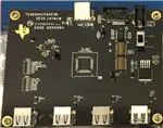
Figure 1. TUSB4041PAPEVM Top Layer Layout
2
TUSB4041PAP Evaluation Module
SLLU227 A – September 2015 – Revised May 2019
Submit Documentation Feedback
Copyright © 2015–2019, Texas Instruments Incorporated
�Hardware Overview
www.ti.com
2
Hardware Overview
The TUSB4041PAPEVM board hardware can be divided into six functional areas:
2.1
TUSB4041PAP
The TUSB4041PAPEVM (U2 on the schematic) operates as a functional interconnect between an
upstream connection to a USB host or hub and up to two directly-connected downstream devices or hubs.
More devices and hubs can be supported if arranged in tiers. The TUSB4041 is capable of supporting
operation at High-Speed (HS), Full Speed (FS), or Low Speed (LS). In general, the speed of the upstream
connection of the TUSB4041PAPEVM limits the downstream connections to that speed (HS and FS) or
lower.
The TUSB4041 requires a 24-MHz low-ESR crystal, Y1 with a 1-MΩ feedback resistor. The crystal should
be fundamental mode with a load capacitance of 12 pF – 24 pF and a frequency stability rating of ±100
PPM or better. To ensure a proper startup oscillation condition, a maximum crystal equivalent series
resistance (ESR) of 50 Ω is recommended.
The TUSB4041 can also use an oscillator or other clock source. When using an external clock source
such as an oscillator, the reference clock should have ±100 PPM (or better) frequency stability and have
less than 50-ps absolute peak-to-peak jitter (or less) than 25-ps peak-to-peak jitter after applying the USB
3.0 jitter transfer function.
2.2
USB Port Connectors
The TUSB4041PAPEVM is equipped with five standard USB2.0 port connectors. One of these five
connectors, J1, is a Type-B connector designed to interface with an upstream USB host or hub. The
remaining connectors, J2, J3, J4, and J5 are Type-A connectors for connection to downstream devices or
hubs. Standard size connectors were used on the EVM design but USB micro connectors can be used, if
desired.
The USB ports can be attached via a standard USB cable to any USB 2.0 host, hub, or device. The
TUSB4041 will automatically connect to any upstream USB 2.0 host or hub at HS.
2.2.1
USB Port Connector - Power
VBUS is received from the upstream host or hub on J1. The TUSB4041 can be configured as a selfpowered or bus-power hub, just setting SW3 in the required option.
When the EVM is set for self-power there is not any significant current draw by the EVM from VBUS. The
TUSB4041 does monitor the VBUS input after filtering through a resistor divider network of a 90.9-kΩ, 1%
resistor, R2, and a 10-kΩ, 1% resistor, R3. VBUS cannot be directly connected to the TUSB4041 device.
A bulk capacitor of at least 1 μF is required on the upstream port VBUS input to comply with the USB
specification. The TUSB4041PAPEVM uses a 10-μF capacitor, C35.
VBUS, sourced by the 5-V wall power input, J6, is provided to the downstream port connectors. The USB
2.0 specification limits the current consumption of a USB 2.0 device to 500 mA at 5 V. The current-limiting
parameter of the TPS2001C device, U7, is configured to 2.2 A to avoid any spurious overcurrent events
due to bus-powered HDD spin-up power fluctuations or unnecessary limiting during USB charging. A
production implementation could place stricter limits on this power consumption. An overcurrent event on
any of the downstream port connectors will be reported to the TUSB4041 via the OVERCURxZ inputs.
2.2.2
USB Port Connector – Noise Filtering
Each downstream VBUS output has a 150-μF bulk capacitor (C70, C71, C76, C79) as recommended by
the TPS2001C data manual (SLVSAU6) to prevent in-rush current events on the downstream devices. In
addition, there are ferrite beads and small capacitors on the VBUS lines to reduce noise and address
ESD/EMI concerns.
The TUSB4041PAPEVM also implements optional isolation using two small noise-filtering capacitors and
a 1-MΩ resistor between the earth ground of each connector and the digital ground of the EVM, this is not
a requirement but should be used if ground isolation is desired.
SLLU227 A – September 2015 – Revised May 2019
Submit Documentation Feedback
Copyright © 2015–2019, Texas Instruments Incorporated
TUSB4041PAP Evaluation Module
3
�Hardware Overview
2.3
www.ti.com
Optional Serial EEPROM
Each TUSB4041PAPEVM is equipped with an onboard EEPROM/socket placeholder, U2. A small I2C
EEPROM can be installed to set the configuration registers as defined in the TUSB4041 data manual
(SLLSEK3A). In its default setting, the EVM does not have an EEPROM installed and instead uses the
configuration inputs to determine any optional settings of the TUSB4041.
The EEPROM interface defaults to programmable (not write-protected) so that any installed EEPROM’s
contents may be modified to test various settings. If an EEPROM data change is required, the values may
be changed using the register access methods outlined in the TUSB4041 data sheet. In addition, a
Microsoft® Windows® based EEPROM utility is available upon request.
2.4
Power
The TUSB4041PAPEVM operates from the power provided by a 5-V wall power adapter, J6, or bus power
supplied by a USB host. It is recommended to use a wall power adapter that is capable of sourcing 4 A to
5 A because the hub must be able to source significant power on its downstream ports (500 mA per port).
The TUSB4041PAPEVM uses a single-channel LDO voltage regulator to drop 5 V to 3.3 V. The
TPS7A4533, U4, is a 1.5-A output linear regulator (SLVS720). The 1.1-V core voltage required by the
TUSB4041 is sourced by the 3.3-V rail to reduce unnecessary heat dissipation. The TPS74801, U6, is a
1.5-A output single-channel LDO linear regulator (SBVS074). Both regulators require few external passive
components and are appropriately rated for heat dissipation.
2.5
Hub Configuration
The TUSB4041PAPEVM can be configured by setting several inputs to the TUSB4041 that are sampled
at power-on reset or using an optional serial EEPROM or SMBUS host. A production implementation
without EEPROM or SMBUS could either rely on the default internal pullup or pulldown resistor for each
configuration input or over-ride it with an external pullup or pulldown resistor. The settings can be modified
using SW1 and SW2 on the EVM. Descriptions of the possible configuration changes are included in
Section 3.1.
2.6
Optional Circuitry
The following list provides the optional circuitry available on the TUSB4041PAPEVM:
• D4 – Indicates BOARD_3P3V is active
• The switch (SW1, SW2) and headers (J8, JP6) provided on the TUSB4041PAPEVM are intended for
lab evaluation only and are not required for production designs.
4
TUSB4041PAP Evaluation Module
SLLU227 A – September 2015 – Revised May 2019
Submit Documentation Feedback
Copyright © 2015–2019, Texas Instruments Incorporated
�Hardware Set Up
www.ti.com
3
Hardware Set Up
3.1
Configuration Switch
The TI TUSB4041PAPEVM has a set of switches to facilitate configuration changes. Changing these
switch settings without a complete understanding of the result is not recommended. Configuration inputs
are only read by the TUSB4041 during power on reset, changing the switch settings while the EVM is
powered on will have no effect. Please refer to the EVM schematics for additional information (included in
the appendix).
The switch definitions are as follows, with the standard setting in parenthesis:
SW1_1 (off):
SW1_2 (off):
SW1_3 (off):
SW1_4 (off):
SW1_5 (off):
SW1_6(off):
SW1_7 (off):
SW1_8(off):
SW2_1 (on):
SW2_2 (on):
TEST_TRSTZ. This pin is reserved for factory test.
SMBUSz Switch. The TUSB4041 has an internal pullup on this terminal, so I2C interface
mode is enabled by default. If the switch is set to the ON position, the terminal is pulled
low and SMBUS mode is enabled.
SCL_SMBCLK Switch. The TUSB4041 has an internal pulldown on this terminal, so the
serial EEPROM/SMBUS interface is disabled. If the switch is set to the ON position, a
pullup resistor is connected to the serial clock terminal to indicate that an I2C EEPROM
may be attached (along with a pullup resistor on SDA).
SDA_SMBDAT Switch. The TUSB4041 has an internal pulldown on this terminal, so the
serial EEPROM/SMBUS interface is disabled. If the switch is set to the ON position, a
pullup resistor is connected to the serial clock terminal to indicate that an I2C EEPROM
may be attached (along with a pullup resistor on SCL).
PWRCTL1_BATEN1 Switch. The TUSB4041 has an internal pulldown on this terminal,
so USB Battery Charging mode on Port 1 is disabled by default. If the switch is set to the
ON position, the terminal is pulled high and battery charging is enabled on downstream
Port 1.
PWRCTL2_BATEN2 Switch. The TUSB4041 has an internal pulldown on this terminal,
so USB Battery Charging mode on Port 2 is disabled by default. If the switch is set to the
ON position, the terminal is pulled high and battery charging is enabled on downstream
Port 2.
PWRCTL1_BATEN1 Switch. The TUSB4041 has an internal pulldown on this terminal,
so USB Battery Charging mode on Port 3 is disabled by default. If the switch is set to the
ON position, the terminal is pulled high and battery charging is enabled on downstream
Port 3.
PWRCTL2_BATEN2 Switch. The TUSB4041 has an internal pulldown on this terminal,
so USB Battery Charging mode on Port 4 is disabled by default. If the switch is set to the
ON position, the terminal is pulled high and battery charging is enabled on downstream
Port 4.
AUTOENZ Switch. Automatic charge mode enable/HS suspend status The value of the
pin is sampled at the deassertion of reset to determine if automatic mode is enabled as
follows:
0 = Automatic mode is enabled on ports that are enabled for battery charging when the
hub is unconnected. Note that CDP is not supported on Port 1 when operating in
automatic mode.
1 = Automatic mode is disabled.
This value is also used to set the autoEnz bit in the Battery Charging Support Register.
After reset, this signal indicates the high-speed USB suspend status of the upstream port
if enabled through the Additional Feature Configuration Register. When enabled, a value
of 1 indicates the connection is suspended.
GANGED_HS_UP Switch. The TUSB4041 has an internal pulldown on this terminal, so
individual port power control mode is enabled by default. If the switch is set to the ON
position, the terminal is pulled high and ganged mode is enabled. Since the
TUSB4041PAPEVM does implement individual port power controls, this terminal should
be set low.
SLLU227 A – September 2015 – Revised May 2019
Submit Documentation Feedback
Copyright © 2015–2019, Texas Instruments Incorporated
TUSB4041PAP Evaluation Module
5
�EVM Installation
SW2_3 (off):
SW2_4 (on):
SW2_5 (off):
SW2_6 (off):
SW2_7 (NC):
SW2_8 (NC):
4
www.ti.com
PWRCTL_POL_TDO Switch. The TUSB4041 has an internal pulldown on this terminal,
so port power control polarity defaults to active high. If the switch is set to the ON
position, the terminal is pulled high and the port power control polarity changes to active
low.
FULLPWRMGMTZ. The TUSB4041 has an internal pulldown on this terminal, so the
TUSB4041 defaults to a full power management mode. If the switch is set to the ON
position, the terminal is pulled high and full power management mode is disabled. In full
power management mode, the TUSB4041 reports that it supports downstream port
power switching in the USB descriptors it sends to the USB host. Since the
TUSB4041PAPEVM implements downstream port power switching, full power
management mode should be enabled.
SCL_SMBCLK Switch. The TUSB4041 has an internal pulldown on this terminal, so the
serial EEPROM/SMBUS interface is disabled. If the switch is set to the ON position, a
pullup resistor is connected to the serial clock terminal to indicate that an I2C EEPROM
may be attached (along with a pullup resistor on SDA).
SDA_SMBDAT Switch. The TUSB4041 has an internal pulldown on this terminal, so the
serial EEPROM/SMBUS interface is disabled. If the switch is set to the ON position, a
pullup resistor is connected to the serial clock terminal to indicate that an I2C EEPROM
may be attached (along with a pullup resistor on SCL).
Not connected
Not connected
EVM Installation
To install the EVM, perform the following steps:
1. Attach a 5-V, 3-A wall power source to J6. LEDs D4 should be lit.
2. Attach a USB cable between J4 and a USB host. LEDs D1, should be lit.
5
Troubleshooting
Case 1: Device function(s) are “banged out” in Device Manager.
• Make sure that the latest updates are installed for the operating system
• Make sure that the latest drivers are installed for the host controller
Case 2: The EVM does not work at all.
• Verify that all switches are in their default state and the EVM is powered on with a 5-V source with
adequate current to support any bus-powered devices (3 A+).
• If installed, remove the serial EEPROM from the EEPROM socket. The EVM does not require an
EEPROM to operate.
• In the case where a 12-V power supply has been attached to the EVM, the fault is non-recoverable.
6
TUSB4041PAP Evaluation Module
SLLU227 A – September 2015 – Revised May 2019
Submit Documentation Feedback
Copyright © 2015–2019, Texas Instruments Incorporated
�Appendix A
SLLU227 A – September 2015 – Revised May 2019
A.1
TUSB4041PAPEVM Bill of Materials
This appendix contains the TUSB4041PAPEVM BOM.
Table 1. TUSB4041PAPEVM BOM
Item
Part
Manufacturer
Part Number
1
Qty Reference
2
C1,C2
18pF
AVX
04025A180JAT2A
2
1
C3
1uF
Samsung
CL05B105KQ5NQNC
3
18
C4,C38,C40,C41,C46,C48,C50,C51,C56,C 0.1uF
58,C66,C69,C72,C75,C77,C78,C80,C81
Yageo
CC0402KRX5R6BB104
4
1
C5
TDK
CL21B105KPFNNNE
5
11
C6,C9,C12,C15,C19,C22,C25,C28,C32,C8 0.001uF
3,C86
TDK
C0603X7R1E102K030BA
6
11
C7,C10,C13,C16,C20,C23,C26,C29,C33,C 0.01uF
85,C88
Yageo
CC0201KRX7R7BB103
7
11
C8,C11,C14,C17,C21,C24,C27,C30,C34,C 0.1uF
84,C87
TDK
C0603X5R0J104M
8
8
C18,C31,C35,C67,C68,C73,C74,C82
10uF
Murata Electronics
GRM31CR71C106KAC7L
1uF
9
5
C39,C47,C49,C57,C59
0.001uF
TDK
C1005X7R1H102K
10
4
C70,C71,C76,C79
150uF
Kemet
T495D157K010ATE100
11
2
D1,D4
LED Green 0805
Lite On
LTST-C171GKT
12
6
FB1,FB2,FB3,FB4,FB5,FB6
220 @ 100MHZ
Murata
BLM18PG221SN1D
13
2
GND1,GND2
TEST POINT
Wurth Electronics Inc
61300111121
14
1
JP6
Conn 2x5 shroud
3M
N2510-6002-RB
15
1
J1
Type B USB-Shield
FCI
61729-1011BLF
16
4
J2,J3,J4,J5
Type A USB-Shield
TE Connectivity AMP
Connectors
292303-1
17
1
J6
2.1mm x 5.5mm
CUI Inc.
PJ-202AH (PJ-002AH)
18
3
J7,J8,J9
Header 1x2
3M
961102-6404-AR
19
6
R1,R15,R17,R18,R19,R20
1M
Rohm Semiconductor
MCR01MZPJ105
20
1
R2
90.9K
Rohm Semiconductor
RMCF0402FT90K9
21
5
R3,R26,R27,R29,R36
10K
Rohm Semiconductor
MCR01MZPF1002
22
14
R4,R5,R11,R12,R13,R14,R22,R23,R24,R2 1K
5,R38,R39,R46,R47
Rohm Semiconductor
MCR01MRTJ102
23
4
R6,R7,R8,R9
4.7K
Rohm Semiconductor
MCR01MZPJ472
24
0
R10,R32,R42,R43,R44,R45
10K NOPOP
Rohm Semiconductor
MCR01MZPF1002
25
2
R16,R28
330
Rohm Semiconductor
MCR01MZPJ331
26
1
R21
9.53K
Rohm Semiconductor
MCR01MRTF9531
27
1
R33
1.87K
Vishay / Dale
CRCW04021K87FKED
28
1
R34
4.99K
Vishay / Dale
CRCW04024K99FKED
29
2
SW1,SW2
8-POS 50-MIL SMT
C&K Components
TDA08H0SB1R
30
1
SW3
MS13ANW03
NKK Switches
MS13ANW03
31
1
U1
TUSB4041
Texas Instruments
TUSB4041IPAP
32
1
U2
24AA04-I/P
Microchip Technology
24AA04-I/P
33
1
U4
TPS7A4533
Texas Instruments
TPS7A4533KTT
34
1
U6
TPS74801RGW
Texas Instruments
TPS74801RGW
35
4
U7,U8,U9,U10
TPS2001C
Texas Instruments
TPS2001CDGN
36
1
Y1
ECS-24MHZ
ECS
ECS-240-20-30B-TR
SLLU227 A – September 2015 – Revised May 2019
Submit Documentation Feedback
Copyright © 2015–2019, Texas Instruments Incorporated
7
�TUSB4041PAPEVM Schematics
A.2
www.ti.com
TUSB4041PAPEVM Schematics
Figure 2 through Figure 4 illustrate the TUSB4041PAPEVM schematics.
R1
1M
Y1
VDD33
USB_DM_UP
USB_DP_UP
VDD11
ECS-24MHZ
18pF
TEST_TRSTZ
2
2
C3
9.53K
1%
33
34
35
36
37
38
39
40
41
42
43
44
45
46
47
48
USB_DP_DN1
USB_DM_DN1
USB_DP_DN2
USB_DM_DN2
R3
10K
0402
1%
1uF
32
31
30
29
28
27
26
25
24
23
22
21
20
19
18
17
USB_DP_DN1
USB_DM_DN1
RSVD5
RSVD6
VDD
RSVD7
RSVD8
NC2
USB_DP_DN2
USB_DM_DN2
RSVD9
RSVD10
VDD
RSVD11
RSVD12
VDD33
USB_VBUS
OVERCUR2z
OVERCUR1z
AUTOENz/HS_SUSPEND
OVERCUR3z
OVERCUR4z
GANGED/SMBA2/HS_UP
PWRCTL_POL
FULLPWRMGMTz/SMBA1
SMBUSz
SCL/SMBCLK
SDA/SMBDAT
PWRCTL1/BATEN1
PWRCTL2/BATEN2
VDD33
PWRCTL3/BATEN3
BOARD_3P3V
USB_VBUS_UP
2
Header 1x2
90.9K
0402
1%
16
15
14
13
12
11
10
9
8
7
6
5
4
3
2
1
2
R45
10K NOPOP
OVERCUR2Z_TMS
OVERCUR1Z_TDI
AUTOENZ
GANGED_HS_UP
PWRCTL_POL_TDO
FULLPWRMGMTZ
SMBUSZ
SCL_SMBCLK
SDA_SMBDAT
OVERCUR2Z_TMS
OVERCUR1Z_TDI
3
3
OVERCUR3Z_TCK
OVERCUR4Z
3
3
R44
R43
R42
10K NOPOP 10K NOPOP 10K NOPOP
JP6
TEST_TRSTZ
PWRCTL_POL_TDO
OVERCUR1Z_TDI
OVERCUR2Z_TMS
OVERCUR3z_TCK
1
3
5
7
9
JTAG is for lab evaluation only on TUSB8041.
This header and NOPOP pullups are not recommended
for customers.
PWRON1_BATEN1
PWRON2_BATEN2
PWRON3_BATEN3
PWRON4_BATEN4
65
PPAD
TEST_TRSTZ
SMBUSZ
SCL_SMBCLK
SDA_SMBDAT
PWRON1_BATEN1
PWRON2_BATEN2
PWRON3_BATEN3
PWRON4_BATEN4
USB_DP_DN3
USB_DM_DN3
2
2
Conn 2x5 shroud
BOARD_3P3V
R22
1K
0402
5%
SW1
8-POS 50-MIL SMT
2
2
2
4
6
8
10
3
3
3
3
49
50
51
52
53
54
55
56
57
58
59
60
61
62
63
64
TUSB4041
USB_R1
VDD33
XI
XO
NC1
RSVD4
RSVD3
VDD
RSVD2
RSVD1
USB_DM_UP
USB_DP_UP
VDD33
VDD
GRSTz
TEST
C2
18pF
2
2
J8
1
USB_DP_DN3
USB_DM_DN3
RSVD13
RSVD14
VDD
RSVD15
RSVD16
USB_DP_DN4
USB_DM_DN4
RSVD17
RSVD18
VDD
RSVD19
RSVD20
VDD
PWRCTL4/BATEN4
C1
R21
U1
2
2
R2
GRSTZ
1
2
3
4
5
6
7
8
R4
1K
0402
5%
R5
1K
0402
5%
R6
4.7K
0402
5%
R7
4.7K
0402
5%
R8
4.7K
0402
5%
R9
4.7K
0402
5%
TEST_PUP
SMBUSZ_PD
SCL_PUP
SDA_PUP
BATEN0
BATEN1
BATEN2
BATEN3
16
15
14
13
12
11
10
9
USB_DP_DN4
USB_DM_DN4
R24
1K
0402
5%
BOARD_3P3V
BOARD_3P3V
C4
0.1uF
Optional EEPROM Circuitry
R10
10K NOPOP
R23
1K
0402
5%
U2
1
2
3
4
R11
1K
0402
5%
R12
1K
0402
5%
A0
A1
A2
GND
R13
1K
0402
5%
VCC
WP
SCLK
SDATA
8
7
6
5
SW2
8-POS 50-MIL SMT
SCL_SMBCLK
SDA_SMBDAT
1
2
3
4
5
6
7
8
AUTOENZ
GANGED_HS_UP
PWRCTL_POL_TDO
FULLPWRMGMTZ
AT24C04
R14
1K
0402
5%
VDD33
16
15
14
13
12
11
10
9
R25
1K
0402
5%
R38
1K
0402
5%
AUTOENZ_PD
GANGED_PU
PWRCTL_POL_PD
FULLPWRMGMTZ_PUP
SCL_PD
SDA_PD
R46
1K
0402
5%
R47
1K
0402
5%
R39
1K
0402
5%
BOARD_3P3V
C5
1uF
C6
0.001uF
C7
0.01uF
C8
C9
C10
0.1uF
0.001uF
0.01uF
C11
0.1uF
C12
C13
C14
C15
C16
C17
0.001uF
0.01uF
0.1uF
0.001uF
0.01uF
0.1uF
220 @ 100MHZ
GND1
J7
2
GND2
1
1
1
FB1
Header 1x2
VDD11
BOARD_1P1V
FB2
J9
1
C18
10uF
C19
C20
C21
C22
C23
C24
C25
C26
C27
C28
C29
C30
0.001uF
0.01uF
0.1uF
0.001uF
0.01uF
0.1uF
0.001uF
0.01uF
0.1uF
0.001uF
0.01uF
0.1uF
C31
10uF
C32
C33
C34
C83
C85
C84
C86
C88
C87
0.001uF
0.01uF
0.1uF
0.001uF
0.01uF
0.1uF
0.001uF
0.01uF
0.1uF
220 @ 100MHZ
2
Header 1x2
Figure 2. TUSB4041PAPEVM Schematics
8
SLLU227 A – September 2015 – Revised May 2019
Submit Documentation Feedback
Copyright © 2015–2019, Texas Instruments Incorporated
�TUSB4041PAPEVM Schematics
www.ti.com
Type B USB-Shield
+5V 1
7
USB_VBUS_UP
DM 2
DP 3
USB_DM_UP
1
USB_DP_UP
1
C35
10uF
GND 4
8
1
D1
LED Green 0805
J1
C38
0.1uF
R16
330
0402
5%
R15
1M
0402
5%
C39
0.001uF
FB3
J2
VBUS_DS4
DN4_VBUS
8
C40
0.1uF
+5V 1
FB4
DN4_VBUS
3
J3
VBUS_DS2
220 @ 100MHZ
DP 3
USB_DM_DN4
1
USB_DP_DN4
1
DP 3
GND 4
7
7
USB_DM_DN2
1
USB_DP_DN2
1
Type A USB-Shield
C46
0.1uF
C47
0.001uF
R17
1M
0402
5%
C48
0.1uF
C49
0.001uF
FB5
VBUS_DS1
J4
3
DM 2
GND 4
Type A USB-Shield
DN2_VBUS
C41 220 @ 100MHZ
0.1uF
+5V 1
DM 2
DN2_VBUS
8
8
DN1_VBUS
C50
0.1uF
R18
1M
0402
5%
FB6
DN1_VBUS
3
220 @ 100MHZ
VBUS_DS3
J5
8
+5V 1
DN3_VBUS
C51
0.1uF
DN3_VBUS
3
220 @ 100MHZ
+5V 1
DM 2
DP 3
GND 4
USB_DM_DN1
1
DM 2
USB_DP_DN1
1
DP 3
USB_DM_DN3
1
USB_DP_DN3
1
GND 4
7
7
Type A USB-Shield
Type A USB-Shield
C56
0.1uF
C57
0.001uF
R19
1M
0402
5%
C58
0.1uF
C59
0.001uF
R20
1M
0402
5%
Figure 3. TUSB4041PAPEVM USB2 Connector Schematics
9
SLLU227 A – September 2015 – Revised May 2019
Submit Documentation Feedback
Copyright © 2015–2019, Texas Instruments Incorporated
�TUSB4041PAPEVM Schematics
www.ti.com
5V INPUT
DOWNSTREAM PORT POWER SWITCHES
BOARD_3P3V
BOARD_5V
SILKSCREEN: TIP +5v
BOARD_5V
J6
2
3
1
SW3
MS13ANW03
3 1
2
R26
10K
0402
5%
C66
S
T
2.1mm x 5.5mm
0.1uF
U7
USB_VBUS_UP
C82
10uF
1
2
3
4
PWRON1_BATEN1
1
PWRON1_BATEN1
GND
IN
IN
EN
OUT
OUT
OUT
FLT
PAD
8
7
6
5
DN1_VBUS
DN1_VBUS
2
OVERCUR1Z_TDI
1
9
C69
TPS2001C
C70
150uF
+
0.1uF
BOARD_3P3V
BOARD_5V
R27
10K
0402
5%
C75
0.1uF
U8
BOARD_5V
3.3V REGULATOR
1
2
3
4
PWRON2_BATEN2
1
BOARD_3P3V
PWRON2_BATEN2
GND
IN
IN
EN
OUT
OUT
OUT
FLT
PAD
DN2_VBUS
OVERCUR2Z_TMS
C72
5
C68
10uF
GND
SENSE
1
4
D4
LED Green 0805
BOARD_3P3V
BOARD_5V
6
SHDN/
TPS7A4533
GND
OUT
2
C71
150uF
+
0.1uF
IN
3
1
C67
10uF
DN2_VBUS
9
TPS2001C
U4
2
8
7
6
5
R28
330
0402
5%
R29
10K
0402
5%
C78
0.1uF
U9
1
2
3
4
PWRON3_BATEN3
1
PWRON3_BATEN3
GND
IN
IN
EN
OUT
OUT
OUT
FLT
PAD
8
7
6
5
DN3_VBUS
DN3_VBUS
2
OVERCUR3Z_TCK
1
9
C77
TPS2001C
+
0.1uF
C76
150uF
1.1V REGULATOR
1P1V_SS
BOARD_3P3V
BOARD_1P1V
R32
10K NOPOP
2
3
4
13
14
17
15
TPS74801RGW
GND
GND
BIAS
OUT1
OUT2
OUT3
OUT4
FB
21
10
IN1
IN2
IN3
IN4
EN
12
C73
10uF
NC1
NC2
NC3
NC4
NC5
NC6
SS
U6
5
6
7
8
11
BOARD_3P3V
BOARD_5V
PG
9
R36
10K
0402
5%
C81
1
18
19
20
16
0.1uF
1P1V_FB
R33
1.87K
0402
5%
U10
C74
10uF
PWRON4_BATEN4
1
PWRON4_BATEN4
1
2
3
4
R34
4.99K
0402
5%
GND
IN
IN
EN
OUT
OUT
OUT
FLT
PAD
TPS2001C
8
7
6
5
DN4_VBUS
DN4_VBUS
OVERCUR4Z
2
1
9
C80
0.1uF
+
C79
150uF
Figure 4. TUSB4041PAPEVM Power Schematics
10
SLLU227 A – September 2015 – Revised May 2019
Submit Documentation Feedback
Copyright © 2015–2019, Texas Instruments Incorporated
�Revision History
www.ti.com
Revision History
NOTE: Page numbers for previous revisions may differ from page numbers in the current version.
Changes from Original (September 2015) to A Revision ............................................................................................... Page
•
Changed SW2_2 and SW2_4 descriptions ............................................................................................ 5
SLLU227 A – September 2015 – Revised May 2019
Submit Documentation Feedback
Copyright © 2015–2019, Texas Instruments Incorporated
Revision History
11
�IMPORTANT NOTICE AND DISCLAIMER
TI PROVIDES TECHNICAL AND RELIABILITY DATA (INCLUDING DATA SHEETS), DESIGN RESOURCES (INCLUDING REFERENCE
DESIGNS), APPLICATION OR OTHER DESIGN ADVICE, WEB TOOLS, SAFETY INFORMATION, AND OTHER RESOURCES “AS IS”
AND WITH ALL FAULTS, AND DISCLAIMS ALL WARRANTIES, EXPRESS AND IMPLIED, INCLUDING WITHOUT LIMITATION ANY
IMPLIED WARRANTIES OF MERCHANTABILITY, FITNESS FOR A PARTICULAR PURPOSE OR NON-INFRINGEMENT OF THIRD
PARTY INTELLECTUAL PROPERTY RIGHTS.
These resources are intended for skilled developers designing with TI products. You are solely responsible for (1) selecting the appropriate
TI products for your application, (2) designing, validating and testing your application, and (3) ensuring your application meets applicable
standards, and any other safety, security, regulatory or other requirements.
These resources are subject to change without notice. TI grants you permission to use these resources only for development of an
application that uses the TI products described in the resource. Other reproduction and display of these resources is prohibited. No license
is granted to any other TI intellectual property right or to any third party intellectual property right. TI disclaims responsibility for, and you
will fully indemnify TI and its representatives against, any claims, damages, costs, losses, and liabilities arising out of your use of these
resources.
TI’s products are provided subject to TI’s Terms of Sale or other applicable terms available either on ti.com or provided in conjunction with
such TI products. TI’s provision of these resources does not expand or otherwise alter TI’s applicable warranties or warranty disclaimers for
TI products.
TI objects to and rejects any additional or different terms you may have proposed. IMPORTANT NOTICE
Mailing Address: Texas Instruments, Post Office Box 655303, Dallas, Texas 75265
Copyright © 2022, Texas Instruments Incorporated
�


 工商网监
湘ICP备2023018690号
工商网监
湘ICP备2023018690号
