TUSB8040
USB 3.0 Four Port Hub
Data Manual
PRODUCTION DATA information is current as of publication date.
Products conform to specifications per the terms of the Texas
Instruments standard warranty. Production processing does not
necessarily include testing of all parameters.
Literature Number: SLLSE42I
September 2010 – Revised September 2013
�Not Recommended for New Designs
TUSB8040
www.ti.com
SLLSE42I – SEPTEMBER 2010 – REVISED SEPTEMBER 2013
Contents
1
PRODUCT OVERVIEW
1.1
1.2
1.3
2
3
4
5
6
2
......................................................................................................... 5
Features ...................................................................................................................... 5
Introduction .................................................................................................................. 6
Functional Block Diagram .................................................................................................. 7
............................................................................................................. 8
2.1
Clock and Reset Signals ................................................................................................... 9
2.2
USB Upstream Signals ..................................................................................................... 9
2.3
USB Downstream Signals ................................................................................................ 10
2.4
I2C/SMBUS Signals ....................................................................................................... 11
2.5
Test and Miscellaneous Signals ......................................................................................... 11
2.6
Power Signals .............................................................................................................. 12
FUNCTIONAL DESCRIPTION ............................................................................................... 13
3.1
I2C EEPROM Operation .................................................................................................. 13
3.2
SMBus Slave Operation .................................................................................................. 13
3.3
Configuration Registers ................................................................................................... 14
3.3.1
ROM Signature Register ....................................................................................... 14
3.3.2
Vendor ID LSB Register ....................................................................................... 14
3.3.3
Vendor ID MSB Register ...................................................................................... 14
3.3.4
Product ID LSB Register ....................................................................................... 15
3.3.5
Product ID MSB Register ...................................................................................... 15
3.3.6
Device Configuration Register ................................................................................ 15
3.3.7
Battery Charging Support Register ........................................................................... 16
3.3.8
Device Removable Configuration Register .................................................................. 17
3.3.9
Port Used Configuration Register ............................................................................ 17
3.3.10 Language ID LSB Register .................................................................................... 18
3.3.11 Language ID MSB Register ................................................................................... 18
3.3.12 Serial Number String Length Register ....................................................................... 18
3.3.13 Manufacturer String Length Register ........................................................................ 19
3.3.14 Product String Length Register ............................................................................... 19
3.3.15 Serial Number Registers ....................................................................................... 19
3.3.16 Manufacturer String Registers ................................................................................ 20
3.3.17 Product String Registers ....................................................................................... 20
3.3.18 Device Status and Command Register ...................................................................... 20
CLOCK GENERATION ........................................................................................................ 21
4.1
Crystal Requirements ..................................................................................................... 21
4.2
Input Clock Requirements ................................................................................................ 21
POWER UP AND RESET ..................................................................................................... 22
ELECTRICAL SPECIFICATIONS .......................................................................................... 23
6.1
ABSOLUTE MAXIMUM RATINGS ...................................................................................... 23
6.2
RECOMMENDED OPERATING CONDITIONS ....................................................................... 23
6.3
THERMAL INFORMATION .............................................................................................. 24
6.4
3.3-V I/O ELECTRICAL CHARACTERISTICS ........................................................................ 25
6.5
HUB INPUT SUPPLY CURRENT ....................................................................................... 26
PIN DESCRIPTIONS
Contents
Copyright © 2010–2013, Texas Instruments Incorporated
�Not Recommended for New Designs
TUSB8040
www.ti.com
SLLSE42I – SEPTEMBER 2010 – REVISED SEPTEMBER 2013
List of Figures
1-1
Typical Application .................................................................................................................
6
1-2
TUSB8040PFP Functional Block Diagram .....................................................................................
7
4-1
TUSB8040 Clock .................................................................................................................
21
Copyright © 2010–2013, Texas Instruments Incorporated
List of Figures
3
�Not Recommended for New Designs
TUSB8040
SLLSE42I – SEPTEMBER 2010 – REVISED SEPTEMBER 2013
www.ti.com
List of Tables
2-1
Clock and Reset Signals ..........................................................................................................
9
2-2
USB Upstream Signals............................................................................................................
9
2-3
USB Downstream Signals .......................................................................................................
10
2-4
I2C/SMBUS Signals ..............................................................................................................
11
2-5
Test and Miscellaneous Signals ................................................................................................
11
2-6
Power Signals
....................................................................................................................
TUSB8040 Register Map ........................................................................................................
Register Offset 0h ................................................................................................................
Bit Descriptions – ROM Signature Register ..................................................................................
Register Offset 1h ................................................................................................................
Bit Descriptions – Vendor ID LSB Register ..................................................................................
Register Offset 2h ................................................................................................................
Bit Descriptions – Vendor ID MSB Register .................................................................................
Register Offset 3h ................................................................................................................
Bit Descriptions – Product ID MSB Register .................................................................................
Register Offset 4h ................................................................................................................
Bit Descriptions – Product ID MSB Register .................................................................................
Register Offset 5h ................................................................................................................
Bit Descriptions – Device Configuration Register ...........................................................................
Register Offset 6h ................................................................................................................
Bit Descriptions – Battery Charging Support Register ......................................................................
Register Offset 7h ................................................................................................................
Bit Descriptions – Device Removable Configuration Register .............................................................
Register Offset 8h ................................................................................................................
Bit Descriptions – Port Used Configuration Register .......................................................................
Register Offset 20h ..............................................................................................................
Bit Descriptions – Language ID LSB Register ...............................................................................
Register Offset 21h ..............................................................................................................
Bit Descriptions – Language ID LSB Register ...............................................................................
Register Offset 22h ..............................................................................................................
Bit Descriptions – Serial Number String Length Register ..................................................................
Register Offset 23h ..............................................................................................................
Bit Descriptions – Manufacturer String Length Register ...................................................................
Register Offset 24h ..............................................................................................................
Bit Descriptions – Product String Length Register ..........................................................................
Register Offset 30h-4Fh .........................................................................................................
Bit Descriptions – Serial Number Byte N Register ..........................................................................
Register Offset 50h-8Fh .........................................................................................................
Bit Descriptions – Manufacturer String Register ............................................................................
Register Offset 90h-CFh ........................................................................................................
Bit Descriptions – Product String Register ...................................................................................
Register Offset F8h ..............................................................................................................
Bit Descriptions – Device Status and Command Register .................................................................
12
3-1
3-2
3-3
3-4
3-5
3-6
3-7
3-8
3-9
3-10
3-11
3-12
3-13
3-14
3-15
3-16
3-17
3-18
3-19
3-20
3-21
3-22
3-23
3-24
3-25
3-26
3-27
3-28
3-29
3-30
3-31
3-32
3-33
3-34
3-35
3-36
3-37
4
List of Tables
13
14
14
14
14
14
14
15
15
15
15
15
15
16
16
17
17
17
17
18
18
18
18
18
18
19
19
19
19
19
19
20
20
20
20
20
20
Copyright © 2010–2013, Texas Instruments Incorporated
�Not Recommended for New Designs
TUSB8040
www.ti.com
SLLSE42I – SEPTEMBER 2010 – REVISED SEPTEMBER 2013
USB 3.0 Four Port Hub
Check for Samples: TUSB8040
1
PRODUCT OVERVIEW
1.1
Features
• USB 3.0 Compliant Four Port Hub, TID# 330000003
– Upstream Port Supports SuperSpeed, High-Speed and Full-Speed Connections
– Each of the Four Downstream Ports Support SuperSpeed, High-Speed, Full-Speed/Low-Speed
Connections
• USB 2.0 Hub Features
– Multi Transaction Translator (MTT) Hub: Four Transaction Translators, One Per Port
– Four (Over USB Required Minimum of Two) Asynchronous Endpoint Buffers Per Transaction
Translator for Better Throughput
• Supports Charging Downstream Port (CDP) Applications
– Battery Charging 1.2 Compliant
• Supports Operation as a USB 3.0 or USB 2.0 Compound Device
• Supports Per Port or Ganged Power Switching and Over-Current Protection
• Provides the following status outputs:
– High-Speed Upstream Connection
– High-Speed Upstream Port Suspended
– SuperSpeed Upstream Connection
– SuperSpeed Upstream Port Suspended
• Optional Serial EEPROM or SMBus Slave Interface for Custom Configurations:
– VID/PID
– Manufacturer and Product Strings
– Serial Number
• Using Pin Selection or the EEPROM/SMBus Slave Interface, Each Downstream Port Can Be
Independently:
– Enabled or Disabled
– Marked as Removable or Permanently Attached (for Compound Applications)
– Have Battery Charging Enabled or Disabled
• Provides 128-Bit Universally Unique Identifier (UUID)
• Optionally Supports USB 2.0 Compliant Port Indicator LEDs
• Configurable SMBus Address to Support Multiple Devices on the Same SMBus Segment
• Supports On-Board and In-System EEPROM Programming Via the USB 2.0 Upstream Port
• Single Clock Input, 24-MHz Crystal or Oscillator
• No Special Driver Requirements; Works Seamlessly With Any Operating System With USB Stack
Support
1
1
Please be aware that an important notice concerning availability, standard warranty, and use in critical applications of
Texas Instruments semiconductor products and disclaimers thereto appears at the end of this data sheet.
PRODUCTION DATA information is current as of publication date. Products conform to
specifications per the terms of the Texas Instruments standard warranty. Production
processing does not necessarily include testing of all parameters.
Copyright © 2010–2013, Texas Instruments Incorporated
�Not Recommended for New Designs
TUSB8040
SLLSE42I – SEPTEMBER 2010 – REVISED SEPTEMBER 2013
1.2
www.ti.com
Introduction
The TUSB8040 is USB 3.0 compliant hub available in an 80-pin QFP package. The device is designed for
operation over the commercial temperature range of 0°C to 70°C.
The TUSB8040 provides simultaneous SuperSpeed and high-speed/full-speed connections on the
upstream port and provides SuperSpeed, high-speed, full-speed, or low-speed connections on the
downstream ports. When the upstream port is connected to an electrical environment that only supports
high-speed or full-speed/low-speed connections, SuperSpeed connectivity is disabled on the downstream
ports. When the upstream port is connected to an electrical environment that only supports full-speed/lowspeed connections, SuperSpeed and high-speed connectivity are disabled on the downstream ports.
The TUSB8040 supports up to four downstream ports. It may be configured to report one to four
downstream ports by pin selection or an attached EEPROM or SMBus controller. The configuration
options provide the ability to scale the device by application.
A typical system view of the TUSB8040 is shown in Figure 1-1.
USB 3.0 System Implementation
USB 3.0 Host Controller
USB 3.0
Device
TUSB8040
USB 2.0
Device
USB 3.0
Hub
USB 1.1
Device
USB 2.0
Device
USB 2.0 Hub
USB 3.0
Device
USB 2.0
Device
USB 3.0
Device
USB 1.1
Device
USB 1.x Connection
USB 2.0 Connection
USB 2.0/3.0 Device
USB 2.0 Device
USB 3.0 Connection
USB 3.0 Device
USB 1.x Device
Figure 1-1. Typical Application
6
PRODUCT OVERVIEW
Copyright © 2010–2013, Texas Instruments Incorporated
Submit Documentation Feedback
Product Folder Links: TUSB8040
�Not Recommended for New Designs
TUSB8040
www.ti.com
1.3
SLLSE42I – SEPTEMBER 2010 – REVISED SEPTEMBER 2013
Functional Block Diagram
The TUSB8040PFP (QFP) is a reduced footprint hub that supports ganged power switching and overcurrent protection only. A ganged hub switches on power to all its downstream ports when power is
required to be on for any port. The power to the downstream ports is not switched off unless all ports are
in a state that allows power to be removed. Also when a ganged hub senses an over-current event, power
to all downstream ports will be switched off. The TUSB8040PFP also provides customization using an I2C
EEPROM or configuration via an SMBus host for vendor specific PID, VID, and strings. Ports can also be
marked as disabled or permanently attached using an I2C EEPROM or an SMBus host.
The Device Status and Command Register at F8h cannot be modified by the contents of the I2C
EEPROM.
USB_SSTXM_UP
USB_SSTXP_UP
USB_SSRXM_UP
USB_SSRXP_UP
USB_VBUS
VSS
USB_DM_UP
USB_DP_UP
USB_R1
VDD11
USB_R1RTN
VDD33
Power
Distribution
VBUS
Detect
USB 2.0 Hub
SuperSpeed Hub
USB_SSTXM_DN3
USB_SSTXP_DN3
USB_SSRXM_DN3
USB_SSRXP_DN3
USB_SSTXM_DN2
USB_SSTXP_DN2
USB_SSRXM_DN2
USB_SSRXP_DN2
USB_SSTXM_DN1
USB_SSTXP_DN1
USB_SSRXM_DN1
USB_SSRXP_DN1
USB_SSTXM_DN0
USB_SSTXP_DN0
USB_SSRXM_DN0
USB_SSRXP_DN0
USB_DM_DN3
USB_DP_DN3
Clock
and
Reset
Distribution
USB_DM_DN2
USB_DP_DN2
GRSTz
USB_DM_DN1
USB_DP_DN1
Oscilator
USB_DM_DN0
USB_DP_DN0
XI
VSSOSC
XO
SS
SS_SUSPEND
HS
HS_SUSPEND
FULLPWRMGMTz_SMBA1
GPIO
Block
Control
Registers
I2C/
SMBUS
SCL/SMBCLK
SDA/SMDAT
SMBUSz
PWRON0z_BATEN0
OVERCUR0z
Boundary
Scan
JTAG_TRSTn
JTAG_TDI
JTAG_TDO
JTAG_TMS
JTAG_TCK
Figure 1-2. TUSB8040PFP Functional Block Diagram
PIN DESCRIPTIONS
Copyright © 2010–2013, Texas Instruments Incorporated
Submit Documentation Feedback
Product Folder Links: TUSB8040
7
�Not Recommended for New Designs
TUSB8040
SLLSE42I – SEPTEMBER 2010 – REVISED SEPTEMBER 2013
2
www.ti.com
PIN DESCRIPTIONS
60
59
58
57
56
55
54
53
52
51
50
49
48
47
46
45
44
43
42
41
USB_DP_DN1
USB_DM_DN1
VDD33
VDD11
USB_SSTXM_DN1
USB_SSTXP_DN1
USB_SSRXM_DN1
USB_SSRXP_DN1
VDD11
VDD11
USB_SSTXM_DN3
USB_SSTXP_DN3
USB_SSRXM_DN3
USB_SSRXP_DN3
VDD11
USB_DP_DN3
USB_DM_DN3
VDD33
VDD11
FULLPWRMGMTz_SMBA1
PFP PACKAGE
(TOP VIEW)
61
62
63
64
65
66
67
68
69
70
71
72
73
74
75
76
77
78
79
80
40
39
38
37
36
35
34
33
32
31
30
29
28
27
26
25
24
23
22
21
Thermal Pad
40 OVERCUR0z
39 PWRON0z_BATEN0
38 VDD33
37 VDD11
36 SMBUSz
35 SDA_SMBDAT
34 SCL_SMBCLK
33 GRSTz
32 VDD11
31 JTAG_TDI
30 JTAG_RSTz
29 JTAG_TDO
28 JTAG_TMS
27 JTAG_TCK
26 VDD11
25 SS_SUSPEND
24 HS_SUSPEND
23 SS
22 HS
21 VDD33
VDD11
USB_DP_DN0
USB_DM_DN0
VDD33
VDD11
USB_SSRXP_DN0
USB_SSRXM_DN0
USB_SSTXP_DN0
USB_SSTXM_DN0
VDD11
VDD11
USB_SSRXP_DN2
USB_SSRXM_DN2
USB_SSTXP_DN2
USB_SSTXM_DN2
VDD11
USB_DP_DN2
USB_DM_DN2
VDD33
VDD11
1
2
3
4
5
6
7
8
9
10
11
12
13
14
15
16
17
18
19
20
VDD11
USB_SSTXM_UP
USB_SSTXP_UP
GND
USB_SSRXM_UP
USB_SSRXP_UP
VDD11
VDD33
USB_DM_UP
USB_DP_UP
VDD11
VDD33
USB_VBUS
XO
VSS_OSC
XI
VDD33
USB_R1
USB_R1RTN
VDD33
TYPE
8
DESCRIPTION
I
Input
O
Output
I/O
Input/output
PD, PU
Internal pull-down/pull-up
PT
Passive pass through
P
Power Supply
G
Ground
PIN DESCRIPTIONS
Copyright © 2010–2013, Texas Instruments Incorporated
Submit Documentation Feedback
Product Folder Links: TUSB8040
�Not Recommended for New Designs
TUSB8040
www.ti.com
2.1
SLLSE42I – SEPTEMBER 2010 – REVISED SEPTEMBER 2013
Clock and Reset Signals
Table 2-1. Clock and Reset Signals
SIGNAL NAME
2.2
TYPE
PIN NO.
DESCRIPTION
GRSTz
I, PU
33
Global power reset. This reset brings all of the TUSB8040 internal registers to their default
states. When GRSTz is asserted, the device is completely nonfunctional. GRSTz should
be asserted a minimum of 3 ms after all power rails are valid at the device.
XI
I
76
Crystal input. This terminal is the crystal input for the internal oscillator. The input may
alternately be driven by the output of an external oscillator. When using a crystal a 1-MΩ
feedback resistor is required between XI and XO.
XO
O
74
Crystal output. This terminal is crystal output for the internal oscillator. If XI is driven by an
external oscillator this pin may be left unconnected. When using a crystal a 1-MΩ feedback
resistor is required between XI and XO.
VSSOSC
I
75
Oscillator return. If using a crystal, the load capacitors should use this signal as the return
path and it should not be connected to the PCB ground. If using an oscillator, this terminal
should be connected to PCB Ground.
USB Upstream Signals
Table 2-2. USB Upstream Signals
SIGNAL NAME
TYPE
PIN NO.
USB_SSTXP_UP
O
63
USB SuperSpeed transmitter differential pair (positive)
DESCRIPTION
USB_SSTXM_UP
O
62
USB SuperSpeed transmitter differential pair (negative)
USB_SSRXP_UP
I
66
USB SuperSpeed receiver differential pair (positive)
USB_SSRXM_UP
I
65
USB SuperSpeed receiver differential pair (negative)
USB_DP_UP
I/O
70
USB high-speed differential transceiver (positive)
USB_DM_UP
I/O
69
USB high-speed differential transceiver (negative)
USB_R1
PT
78
Precision resistor reference. A 9.09-KΩ ±1% resistor should be connected between
USB_R1 and USB_R1RTN.
USB_R1RTN
PT
79
Precision resistor reference return
73
USB Upstream port power monitor. The USB_VBUS input is a 1.2-V I/O cell and requires
a voltage divider to prevent damage to the input. The signal USB_VBUS must be
connected to VBUS through a 90.9-kΩ ±1% resistor, and to signal ground through a 10-kΩ
±1% resistor. This allows the input to detect VBUS present from a minimum of 4 V and
sustain a maximum VBUS voltage up to 10 V (applied to the voltage divider).
USB_VBUS
I
PIN DESCRIPTIONS
Copyright © 2010–2013, Texas Instruments Incorporated
Submit Documentation Feedback
Product Folder Links: TUSB8040
9
�Not Recommended for New Designs
TUSB8040
SLLSE42I – SEPTEMBER 2010 – REVISED SEPTEMBER 2013
2.3
www.ti.com
USB Downstream Signals
Table 2-3. USB Downstream Signals
SIGNAL NAME
TYPE
PIN NO.
USB_SSTXP_DN0
O
8
USB SuperSpeed transmitter differential pair (positive)
DESCRIPTION
USB_SSTXM_DN0
O
9
USB SuperSpeed transmitter differential pair (negative)
USB_SSRXP_DN0
I
6
USB SuperSpeed receiver differential pair (positive)
USB_SSRXM_DN0
I
7
USB SuperSpeed receiver differential pair (negative)
USB_DP_DN0
I/O
2
USB high-speed differential transceiver (positive)
USB_DM_DN0
I/O
3
USB high-speed differential transceiver (negative)
USB port power on control for downstream power/battery charging enable.
The terminal is used for control of the downstream power switch; in addition, the value of
the terminal is sampled at the de-assertion of reset to determine the value of the battery
charger support for the port as indicated in the Battery Charger Support register:
PWRON0z_BATEN0
I/O, PD
39
0 = Battery charging not supported
1 = Battery charging supported
The TUSB8040PFP only supports ganged mode. This terminal provides the port power
control for all downstream ports. This terminal also determines the battery charging
support of all downstream ports.
USB downstream port over-current detection.
The TUSB8040PFP only supports ganged mode. This terminal receives the over-current
indication for all downstream ports.
OVERCUR0z
I, PU
40
0 = An overcurrent event has occurred
1 = An overcurrent event has not occurred
This terminal should be pulled high using a 10-kΩ resistor if power management is not
implemented. If power management is enabled, the external circuitry needed should be
determined by the power management device.
10
USB_SSTXP_DN1
O
55
USB SuperSpeed transmitter differential pair (positive)
USB_SSTXM_DN1
O
56
USB SuperSpeed transmitter differential pair (negative)
USB_SSRXP_DN1
I
53
USB SuperSpeed receiver differential pair (positive)
USB_SSRXM_DN1
I
54
USB SuperSpeed receiver differential pair (negative)
USB_DP_DN1
I/O
60
USB High-speed differential transceiver (positive)
USB_DM_DN1
I/O
59
USB High-speed differential transceiver (negative)
USB_SSTXP_DN2
O
14
USB SuperSpeed transmitter differential pair (positive)
USB_SSTXM_DN2
O
15
USB SuperSpeed transmitter differential pair (negative)
USB_SSRXP_DN2
I
12
USB SuperSpeed receiver differential pair (positive)
USB_SSRXM_DN2
I
13
USB SuperSpeed receiver differential pair (negative)
USB_DP_DN2
I/O
17
USB High-speed differential transceiver (positive)
USB_DM_DN2
I/O
18
USB High-speed differential transceiver (negative)
USB_SSTXP_DN3
O
49
USB SuperSpeed transmitter differential pair (positive)
USB_SSTXM_DN3
O
50
USB SuperSpeed transmitter differential pair (negative)
USB_SSRXP_DN3
I
47
USB SuperSpeed receiver differential pair (positive)
USB_SSRXM_DN3
I
48
USB SuperSpeed receiver differential pair (negative)
USB_DP_DN3
I/O
45
USB High-speed differential transceiver (positive)
USB_DM_DN3
I/O
44
USB High-speed differential transceiver (negative)
PIN DESCRIPTIONS
Copyright © 2010–2013, Texas Instruments Incorporated
Submit Documentation Feedback
Product Folder Links: TUSB8040
�Not Recommended for New Designs
TUSB8040
www.ti.com
2.4
SLLSE42I – SEPTEMBER 2010 – REVISED SEPTEMBER 2013
I2C/SMBUS Signals
Table 2-4. I2C/SMBUS Signals
SIGNAL NAME
TYPE
PIN NO.
DESCRIPTION
I2C clock/SMBus clock. Function of terminal depends on the setting of the SMBUSz input.
SCL/SMBCLK
I/O, PD
When SMBUSz = 1, this terminal acts as the serial clock interface for an I2C EEPROM.
34
When SMBUSz = 0, this terminal acts as the serial clock interface for an SMBus host.
Can be left unconnected if external interface not implemented.
I2C data/SMBus data. Function of terminal depends on the setting of the SMBUSz input.
When SMBUSz = 1, this terminal acts as the serial data interface for an I2C EEPROM.
When SMBUSz = 0, this terminal acts as the serial data interface for an SMBus host.
SDA/SMBDAT
I/O, PD
35
The SDA_SMBDAT terminal is sampled at the deassertion of reset to determine if
SuperSpeed USB low power states U1 and U2 are disabled. If SDA_SMBDAT is high, U1
and U2 low power states are disabled. If SDA_SMBDAT is low, U1 and U2 low power
states are enabled.
If the optional EEPROM or SMBUS is implemented, the value of the u1u2Disable bit of the
Device Configuration Register determines if the low power states U1 and U2 are enabled.
Can be left unconnected if external interface not implemented and U1 and U2 are to be
enabled.
I2C/SMBus mode select.
SMBUSz
I, PU
1 = I2C Mode Selected
36
0 = SMBus Mode Selected
Can be left unconnected if external interface not implemented.
2.5
Test and Miscellaneous Signals
Table 2-5. Test and Miscellaneous Signals
SIGNAL NAME
TYPE
PIN NO.
JTAG_TCK
I/O, PD
27
JTAG test clock. Can be left unconnected.
DESCRIPTION
JTAG_TDI
I/O, PU
31
JTAG test data in. Can be left unconnected.
JTAG_TDO
I/O, PD
29
JTAG test data out. Can be left unconnected.
JTAG_TMS
I/O, PU
28
JTAG test mode select. Can be left unconnected.
JTAG_RSTz
I/O, PD
30
JTAG reset. Pull down using an external 1-KΩ resistor for normal operation.
High-speed suspend status output.
HS_SUSPEND
O
0 = High-speed upstream port not suspended
24
1= High-speed upstream port suspended
Can be left unconnected.
SuperSpeed suspend status output.
SS_SUSPEND
O
0 = SuperSpeed upstream port not suspended
25
1= SuperSpeed upstream port suspended
Can be left unconnected.
High-speed status. The terminal is to indicate the connection status of the upstream port as
documented below:
HS
O
0 = Hub in low/full speed mode
22
1 = Hub in high-speed mode
Can be left unconnected.
SuperSpeed status. The terminal is to indicate the connection status of the upstream port
as documented below:
SS
O
0 = Hub not in SuperSpeed mode
23
1 = Hub in SuperSpeed mode
Can be left unconnected.
PIN DESCRIPTIONS
Copyright © 2010–2013, Texas Instruments Incorporated
Submit Documentation Feedback
Product Folder Links: TUSB8040
11
�Not Recommended for New Designs
TUSB8040
SLLSE42I – SEPTEMBER 2010 – REVISED SEPTEMBER 2013
www.ti.com
Table 2-5. Test and Miscellaneous Signals (continued)
SIGNAL NAME
TYPE
PIN NO.
DESCRIPTION
Full power management enable/SMBus address bit 1.
The value of the terminal is sampled at the de-assertion of reset to set the power switch
control follows:
0 = Full power management supported
FULLPWRMGMTz_S
MBA1
I, PU
41
1 = Full Power management not supported
Full power management is the ability to control power to the downstream ports of the
TUSB8040 using the PWRON0z_BATEN0 terminal. When SMBus mode is enabled using
SMBUSz, this terminal sets the value of the SMBus slave address bit 1. SMBus slave
address bits 2 and 3 are always 1 for the TUSB8040.
Can be left unconnected if full power management and SMBus are not implemented.
2.6
Power Signals
Table 2-6. Power Signals
12
SIGNAL NAME
TYPE
PIN NO.
DESCRIPTION
VDD33
P
4, 19, 21,
38, 43, 58
68, 72, 77,
80
3.3-V power rail
VDD11
P
1, 5, 10,
11, 16, 20,
26, 32, 37,
42, 46, 51,
52, 57, 61,
67, 71
1.1-V power rail
GND
G
64, 81
Ground, Power Pad
PIN DESCRIPTIONS
Copyright © 2010–2013, Texas Instruments Incorporated
Submit Documentation Feedback
Product Folder Links: TUSB8040
�Not Recommended for New Designs
TUSB8040
www.ti.com
3
SLLSE42I – SEPTEMBER 2010 – REVISED SEPTEMBER 2013
FUNCTIONAL DESCRIPTION
Table 3-1. TUSB8040 Register Map
3.1
BYTE ADDRESS
CONTENTS
00h
ROM Signature (55h)
01h
Vendor ID LSB
02h
Vendor ID MSB
03h
Product ID LSB
04h
Product ID MSB
05h
Device Configuration Register
06h
Battery Charging Support Register
07h
Device Removable Configuration Register
08h
Port Used Configuration Register
09h-0Fh
Reserved
10h-1Fh
Reserved
20h-21h
LangID Byte [1:0]
22h
Serial Number String Length
23h
Manufacturer String Length
24h
Product String Length
25h-2Fh
Reserved
30h-4Fh
Serial Number String Byte [31:0]
50h-8Fh
Manufacturer String Byte [63:0]
90h-CFh
Product String Byte [63:0]
D0-F7h
Reserved
F8h
Device Status and Command Register
F9-FFh
Reserved
I2C EEPROM Operation
The TUSB8040 supports a single-master, standard mode (100 Kbit/s) connection to a dedicated I2C
EEPROM when the I2C interface mode is enabled. In I2C mode, the TUSB8040 reads the contents of the
EEPROM at bus address 1010000b using 7-bit addressing starting at address 0. If the value of the
EEPROM contents at byte 00h equals 55h, the TUSB8040 loads the configuration registers according to
the EEPROM map. If the first byte is not 55h, the TUSB8040 exits the I2C mode and continues execution
with the default values in the configuration registers. The hub will not connect on the upstream port until
the configuration is completed.
Note, the bytes located below offset 9h are optional. The requirement for data in those addresses is
dependent on the options configured in the Device Configuration and Phy Custom Configuration registers.
For details on I2C operation refer to the UM10204 I2C-bus Specification and User Manual.
3.2
SMBus Slave Operation
When the SMBus interface mode is enabled, the TUSB8040 supports read block and write block protocols
as a slave-only SMBus device.
The supported slave address of 1000 11xy for the TUSB8040PFP is:
• x is the state of FULLPWRMGMTz_SMBA1 at reset, and
• y indicates read (logic 1) or write (logic 0) access.
If the TUSB8040 is addressed by a host using an unsupported protocol it will not respond. The TUSB8040
will wait indefinitely for configuration by the SMBus host and will not connect on the upstream port until the
SMBus host indicates configuration is complete by clearing the CFG_ACTIVE bit.
FUNCTIONAL DESCRIPTION
Copyright © 2010–2013, Texas Instruments Incorporated
Submit Documentation Feedback
Product Folder Links: TUSB8040
13
�Not Recommended for New Designs
TUSB8040
SLLSE42I – SEPTEMBER 2010 – REVISED SEPTEMBER 2013
www.ti.com
For details on SMBus requirements refer to the System Management Bus Specification.
3.3
Configuration Registers
The internal configuration registers are accessed on byte boundaries. The configuration register values
are loaded with defaults but can be over-written when the TUSB8040 is in I2C or SMBus mode.
3.3.1
ROM Signature Register
Table 3-2. Register Offset 0h
BIT NO.
7
6
5
4
3
2
1
0
RESET STATE
0
0
0
0
0
0
0
0
Table 3-3. Bit Descriptions – ROM Signature Register
BIT
FIELD NAME
7:0
3.3.2
ACCESS
DESCRIPTION
RW
ROM Signature Register. This register is used by the TUSB8040 in I2C mode to validate
the attached EEPROM has been programmed. The first byte of the EEPROM is compared
to the mask 55h and if not a match, the TUSB8040 aborts the EEPROM load and executes
with the register defaults.
romSignature
Vendor ID LSB Register
Table 3-4. Register Offset 1h
BIT NO.
7
6
5
4
3
2
1
0
RESET STATE
0
1
0
1
0
0
0
1
Table 3-5. Bit Descriptions – Vendor ID LSB Register
BIT
FIELD NAME
7:0
3.3.3
ACCESS
DESCRIPTION
RW
Vendor ID LSB. Least significant byte of the unique vendor ID assigned by the USB-IF; the
default value of this register is 51h representing the LSB of the TI Vendor ID 0451h. The
value may be over-written to indicate a customer Vendor ID.
vendorIdLsb
Vendor ID MSB Register
Table 3-6. Register Offset 2h
BIT NO.
7
6
5
4
3
2
1
0
RESET STATE
0
0
0
0
0
1
0
0
Table 3-7. Bit Descriptions – Vendor ID MSB Register
BIT
7:0
14
FIELD NAME
ACCESS
DESCRIPTION
RW
Vendor ID MSB. Most significant byte of the unique vendor ID assigned by the USB-IF; the
default value of this register is 04h representing the MSB of the TI Vendor ID 0451h. The
value may be over-written to indicate a customer Vendor ID.
vendorIdMsb
FUNCTIONAL DESCRIPTION
Copyright © 2010–2013, Texas Instruments Incorporated
Submit Documentation Feedback
Product Folder Links: TUSB8040
�Not Recommended for New Designs
TUSB8040
www.ti.com
3.3.4
SLLSE42I – SEPTEMBER 2010 – REVISED SEPTEMBER 2013
Product ID LSB Register
Table 3-8. Register Offset 3h
BIT NO.
7
6
5
4
3
2
1
0
RESET STATE
0
0
0
0
0
1
0
0
Table 3-9. Bit Descriptions – Product ID MSB Register
BIT
FIELD NAME
7:0
3.3.5
productIdLsb
ACCESS
DESCRIPTION
RW
Product ID LSB. Least significant byte of the product ID assigned by Texas Instruments; the
default value of this register is 40h representing the LSB of the product ID assigned by
Texas Instruments. The value of this register will be reported as configured for the
SuperSpeed Device descriptor. The USB 2.0 Device descriptor will report the value in this
register with bit [1] toggled. This ensures that the USB drivers load properly for both hubs.
The value may be over-written to indicate a customer product ID.
Product ID MSB Register
Table 3-10. Register Offset 4h
BIT NO.
7
6
5
4
3
2
1
0
RESET STATE
1
0
0
0
0
0
0
0
Table 3-11. Bit Descriptions – Product ID MSB Register
BIT
FIELD NAME
ACCESS
DESCRIPTION
7:0
productIdMsb
RW
Product ID MSB. Most significant byte of the product ID assigned by Texas Instruments; the
default value of this register is 80h representing the MSB of the product ID assigned by
Texas Instruments. The value may be over-written to indicate a customer product ID.
3.3.6
Device Configuration Register
Table 3-12. Register Offset 5h
BIT NO.
7
6
5
4
3
2
1
0
RESET STATE
0
0
0
X
X
X
X
X
Table 3-13. Bit Descriptions – Device Configuration Register
BIT
7
6
FIELD NAME
customStrings
customSernum
ACCESS
DESCRIPTION
RW
Custom Strings enable.
When this bit is set to 1 and the TUSB8040 is in I2C mode, the Manufacturer String Length,
Manufacturer String, Product String Length, Product String, and Language ID registers are
loaded from the contents of the EEPROM.
When the value of this bit is 1 and the TUSB8040 is in SMBUS mode, the Manufacturer
String Length, Manufacturer String, Product String Length, Product String, and Language
ID registers may written by an SMBus host.
RW
Custom Serial Number Enable.
When the TUSB8040 is in I2C mode, the TUSB8040 loads the serial number register from
the contents of the EEPROM.
When the TUSB8040 is in SMBUS mode, the Serial Number registers may written by an
SMBus host.
This bit is always 1.
FUNCTIONAL DESCRIPTION
Copyright © 2010–2013, Texas Instruments Incorporated
Submit Documentation Feedback
Product Folder Links: TUSB8040
15
�Not Recommended for New Designs
TUSB8040
SLLSE42I – SEPTEMBER 2010 – REVISED SEPTEMBER 2013
www.ti.com
Table 3-13. Bit Descriptions – Device Configuration Register (continued)
BIT
FIELD NAME
5
ACCESS
DESCRIPTION
RW
U1 U2 Disable
When this bit is set, the TUSB8040 will not initiate or accept any U1 or U2 requests on any
port, upstream or downstream, unless it receives or sends a Force_LinkPM_Accept LMP
command. After receiving or sending a FLPMA LMP command, the TUSB8040 will
continue to enable U1 or U2 until it gets a power on reset or is disconnected on its
upstream port.
This bit is loaded at the deassertion of reset with the value of the SDA_SMDAT terminal.
When the TUSB8040 is in I2C mode, the TUSB8040 loads this bit from the contents of the
EEPROM.
When the TUSB8040 is in SMBUS mode, the value may be over-written by a SMBUS host.
RW
Port Indicator Status.
For the TUSB8040PFP: This bit shall be 1. It shall not be over-written by EEPROM or an
SMBus host.
When the TUSB8040 is in I2C mode, the TUSB8040 loads this bit from the contents of the
EEPROM.
When the TUSB8040 is in SMBUS mode, the value may be overwritten by an SMBus host.
RW
Ganged. This bit is always 1.
For the TUSB8040PFP: This bit shall be 1. It shall not be over-written by EEPROM or an
SMBus host.
When the TUSB8040 is in I2C mode, the TUSB8040 loads this bit from the contents of the
EEPROM.
When the TUSB8040 is in SMBUS mode, the value may be overwritten by an SMBus host.
u1u2Disable
4
portIndz
3
ganged
2
fullPwrMgmtz
RW
Full Power Management. This bit is loaded at the de-assertion of reset with the value of the
FULLPWRMGMTz_SMBA1 terminal.
When the TUSB8040 is in I2C mode, the TUSB8040 loads this bit from the contents of the
EEPROM.
When the TUSB8040 is in SMBUS mode, the value may be over-written by an SMBus host.
1:0
RSVD
RO
Reserved. This field is reserved and returns 0 when read.
3.3.7
Battery Charging Support Register
Table 3-14. Register Offset 6h
BIT NO.
7
6
5
4
3
2
1
0
RESET STATE
0
0
0
0
X
X
X
X
Table 3-15. Bit Descriptions – Battery Charging Support Register
BIT
FIELD NAME
ACCESS
7:4
RSVD
RO
Reserved. Read only, returns 0 when read.
RW
Battery Charger Support. The bits in this field indicate whether the downstream port
implements the charging port features. A value of 0 indicates the port does not implement
the charging port features. A value of 1 indicates the port does support the charging port
features.
Each bit corresponds directly to a downstream port, i.e. batEn0 corresponds to downstream
port 0.
When in I2C/SMBus mode the bits in this field corresponding to the enabled ports per
used[3:0] may be over-written by EEPROM contents or by an SMBus host.
For the TUSB8040PFP:
The default value for these bits are loaded at the de-assertion of reset with the value of the
PWRON0z_BATEN0:
Four-port hub - bateEn[3:0] defaults to wxyzb,
where w, x, y and z are all the value of PWRON0z_BATEN0.
3:0
16
batEn[3:0]
DESCRIPTION
FUNCTIONAL DESCRIPTION
Copyright © 2010–2013, Texas Instruments Incorporated
Submit Documentation Feedback
Product Folder Links: TUSB8040
�Not Recommended for New Designs
TUSB8040
www.ti.com
3.3.8
SLLSE42I – SEPTEMBER 2010 – REVISED SEPTEMBER 2013
Device Removable Configuration Register
Table 3-16. Register Offset 7h
BIT NO.
7
6
5
4
3
2
1
0
RESET STATE
0
0
0
0
0
0
0
0
Table 3-17. Bit Descriptions – Device Removable Configuration Register
BIT
FIELD NAME
ACCESS
7:4
RSVD
RO
Reserved. Read only, returns 0 when read.
RW
Removable. The bits in this field indicate whether a device attached to downstream ports 3
through 0 are removable or permanently attached. A value of 0 indicates the device
attached to the port is not removable. A value of 1 indicates the device attached to the port
is removable.
Each bit corresponds directly to a downstream port, i.e. rmbl0 corresponds to downstream
port 0.
For the TUSB8040PFP:
The default value for these bits are loaded at the de-assertion of reset with the value of
Four-port hub - rmbl[3:0] defaults to 1111b.
When in I2C/SMBus mode the bits in this field corresponding to the enabled ports per
rmbl[3:0] may be over-written by EEPROM contents or by an SMBus host.
3:0
3.3.9
rmbl[3:0]
DESCRIPTION
Port Used Configuration Register
Table 3-18. Register Offset 8h
BIT NO.
7
6
5
4
3
2
1
0
RESET STATE
0
0
0
0
0
0
0
0
Table 3-19. Bit Descriptions – Port Used Configuration Register
BIT
FIELD NAME
ACCESS
7:4
RSVD
RO
Reserved. Read only, returns 0 when read.
RW
Used. The bits in this field indicate whether downstream ports 3 through 0 are enabled or
disabled for use. A value of 0 indicates the port is not used. A value of 1 indicates the port
is used.
Each bit corresponds directly to a downstream port, i.e. used0 corresponds to downstream
port 0.
For the TUSB8040PFP:
The default value for these bits are loaded at the de-assertion of reset with the value of
Four-port hub - used[3:0] defaults to 1111b.
When in I2C/SMBus mode the bits in this field corresponding to the enabled ports per
used[3:0] may be over-written by EEPROM contents or by an SMBus host.
3:0
used3:0]
DESCRIPTION
FUNCTIONAL DESCRIPTION
Copyright © 2010–2013, Texas Instruments Incorporated
Submit Documentation Feedback
Product Folder Links: TUSB8040
17
�Not Recommended for New Designs
TUSB8040
SLLSE42I – SEPTEMBER 2010 – REVISED SEPTEMBER 2013
www.ti.com
3.3.10 Language ID LSB Register
Table 3-20. Register Offset 20h
BIT NO.
7
6
5
4
3
2
1
0
RESET STATE
0
0
0
0
1
0
0
1
Table 3-21. Bit Descriptions – Language ID LSB Register
BIT
FIELD NAME
7:0
ACCESS
langIdLsb
RW
DESCRIPTION
Language ID least significant byte. This register contains the value returned in the LSB of
the LANGID code in string index 0. The TUSB8040 only supports one language ID. The
default value of this register is 09h representing the LSB of the LangID 0409h indicating
English United States. When customStrings is 1, this field may be over-written by the
contents of an attached EEPROM or by an SMBus host.
3.3.11 Language ID MSB Register
Table 3-22. Register Offset 21h
BIT NO.
7
6
5
4
3
2
1
0
RESET STATE
0
0
0
0
0
1
0
0
Table 3-23. Bit Descriptions – Language ID LSB Register
BIT
FIELD NAME
7:0
ACCESS
langIdMsb
RW
DESCRIPTION
Language ID most significant byte. This register contains the value returned in the MSB of
the LANGID code in string index 0. The TUSB8040 only supports one language ID. The
default value of this register is 04h representing the MSB of the LangID 0409h indicating
English United States. When customStrings is 1, this field may be over-written by the
contents of an attached EEPROM or by an SMBus host.
3.3.12 Serial Number String Length Register
Table 3-24. Register Offset 22h
BIT NO.
7
6
5
4
3
2
1
0
RESET STATE
0
0
0
1
1
0
0
0
Table 3-25. Bit Descriptions – Serial Number String Length Register
BIT
FIELD NAME
ACCESS
7:6
RSVD
RO
Reserved. Read only, returns 0 when read.
RW
Serial number string length. The string length in bytes for the serial number string. The
default value is 0, indicating that a serial number string is not supported. The maximum
string length is 32 bytes.
This field may be over-written by the contents of an attached EEPROM or by an SMBus
host.
When the field is non-zero, a serial number string of serNumbStringLen bytes is returned at
string index 1 from the data contained in the Serial Number String registers. If the string
length in the Serial Number String Length Register is set to zero, the Manufacturing String
Length and Product String Length must also be set to a length of zero.
5:0
18
serNumStringLen
DESCRIPTION
FUNCTIONAL DESCRIPTION
Copyright © 2010–2013, Texas Instruments Incorporated
Submit Documentation Feedback
Product Folder Links: TUSB8040
�Not Recommended for New Designs
TUSB8040
www.ti.com
SLLSE42I – SEPTEMBER 2010 – REVISED SEPTEMBER 2013
3.3.13 Manufacturer String Length Register
Table 3-26. Register Offset 23h
BIT NO.
7
6
5
4
3
2
1
0
RESET STATE
0
0
0
0
0
0
0
0
Table 3-27. Bit Descriptions – Manufacturer String Length Register
BIT
FIELD NAME
ACCESS
7
RSVD
RO
Reserved. Read only, returns 0 when read.
RW
Manufacturer string length. The string length in bytes for the manufacturer string. The
default value is 0, indicating that a manufacturer string is not provided. The maximum string
length is 64 bytes. If the string length in the Serial Number String Length Register is set to
zero, the Manufacturing String must also be set to a length of zero.
When the field is non-zero, a manufacturer string of mfgStringLen bytes is returned at string
index 3 from the data contained in the Manufacturer String registers.
6:0
mfgStringLen
DESCRIPTION
3.3.14 Product String Length Register
Table 3-28. Register Offset 24h
BIT NO.
7
6
5
4
3
2
1
0
RESET STATE
0
0
0
0
0
0
0
0
Table 3-29. Bit Descriptions – Product String Length Register
BIT
FIELD NAME
ACCESS
7
RSVD
RO
Reserved. Read only, returns 0 when read.
RW
Product string length. The string length in bytes for the product string. The default value is
0, indicating that a product string is not provided. The maximum string length is 64 bytes.
If the string length in the Serial Number String Length Register is set to zero, the Product
String must also be set to a length of zero.
When the field is non-zero, a product string of prodStringLen bytes is returned at string
index 2 from the data contained in the Product String registers.
6:0
mfgStringLen
DESCRIPTION
3.3.15 Serial Number Registers
Table 3-30. Register Offset 30h-4Fh
BIT NO.
7
6
5
4
3
2
1
0
RESET STATE
x
x
x
xx
x
x
x
x
Table 3-31. Bit Descriptions – Serial Number Byte N Register
BIT
7:0
FIELD NAME
serialNumber[n]
ACCESS
DESCRIPTION
RW
Serial Number byte N. The serial number returned in the Serial Number string descriptor at
string index 1. When customSernum is 1, these registers may be over-written by EEPROM
contents or by an SMBus host. The same serial number will be returned in both the USB
2.0 and USB 3.0 descriptors of the TUSB8040.
FUNCTIONAL DESCRIPTION
Copyright © 2010–2013, Texas Instruments Incorporated
Submit Documentation Feedback
Product Folder Links: TUSB8040
19
�Not Recommended for New Designs
TUSB8040
SLLSE42I – SEPTEMBER 2010 – REVISED SEPTEMBER 2013
www.ti.com
3.3.16 Manufacturer String Registers
Table 3-32. Register Offset 50h-8Fh
BIT NO.
7
6
5
4
3
2
1
0
RESET STATE
0
0
0
0
0
0
0
0
Table 3-33. Bit Descriptions – Manufacturer String Register
BIT
FIELD NAME
7:0
ACCESS
mfgStringByte[n]
DESCRIPTION
Manufacturer string byte N. These registers provide the string values returned for string
index 3 when mfgStringLen is greater than 0. The number of bytes returned in the string is
equal to mfgStringLen.
The programmed data should be in UNICODE UTF-16LE encodings as defined by The
Unicode Standard, Worldwide Character Encoding, Version 5.0.
RW
3.3.17 Product String Registers
Table 3-34. Register Offset 90h-CFh
BIT NO.
7
6
5
4
3
2
1
0
RESET STATE
0
0
0
0
0
0
0
0
Table 3-35. Bit Descriptions – Product String Register
BIT
FIELD NAME
7:0
ACCESS
DESCRIPTION
RW
Product string byte N. These registers provide the string values returned for string index 2
when prodStringLen is greater than 0. The number of bytes returned in the string is equal to
prodStringLen.
The programmed data should be in UNICODE UTF-16LE encodings as defined by The
Unicode Standard, Worldwide Character Encoding, Version 5.0.
prodStringByte[n]
3.3.18 Device Status and Command Register
Table 3-36. Register Offset F8h
BIT NO.
7
6
5
4
3
2
1
0
RESET STATE
0
0
0
0
0
0
0
0
Table 3-37. Bit Descriptions – Device Status and Command Register
BIT
FIELD NAME
ACCESS
7:2
RSVD
RO
1
smbusRst
RSU
SMBus interface reset. This bit resets the SMBus slave interface to its default state and
loads the registers back to their GRSTz values.
This bit is set by writing a 1 and is cleared by hardware on completion of the reset. A write
of 0 has no effect. (Not used with I2C)
RCU
Configuration active. This bit indicates that configuration of the TUSB8040 is currently
active. The bit is set by hardware when the device enters the I2C or SMBus mode. The
TUSB8040 does not connect on the upstream port while this bit is 1.
When in I2C mode, the bit is cleared by hardware when the TUSB8040 exits the I2C mode.
When in the SMBus mode, this bit must be cleared by the SMBus host in order to exit the
configuration mode and allow the upstream port to connect.
The bit is cleared by a writing 1. A write of 0 has no effect.
0
20
cfgActive
DESCRIPTION
Reserved. Read only, returns 0 when read.
FUNCTIONAL DESCRIPTION
Copyright © 2010–2013, Texas Instruments Incorporated
Submit Documentation Feedback
Product Folder Links: TUSB8040
�Not Recommended for New Designs
TUSB8040
www.ti.com
4
SLLSE42I – SEPTEMBER 2010 – REVISED SEPTEMBER 2013
CLOCK GENERATION
The TUSB8040 accepts a crystal input to drive an internal oscillator or an external clock source. If a clock
is provided to XI instead of a crystal, XO is left open and VSSOSC should be connected to the PCB
ground plane. Otherwise, if a crystal is used, the connection needs to follow the guidelines below. Since XI
and XO are coupled to other leads and supplies on the PCB, it is important to keep them as short as
possible and away from any switching leads. It is also recommended to minimize the capacitance between
XI and XO. This can be accomplished by connecting the VSSOSC lead to the two external capacitors CL1
and CL2 and shielding them with the clean ground lines. The VSSOSC should not be connected to PCB
ground when using a crystal.
R1
1M
Y1
XI
XO
VSS_OSC
76
CL2
CL1
74
18pF
24MHZ
18pF
75
TUSB8040 - CLOCK
Figure 4-1. TUSB8040 Clock
4.1
Crystal Requirements
The crystal must be fundamental mode with load capacitance of 12 pF - 24 pF and frequency stability
rating of ±100 PPM or better. To ensure proper startup oscillation condition, a maximum crystal equivalent
se-ries resistance (ESR) of 50 Ω is recommended. A parallel, 18-pF load capacitor should be used if a
crystal source is used. VSSOSC should not be connected to the PCB ground plane.
4.2
Input Clock Requirements
When using an external clock source such as an oscillator, the reference clock should have a ±100 PPM
or better frequency stability and have less than 50-ps absolute peak to peak jitter or less than 25-ps peak
to peak jitter after applying the USB 3.0 jitter transfer function. XI should be tied to the 1.8-V clock source
and XO should be left floating. VSSOSC should be connected to the PCB ground plane.
CLOCK GENERATION
Copyright © 2010–2013, Texas Instruments Incorporated
Submit Documentation Feedback
Product Folder Links: TUSB8040
21
�Not Recommended for New Designs
TUSB8040
SLLSE42I – SEPTEMBER 2010 – REVISED SEPTEMBER 2013
5
www.ti.com
POWER UP AND RESET
The TUSB8040 does not have specific power sequencing requirements with respect to the core power
(VDD11) or I/O and analog power (VDD33). The core power (VDD11) or I/O power (VDD33) may be
powered up for an indefinite period of time while the other is not powered up if all of these constraints are
met:
• All maximum ratings and recommended operating conditions are observed.
• All warnings about exposure to maximum rated and recommended conditions are observed,
particularly junction temperature. These apply to power transitions as well as normal operation.
• Bus contention while VDD33 is powered up must be limited to 100 hours over the projected life-time of
the device.
• Bus contention while VDD33 is powered down may violate the absolute maximum ratings.
A supply bus is powered up when the voltage is within the recommended operating range. It is powered
down when it is below that range, either stable or in transition.
A minimum reset duration of 3 ms is required. This is defined as the time when the power supplies are in
the recommended operating range to the de-assertion of GRSTz. This can be generated using
programmable-delay supervisory device or using an RC circuit.
22
POWER UP AND RESET
Copyright © 2010–2013, Texas Instruments Incorporated
Submit Documentation Feedback
Product Folder Links: TUSB8040
�Not Recommended for New Designs
TUSB8040
www.ti.com
SLLSE42I – SEPTEMBER 2010 – REVISED SEPTEMBER 2013
6
ELECTRICAL SPECIFICATIONS
6.1
ABSOLUTE MAXIMUM RATINGS (1)
over operating free-air temperature range (unless otherwise noted)
VALUE
VDD33
-0.3 to 3.8
Steady-state supply voltage
VDD11
VIO
USB 2.0 DP/DM
-0.3 to VDD33 + 0.3 ≤ 3.8
SuperSpeed USB TXP/M and RXP/M
-0.3 to VDD33 + 0.3 ≤ 3.8
V
-0.3 to 1.98
-0.3 to VDD33 + 0.3 ≤ 3.8
3.3-V Tolerant I/O
VUSB_VBUS
(1)
V
-0.3 to 1.4
XI/XO
Tstg
UNIT
Storage temperature range
-0.3 to 1.2
V
-65 to 150
°C
Stresses beyond those listed under Absolute Maximum Ratings may cause permanent damage to the device. These are stress ratings
only, and functional operation of the device at these or any other conditions beyond those indicated under Recommended Operating
Conditions is not implied. Expose to absolute-maximum-rated conditions for extended periods may affect device reliability
6.2
RECOMMENDED OPERATING CONDITIONS
over operating free-air temperature range (unless otherwise noted)
VDD33
VDD11 (1)
VIO
Steady-state supply voltage
MIN
NOM
MAX
3
3.3
3.6
0.99
1.1
1.26
UNIT
V
USB 2.0 DP/DM
0
VDD33
SuperSpeed USB TXP/M and RXP/M
0
VDD33
XI/XO
0
1.8
3.3-V Tolerant I/O
0
VDD33
0
1.155
V
VUSB_VBUS
V
TA
Operating free-air temperature range
0
25
70
°C
TJ
Operating junction temperature range
0
25
105
°C
(1)
A 1.05-V supply may be used as long as minimum supply conditions are met.
ELECTRICAL SPECIFICATIONS
Copyright © 2010–2013, Texas Instruments Incorporated
Submit Documentation Feedback
Product Folder Links: TUSB8040
23
�Not Recommended for New Designs
TUSB8040
SLLSE42I – SEPTEMBER 2010 – REVISED SEPTEMBER 2013
6.3
www.ti.com
THERMAL INFORMATION
TUSB8040
THERMAL METRIC
PFP
UNITS
80 PINS
θJA
Junction-to-ambient thermal resistance (1)
24.8
θJCtop
Junction-to-case (top) thermal resistance (2)
21.5
(3)
θJB
Junction-to-board thermal resistance
ψJT
Junction-to-top characterization parameter (4)
ψJB
Junction-to-board characterization parameter (5)
8.2
(6)
1.6
θJCbot
(1)
(2)
(3)
(4)
(5)
(6)
24
Junction-to-case (bottom) thermal resistance
8.37
0.5
°C/W
The junction-to-ambient thermal resistance under natural convection is obtained in a simulation on a JEDEC-standard, high-K board, as
specified in JESD51-7, in an environment described in JESD51-2a.
The junction-to-case (top) thermal resistance is obtained by simulating a cold plate test on the package top. No specific JEDECstandard test exists, but a close description can be found in the ANSI SEMI standard G30-88.
The junction-to-board thermal resistance is obtained by simulating in an environment with a ring cold plate fixture to control the PCB
temperature, as described in JESD51-8.
The junction-to-top characterization parameter, ψJT, estimates the junction temperature of a device in a real system and is extracted
from the simulation data for obtaining θJA, using a procedure described in JESD51-2a (sections 6 and 7).
The junction-to-board characterization parameter, ψJB, estimates the junction temperature of a device in a real system and is extracted
from the simulation data for obtaining θJA , using a procedure described in JESD51-2a (sections 6 and 7).
The junction-to-case (bottom) thermal resistance is obtained by simulating a cold plate test on the exposed (power) pad. No specific
JEDEC standard test exists, but a close description can be found in the ANSI SEMI standard G30-88.
Spacer
ELECTRICAL SPECIFICATIONS
Copyright © 2010–2013, Texas Instruments Incorporated
Submit Documentation Feedback
Product Folder Links: TUSB8040
�Not Recommended for New Designs
TUSB8040
www.ti.com
6.4
SLLSE42I – SEPTEMBER 2010 – REVISED SEPTEMBER 2013
3.3-V I/O ELECTRICAL CHARACTERISTICS
over operating free-air temperature range (unless otherwise noted)
PARAMETER
VIH
High-level input voltage
OPERATION
(1)
VIL
Low-level input voltage (1)
VI
Input voltage
TEST CONDITIONS
VDD33
VDD33
JTAG pins only
(2)
MIN
MAX
UNIT
2
VDD33
V
0
0.8
0
0.55
0
VDD33
0
VDD33
V
0
25
ns
0.13 x VDD33
V
V
V
VO
Output voltage
tt
Input transition time (trise and tfall)
Vhys
Input hysteresis (3)
VOH
High-level output voltage
VDD33
IOH = -4 mA
VOL
Low-level output voltage
VDD33
IOL = 4 mA
0.4
V
IOZ
High-impedance, output current (2)
VDD33
VI = 0 to VDD33
±20
µA
IOZP
High-impedance, output current with
internal pullup or pulldown
resistor (4)
VDD33
VI = 0 to VDD33
±225
µA
II
Input current (5)
VDD33
VI = 0 to VDD33
±15
µA
(1)
(2)
(3)
(4)
(5)
2.4
V
Applies to external inputs and bidirectional buffers.
Applies to external outputs and bidirectional buffers.
Applies to GRSTz.
Applies to pins with internal pullups/pulldowns.
Applies to external input buffers.
ELECTRICAL SPECIFICATIONS
Copyright © 2010–2013, Texas Instruments Incorporated
Submit Documentation Feedback
Product Folder Links: TUSB8040
25
�Not Recommended for New Designs
TUSB8040
SLLSE42I – SEPTEMBER 2010 – REVISED SEPTEMBER 2013
6.5
www.ti.com
HUB INPUT SUPPLY CURRENT
over operating free-air temperature range (unless otherwise noted)
PARAMETER
CONDITION
1.1 V
VDD11
1.2 V
IDD
Supply current
VDD33
MIN
TYP
MAX
US: SuperSpeed and high-speed,
DS: 4 ports actively transmitting data at
SuperSpeed
655
730
805
US: SuperSpeed and High-speed,
DS: no DS connections
390
430
470
US: High-Speed,
DS: 4 ports actively transmit-ting data at highspeed
395
435
475
US: High-Speed,
DS: 4 ports connected at high-speed and idle
385
425
465
US: High-Speed (SUSPEND MODE),
DS: no DS connections
370
410
450
US: SuperSpeed and high-speed,
DS: 4 ports actively transmitting data at
SuperSpeed
765
840
905
US: SuperSpeed and High-speed,
DS: no DS connections
420
470
520
US: High-Speed,
DS: 4 ports actively transmit-ting data at highspeed
430
480
530
US: High-Speed,
DS: 4 ports connected at high-speed and idle
420
470
520
US: High-Speed (SUSPEND MODE),
DS: no DS connections
405
450
495
US: SuperSpeed and high-speed,
DS: 4 ports actively transmitting data at
SuperSpeed
105
120
135
US: SuperSpeed and High-speed,
DS: no DS connections
105
120
135
US: High-Speed,
DS: 4 ports actively transmit-ting data at highspeed
105
120
135
US: High-Speed,
DS: 4 ports connected at high-speed and idle
105
120
135
US: High-Speed,
DS: no DS connections
105
120
135
55
60
65
US: High-Speed (SUSPEND MODE),
DS: no DS connections
26
ELECTRICAL SPECIFICATIONS
UNIT
mA
mA
Copyright © 2010–2013, Texas Instruments Incorporated
Submit Documentation Feedback
Product Folder Links: TUSB8040
�PACKAGE OPTION ADDENDUM
www.ti.com
7-Oct-2021
PACKAGING INFORMATION
Orderable Device
Status
(1)
Package Type Package Pins Package
Drawing
Qty
Eco Plan
(2)
Lead finish/
Ball material
MSL Peak Temp
Op Temp (°C)
Device Marking
(3)
(4/5)
(6)
TUSB8040BRKMR
NRND
WQFN-MR
RKM
100
TBD
Call TI
TUSB8040BRKMT
NRND
WQFN-MR
RKM
100
TBD
Call TI
Call TI
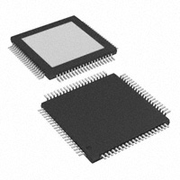
TUSB8040PFP
NRND
HTQFP
PFP
80
RoHS & Green
NIPDAU
Level-3-260C-168 HR
96
Call TI
0 to 70
TUSB8040
(1)
The marketing status values are defined as follows:
ACTIVE: Product device recommended for new designs.
LIFEBUY: TI has announced that the device will be discontinued, and a lifetime-buy period is in effect.
NRND: Not recommended for new designs. Device is in production to support existing customers, but TI does not recommend using this part in a new design.
PREVIEW: Device has been announced but is not in production. Samples may or may not be available.
OBSOLETE: TI has discontinued the production of the device.
(2)
RoHS: TI defines "RoHS" to mean semiconductor products that are compliant with the current EU RoHS requirements for all 10 RoHS substances, including the requirement that RoHS substance
do not exceed 0.1% by weight in homogeneous materials. Where designed to be soldered at high temperatures, "RoHS" products are suitable for use in specified lead-free processes. TI may
reference these types of products as "Pb-Free".
RoHS Exempt: TI defines "RoHS Exempt" to mean products that contain lead but are compliant with EU RoHS pursuant to a specific EU RoHS exemption.
Green: TI defines "Green" to mean the content of Chlorine (Cl) and Bromine (Br) based flame retardants meet JS709B low halogen requirements of


 工商网监
湘ICP备2023018690号
工商网监
湘ICP备2023018690号
