Product
Folder
Sample &
Buy
Support &
Community
Tools &
Software
Technical
Documents
Reference
Design
TUSB9261
SLLSE67I – MARCH 2011 – REVISED MARCH 2016
TUSB9261 USB 3.0 to SATA Bridge
1 Features
2 Applications
•
•
•
•
•
The TUSB9261 is an ARM® Cortex® M3
microcontroller based USB 3.0 to serial ATA bridge. It
provides the necessary hardware and firmware to
implement a USB attached SCSI protocol (UASP)compliant mass storage device suitable for bridging
hard disk drives (HDD), solid state disk drives (SSD),
optical drives, and other compatible SATA 1.5-Gbps
or SATA 3.0-Gbps devices to a USB 3.0 bus. In
addition to UASP support, the firmware implements
the mass storage class BOT and USB HID interfaces.
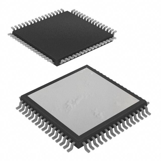
Device Information(1)
PART NUMBER
TUSB9261
PACKAGE
BODY SIZE (NOM)
HTQFP (64)
7.00 × 7.00 mm
(1) For all available packages, see the orderable addendum at
the end of the data sheet.
Simplified Schematic
ROM
GRSTz
ARM
Cortex M3
VDD3.3
RAM
64 kB
VDD1.1
TCK
TMS
TDO
TDI
TRST
JTAG
Data Path
RAM
80 kB
XI
Clock
Generation
Power
and
Reset
Distribution
USB 3.0
Device
Controller
X0
SATA
AHCI
Watchdog
Timer
Timer
DP/DM
USB_R1
USB HS/FS
PHY
VBUS
SSTX+
SSTX-
USB SS
PHY
SSRX+
SSRX-
SATATX+
SATATX-
SATA II
PHY
SATARX+
SATARX-
CS[2:0]
SCLK
DATA_IN
PWM[1:0]
GPIO
PWM
SPI
GPIO[11:0]
SCI
(UART)
USB_R1RTN
•
3 Description
DATA_OUT
•
External HDD/SSD
External DVD
External CD
HDD-Based Portable Media Player
UartTX
•
Universal Serial Bus (USB)
– SuperSpeed USB 3.0 Compliant – TID
340730020
– Integrated Transceiver Supports SS/HS/FS
Signaling
– Best-in-Class Adaptive Equalizer
– Allows for Greater Jitter Tolerance in the
Receiver
– USB Class Support
– USB Attached SCSI Protocol (UASP)
– USB Mass Storage Class Bulk-Only
Transport (BOT)
– Support for Error Conditions Per the 13
Cases (Defined in the BOT Specification)
– USB Bootability Support
– USB Human Interface Device (HID)
– Supports Firmware Update Via USB, Using a
TI Provided Application
SATA Interface
– Serial ATA Specification Revision 2.6
– Gen1i, Gen1m, Gen2i, and Gen2m
– Support for Mass-Storage Devices Compatible
With the ATA/ATAPI-8 Specification
Integrated ARM Cortex M3 Core
– Customizable Application Code Loaded from
EEPROM by SPI Interface
– Two Additional SPI Port Chip Selects for
Peripheral Connection
– Up to 12 GPIOs for End-User Configuration
– Two GPIOs have PWM Functionality for
LED Blink Speed Control
– Serial Communications Interface for Debug
(UART)
General Features
– Integrated Spread Spectrum Clock Generation
Enables Operation from a Single Low-Cost
Crystal or Clock Oscillator
– Supports 40 MHz
– A JTAG Interface is Used for IEEE1149.1 and
IEEE1149.6 Boundary Scan
– Available in a Fully RoHS-Compliant Package
UartRX
1
1
An IMPORTANT NOTICE at the end of this data sheet addresses availability, warranty, changes, use in safety-critical applications,
intellectual property matters and other important disclaimers. PRODUCTION DATA.
�TUSB9261
SLLSE67I – MARCH 2011 – REVISED MARCH 2016
www.ti.com
Table of Contents
1
2
3
4
5
6
7
Features ..................................................................
Applications ...........................................................
Description .............................................................
Revision History.....................................................
Pin Configuration and Functions .........................
Specifications.........................................................
1
1
1
2
3
7
6.1
6.2
6.3
6.4
6.5
6.6
6.7
6.8
6.9
7
7
7
7
8
8
8
9
9
Absolute Maximum Ratings ......................................
ESD Ratings..............................................................
Recommended Operating Conditions.......................
Thermal Information ..................................................
DC Electrical Characteristics for 3.3-V Digital I/O.....
SuperSpeed USB Power Consumption ....................
High-Speed USB Power Consumption .....................
Oscillator Specification..............................................
Crystal Specification..................................................
Detailed Description ............................................ 10
7.1 Overview ................................................................. 10
7.2 Functional Block Diagram ....................................... 10
7.3 Feature Description................................................. 10
7.4 Device Functional Modes........................................ 13
8
Application and Implementation ........................ 15
8.1 Application Information............................................ 15
8.2 Typical Application .................................................. 15
9
Power Supply Recommendations...................... 19
9.1 Digital Supplies 1.1-V and 3.3-V ............................. 19
9.2 Analog Supplies 1.1-V and 3.3-V ........................... 19
10 Layout................................................................... 19
10.1 Layout Guidelines ................................................. 19
10.2 Layout Examples................................................... 20
11 Device and Documentation Support ................. 22
11.1
11.2
11.3
11.4
Community Resources..........................................
Trademarks ...........................................................
Electrostatic Discharge Caution ............................
Glossary ................................................................
22
22
22
22
12 Mechanical, Packaging, and Orderable
Information ........................................................... 22
4 Revision History
NOTE: Page numbers for previous revisions may differ from page numbers in the current version.
Changes from Revision H (July 2015) to Revision I
•
Page
Changed the CDM value in the ESD Ratings table From: 5000 To: ±1500 .......................................................................... 7
Changes from Revision G (October 2014) to Revision H
Page
•
Moved Tstg from Handling Ratings table to Absolute Maximum Ratings and renamed Handling Ratings to ESD Ratings ... 7
•
Updated the frequency for the USB2 and USB3 to 5 Hz and 10 Hz, respectively ............................................................. 16
Changes from Revision F (March 2014) to Revision G
Page
•
Updated supported frequency to 40 MHz .............................................................................................................................. 1
•
Updated supported frequency in Clock and Reset Signals table .......................................................................................... 4
•
Updated the frequency for the clock to 40 MHz .................................................................................................................... 9
•
Updated the frequency for the crystal to 40 MHz .................................................................................................................. 9
•
Updated oscillation frequency and ESR equivalent series resistance .................................................................................. 9
•
Updated Table 1 ................................................................................................................................................................... 12
2
Submit Documentation Feedback
Copyright © 2011–2016, Texas Instruments Incorporated
Product Folder Links: TUSB9261
�TUSB9261
www.ti.com
SLLSE67I – MARCH 2011 – REVISED MARCH 2016
5 Pin Configuration and Functions
PVP Package
48-Pin HTQFP
Top View
VDD
VDDA33
USB_DM
USB_DP
NC
USB_R1
USB_R1RTN
VDDA33
VDD
USB_SSTXM
USB_SSTXP
VSS
USB_SSRXM
USB_SSRXP
VDD
VDDA33
48 47 46 45 44 43 42 41 40 39 38 37 36 35 34 33
VDD
USB_VBUS
VDD33
XI
VSSOSC
XO
VDD
SATA_TXM
SATA_TXP
VSS
SATA_RXM
SATA_RXP
VDD
VDDA33
VDD
NC
49
50
51
52
53
54
55
56
57
58
59
60
61
62
63
64
65
VSS
32
31
30
29
28
27
26
25
24
23
22
21
20
19
18
17
VDD
FREQSEL1
FREQSEL0
JTAG_TRSTz
JTAG_TMS
JTAG_TDO
JTAG_TDI
JTAG_TCK
VDD33
SPI_CS2 / GPIO11
SPI_CS1 / GPIO10
SPI_CS0
SPI_DATA_IN
VDD
SPI_DATA_OUT
SPI_SCLK
1 2 3 4 5 6 7 8 9 10 11 12 13 14 15 16
GPIO7
GPIO6
GPIO5
GPIO4
VDD
GPIO3
GPIO2
GPIO1
GPIO0
VDD33
GPIO9 / UART_TX
GPIO8 / UART_RX
GRSTz
PWM1
PWM0
VDD
Submit Documentation Feedback
Copyright © 2011–2016, Texas Instruments Incorporated
Product Folder Links: TUSB9261
3
�TUSB9261
SLLSE67I – MARCH 2011 – REVISED MARCH 2016
www.ti.com
Signal Descriptions – I/O Definitions
I/O TYPE
DESCRIPTION
I
Input
O
Output
I/O
Input/output
PU
Internal pullup resistor
PD
Internal pulldown resistor
PWR
Power signal
Clock and Reset Signals
PIN
NAME
NO.
I/O
DESCRIPTION
GRSTz
4
I
PU
XI
52
I
Crystal input. This terminal is the crystal input for the internal oscillator. The input may alternately
be driven by the output of an external oscillator. When using a crystal, a 1-MΩ feedback resistor
is required between X1 and XO.
XO
54
O
Crystal output. This terminal is the crystal output for the internal oscillator. If XI is driven by an
external oscillator, this pin may be left unconnected. When using a crystal, a 1-MΩ feedback
resistor is required between X1 and XO.
31, 30
I
PU
FREQSEL[1:0]
Global power reset. This reset brings all of the TUSB9261 internal registers to their default
states. When GRSTz is asserted, the device is completely nonfunctional.
Frequency select. These terminals indicate the oscillator input frequency and are used to
configure the correct PLL multiplier. The field encoding is as follows:
FREQSEL[1]
FREQSEL[0]
INPUT CLOCK FREQUENCY
1
1
40 MHz
SATA Interface Signals (1)
PIN
NAME
NO.
I/O
DESCRIPTION
SATA_TXP
57
O
Serial ATA transmitter differential pair (positive)
SATA_TXM
56
O
Serial ATA transmitter differential pair (negative)
SATA_RXP
60
I
Serial ATA receiver differential pair (positive)
SATA_RXM
59
I
Serial ATA receiver differential pair (negative)
(1)
Note that the default firmware and reference design for the TUSB9261 have the SATA TXP/TXM swapped for ease of routing in the
reference design. If you plan to use the TI default firmware please review the reference design in the TUSB9261 DEMO User’s Guide
(SLLU139) for proper SATA connection.
USB Interface Signals
PIN
NAME
NO.
I/O
DESCRIPTION
USB_SSTXP
43
O
SuperSpeed USB transmitter differential pair (positive)
USB_SSTXM
42
O
SuperSpeed USB transmitter differential pair (negative)
USB_SSRXP
46
I
SuperSpeed USB receiver differential pair (positive)
USB_SSRXM
45
I
SuperSpeed USB receiver differential pair (negative)
USB_DP
36
I/O
USB high-speed differential transceiver (positive)
USB_DM
35
I/O
USB high-speed differential transceiver (negative)
USB_VBUS
50
I
USB bus power
USB_R1
38
O
Precision resistor reference. A 10-kΩ ±1% resistor should be connected between R1 and R1RTN.
USB_R1RTN
39
I
Precision resistor reference return
4
Submit Documentation Feedback
Copyright © 2011–2016, Texas Instruments Incorporated
Product Folder Links: TUSB9261
�TUSB9261
www.ti.com
SLLSE67I – MARCH 2011 – REVISED MARCH 2016
Serial Peripheral Interface (SPI) Signals
PIN
NAME
NO.
I/O
DESCRIPTION
SPI_SCLK
17
O
PU
SPI clock
SPI_DATA_OUT
18
O
PU
SPI master data out
SPI_DATA_IN
20
I
PU
SPI master data in
SPI_CS0
21
O
PU
Primary SPI chip select for flash RAM
23
I/O
PU
SPI chip select for additional peripherals. When not used for SPI chip select, this pin may be used
as a general-purpose I/O.
22
I/O
PU
SPI chip select for additional peripherals. When not used for SPI chip select, this pin may be used
as a general-purpose I/O.
SPI_CS2/
GPIO11
SPI_CS1/
GPIO10
JTAG, GPIO, and PWM Signals
PIN
NAME
NO.
I/O
DESCRIPTION
JTAG_TCK
25
I
PD
JTAG test clock
JTAG_TDI
26
I
PU
JTAG test data in
JTAG_TDO
27
O
PD
JTAG test data out
JTAG_TMS
28
I
PU
JTAG test mode select
JTAG_TRSTz
29
I
PD
JTAG test reset
GPIO9/UART_TX
6
I/O
PU
GPIO/UART transmitter. This terminal can be configured as a GPIO or as the transmitter for a
UART channel. This pin defaults to a general-purpose output.
GPIO8/UART_RX
5
I/O
PU
GPIO/UART receiver. This terminal can be configured as a GPIO or as the receiver for a UART
channel. This pin defaults to a general-purpose output.
GPIO7
16
I/O
PD
GPIO6
15
I/O
PD
GPIO5
14
I/O
PD
GPIO4
13
I/O
PD
GPIO3
11
I/O
PD
GPIO2
10
I/O
PD
GPIO1
9
I/O
PD
GPIO0
8
I/O
PD
PWM0
2
O
PD (1)
PWM1
3
O
PD (1)
(1)
Configurable as general-purpose input/outputs
Pulse-width modulation (PWM). Can be used to drive status LEDs.
PWM pulldown resistors are disabled by default. A firmware modification is required to turn them on. All other internal pull up/down
resistors are enabled by default.
Submit Documentation Feedback
Copyright © 2011–2016, Texas Instruments Incorporated
Product Folder Links: TUSB9261
5
�TUSB9261
SLLSE67I – MARCH 2011 – REVISED MARCH 2016
www.ti.com
Power and Ground Signals
PIN
NAME
NO.
I/O
DESCRIPTION
1
12
19
32
33
VDD
41
PWR
1.1-V power rail
PWR
3.3-V power rail
PWR
3.3-V analog power rail
PWR
Oscillator ground. If using a crystal, this should not be connected to a PCB ground plane. If
using an oscillator, this should be connected to PCB ground. See Clock Source Requirements
for more details.
PWR
Ground
PWR
Ground – Thermal pad
47
49
55
61
63
7
VDD33
24
51
34
VDDA33
40
48
62
VSSOSC
VSS
VSS
NC
6
53
44
58
65
37
64
—
No connect, leave floating
Submit Documentation Feedback
Copyright © 2011–2016, Texas Instruments Incorporated
Product Folder Links: TUSB9261
�TUSB9261
www.ti.com
SLLSE67I – MARCH 2011 – REVISED MARCH 2016
6 Specifications
6.1 Absolute Maximum Ratings
over operating free-air temperature (unless otherwise noted)
MIN
MAX
UNIT
VDD
Steady-state supply voltage
–0.3
1.4
V
VDD33/
VDDA33
Steady-state supply voltage
–0.3
3.8
V
Tstg
Storage temperature
–55
150
°C
6.2 ESD Ratings
VALUE
VESD
(1)
(2)
Electrostatic discharge
Human body model (HBM), per ANSI/ESDA/JEDEC JS001
(1)
UNIT
±2000
Charged device model (CDM), per JESD22-C101 (2)
V
±1500
JEDEC document JEP155 states that 500-V HBM allows safe manufacturing with a standard ESD control process.
JEDEC document JEP157 states that 250-V CDM allows safe manufacturing with a standard ESD control process.
6.3 Recommended Operating Conditions
over operating free-air temperature range (unless otherwise noted)
MIN
NOM
MAX
UNIT
VDD
Digital 1.1-V supply voltage
1.045
1.1
1.155
V
VDD33
Digital 3.3-V supply voltage
3
3.3
3.6
V
VDDA33
Analog 3.3-V supply voltage
3
3.3
3.6
V
VBUS
Voltage at VBUS PAD
0
1.155
V
0
70
–40
85
–40
100
TA
Operating free-air temperature range
TJ
Operating junction temperature range
Industrial version
°C
°C
6.4 Thermal Information
TUSB9261
THERMAL METRIC (1)
PVP (HTQFP)
UNIT
64 PINS
RθJA
Junction-to-ambient thermal resistance
30.2
°C/W
RθJC(top)
Junction-to-case (top) thermal resistance
11.0
°C/W
RθJB
Junction-to-board thermal resistance
6.1
°C/W
ψJT
Junction-to-top characterization parameter
0.4
°C/W
ψJB
Junction-to-board characterization parameter
6.1
°C/W
RJθC(bot)
Junction-to-case (bottom) thermal resistance
0.9
°C/W
(1)
For more information about traditional and new thermal metrics, see the Semiconductor and IC Package Thermal Metrics application
report, SPRA953.
Submit Documentation Feedback
Copyright © 2011–2016, Texas Instruments Incorporated
Product Folder Links: TUSB9261
7
�TUSB9261
SLLSE67I – MARCH 2011 – REVISED MARCH 2016
www.ti.com
6.5 DC Electrical Characteristics for 3.3-V Digital I/O
over operating free-air temperature range (unless otherwise noted)
PARAMETER
TEST CONDITIONS
MIN
TYP
MAX
UNIT
DRIVER
TR
Rise time
5 pF
1.5
TF
Fall time
5 pF
1.53
IOL
Low-level output current
VDD33 = 3.3 V, TJ = 25°C
6
IOH
High-level output current
VDD33 = 3.3 V, TJ = 25°C
–6
VOL
Low-level output voltage
IOL = 2 mA
VOH
High-level output voltage
IOL = –2 mA
VO
Output voltage
ns
ns
mA
mA
0.4
2.4
V
V
0
VDD33
V
RECEIVER
VI
Input voltage
0
VDD33
V
VIL
Low-level input voltage
0
0.8
V
VIH
High-level input voltage
2
Vhys
Input hysteresis
tT
Input transition time (TR and TF)
II
Input current
VI = 0 V to VDD33
CI
Input capacitance
VDD33 = 3.3 V, TJ = 25°C
V
200
mV
0.384
10
ns
5
µA
pF
6.6 SuperSpeed USB Power Consumption
POWER RAIL
TYPICAL ACTIVE CURRENT (mA) (1)
TYPICAL SUSPEND CURRENT (mA) (2)
VDD11
291
153
65
28
VDD33
(1)
(2)
(3)
(3)
Transferring data by SS USB to a SSD SATA Gen II device. No SATA power management, U0 only.
SATA Gen II SSD attached no active transfer. No SATA power management, U3 only.
All 3.3-V power rails connected together.
6.7 High-Speed USB Power Consumption
(1)
(2)
(3)
8
POWER RAIL
TYPICAL ACTIVE CURRENT (mA) (1)
TYPICAL SUSPEND CURRENT (mA) (2)
VDD11
172
153
VDD33 (3)
56
28
Transferring data via HS USB to a SSD SATA Gen II device. No SATA power management.
SATA Gen II SSD attached no active transfer. No SATA power management.
All 3.3-V power rails connected together.
Submit Documentation Feedback
Copyright © 2011–2016, Texas Instruments Incorporated
Product Folder Links: TUSB9261
�TUSB9261
www.ti.com
SLLSE67I – MARCH 2011 – REVISED MARCH 2016
6.8 Oscillator Specification
XI should be tied to the 1.8-V clock source and XO should be left floating. VSSOSC should be connected to the PCB ground
plane. A 40-MHz clock can be used.
PARAMETER
TEST CONDITIONS
MIN
TYP
UNIT
XI input capacitance
VIL
Low-level input voltage
VIH
High-level input voltage
Ttosc_i
Frequency tolerance
Tduty
Duty cycle
TR/TF
Rise/fall time
20% to 80%
6
ns
RJ
Reference clock
JTF (1 sigma) (1) (2)
0.8
ps
TJ
Reference clock
JTF (total p-p) (2) (3)
25
ps
50
ps
Tp-p
(1)
(2)
(3)
(4)
Reference clock jitter
TJ = 25°C
MAX
CXI
0.414
pF
0.7
V
50
ppm
1.05
Operational temperature
V
–50
45%
(Absolute p-p)
50%
55%
(4)
Sigma value assuming Gaussian distribution
After application of JTF
Calculated as 14.1 × RJ + DJ
Absolute phase jitter (p-p)
6.9 Crystal Specification
A parallel, 20-pF load capacitor should be used if a crystal source is used. VSSOSC should not be connected to the PCB
ground plane. A 40-MHz crystal can be used.
PARAMETER
TEST CONDITIONS
MIN
Oscillation mode
TYP
MAX
UNIT
Fundamental
ƒO
Oscillation frequency
ESR
Equivalent series resistance
40 MHz
40
Ttosc_i
Frequency tolerance
Frequency stability
MHz
50
Ω
Operational temperature
±50
ppm
1 year aging
±50
ppm
24
pF
CL
Load capacitance
CSHUNT
Crystal and board stray capacitance
12
20
4.5
pF
Drive level (max)
0.8
mW
Submit Documentation Feedback
Copyright © 2011–2016, Texas Instruments Incorporated
Product Folder Links: TUSB9261
9
�TUSB9261
SLLSE67I – MARCH 2011 – REVISED MARCH 2016
www.ti.com
7 Detailed Description
7.1 Overview
The major functional blocks are as follows:
• Cortex M3 microcontroller subsystem including the following peripherals:
– Time interrupt modules, including watchdog timer
– Universal asynchronous receive/transmit (SCI)
– SPI
– General purpose input/output (GPIO)
– PWM for support of PWM outputs (PWM)
• USB 3.0 core (endpoint controller) and integrated USB 3.0 PHY
• AHCI-compliant SATA controller and integrated SATA PHY
– Supporting Gen1i, Gen1m, Gen2i, and Gen2m
• Chip level clock generation and distribution
• Support for JTAG 1149.1 and 1149.6
7.2 Functional Block Diagram
USB 3.0
(1)
SuperSpeed
PC
with
USB 3.0
Support
SATA
Gen1/2
HDD
USB 2.0
(1)
High-speed
TUSB9260
TUSB9261
A.
USB connection is made at either SuperSpeed or high speed, depending on the upstream connection support.
7.3 Feature Description
7.3.1 Operation
7.3.1.1 General Functionality
The TUSB9261 ROM contains boot code that executes after a global reset, which performs the initial
configuration required to load a firmware image from an attached SPI flash memory to local RAM.
After the firmware is loaded, it configures the SATA advanced host controller interface host bus adapter (AHCI)
and the USB device controller. In addition, the configuration of the AHCI includes a port reset, which initiates an
out of band (OOB) TX sequence from the AHCI link layer to determine if a device is connected, and if so,
negotiate the connection speed with the device (3.0 Gbps or 1.5 Gbps).
The configuration of the USB device controller includes creation of the descriptors, configuration of the device
endpoints for support of UASP and USB mass storage class BOT, allocation of memory for the transmit request
blocks (TRBs), and creation of the TRBs necessary to transmit and receive packet data over the USB. In
addition, the firmware provides any other custom configuration required for application-specific implementation,
for example, a HID interface for user initiated backup.
10
Submit Documentation Feedback
Copyright © 2011–2016, Texas Instruments Incorporated
Product Folder Links: TUSB9261
�TUSB9261
www.ti.com
SLLSE67I – MARCH 2011 – REVISED MARCH 2016
Feature Description (continued)
After the USB device controller configuration is complete, if a SATA device was detected during the AHCI
configuration, the firmware connects the device to the USB bus when VBUS is detected. According to the USB
3.0 specification, the TUSB9261 initially tries to connect at SuperSpeed USB. If successful, it enters U0;
otherwise, after the training time out, it enables the DP pullup and connects as a USB 2.0 high-speed or fullspeed device depending on the speed supported by host or hub port.
When connected, the firmware presents the BOT interface as the primary interface and the UASP interface as
the secondary interface. If the host stack is UASP aware, it can enable the UASP interface using a
SET_INTERFACE request for alternate interface 1.
Following speed negotiation, the device should transmit a device to host (D2H) FIS with the device signature.
This first D2H FIS is received by the link layer and copied to the port signature register. When firmware is notified
of the device connection, it queries the device for capabilities using the IDENTIFY DEVICE command. Firmware
then configures the device as appropriate for its interface and features supported, for example, an HDD that
supports native command queuing (NCQ).
7.3.1.2 Firmware Support
Default firmware support is provided for the following:
• SuperSpeed USB and USB 2.0 high speed and full speed
• USB attached SCSI protocol (UASP)
• USB mass storage class (MSC) bulk-only transport (BOT)
– Including the 13 error cases
• USB mass storage specification for bootability
• USB device class definition for HID
– Firmware update and custom functionality (for example, one-touch backup)
• Serial ATA advanced host controller interface (AHCI)
• GPIO
– LED control and custom functions (for example, one-touch backup control)
• PWM
– LED dimming control
• SPI
– Firmware storage and storing custom device descriptors
• Serial communications interface (SCI)
– Debug output only
Submit Documentation Feedback
Copyright © 2011–2016, Texas Instruments Incorporated
Product Folder Links: TUSB9261
11
�TUSB9261
SLLSE67I – MARCH 2011 – REVISED MARCH 2016
www.ti.com
Feature Description (continued)
7.3.1.3 GPIO/PWM LED Designations
The default firmware provided by TI drives the GPIO and PWM outputs as listed in Table 1.
Table 1. GPIO/PWM LED Designations
GPIO
DESCRIPTION
DEFAULT
SETUP
GPIO0
Undefined. Can use HID commands to change to output low or high.
[internal 100-µA PD]
Input
GPIO1
USB 3.0 Link State if U1/U2 enabled, otherwise [input with 100-µA PD]
Output
GPIO5
USB 3.0 Link State if U1/U2 enabled, otherwise [input with 100-µA PD]
Output
U0: Off/Off
U1: On/Off
GPIO1/
GPIO5
USB3 power state (U0 to U3) U2: Off/On
Output
U3: On/On
Other: Off/Off
GPIO2
HS/FS suspend
Output
GPIO3
[INPUT with 100-µA PD] momentary push button
Input
GPIO4
Bus- or self-powered indicator. (GPIO level should be HIGH when selfpowered). [internal 100-µA PD]
Input
GPIO6
Undefined. Can use HID commands to change to output low or high.
[internal 100-µA PD]
Input
GPIO7
SS connection
Output
GPIO10
Undefined. Can use HID commands to change to output low or high.
Compile option to configure as SATA drive power enable output.
[internal 100-µA PU]
Input
GPIO11
Power fault indicator. [internal 100-µA PU]
Input
PWM0
Disk activity (LED blink rate is faster when connected at USB
SuperSpeed), USB connection (LED on), and USB suspend (fading
LED).
Output
PWM1
SW heartbeat
Output
The LEDs on the TUSB9261 product development kit (PDK) board are connected as in Table 1. See the
TUSB9261 PDK Guide for more information on GPIO LED connection and usage. This EVM is available for
purchase. Contact TI for ordering information.
7.3.1.4 Power-Up and Reset Sequence
The core power (VDD) must be present and at its minimum high level prior to, or at the same time that, the I/O
power (VDD33).
In addition, meet the following constraints:
• All maximum ratings and recommended operating conditions are observed.
• All warnings about exposure to maximum rated and recommended conditions are observed, particularly
junction temperature. These apply to power transitions as well as normal operation.
• Bus contention while VDD33 is powered up must be limited to 100 hours over the projected lifetime of the
device.
• Bus contention while VDD33 is powered down may violate the absolute maximum ratings.
A supply bus is powered up when the voltage is within the recommended operating range. It is powered down
when it is below that range, either stable or in transition.
A minimum reset duration of 2 ms is required. This is defined as the time when the power supplies are in the
recommended operating range to the deassertion of GRSTz.
12
Submit Documentation Feedback
Copyright © 2011–2016, Texas Instruments Incorporated
Product Folder Links: TUSB9261
�TUSB9261
www.ti.com
SLLSE67I – MARCH 2011 – REVISED MARCH 2016
7.3.2 Clock Connections
7.3.2.1 Clock Source Requirements
The TUSB9261 supports an external oscillator source or a crystal unit. If a clock is provided to XI instead of a
crystal, XO is left open and VSSOSC should be connected to the PCB ground plane. Otherwise, if a crystal is
used, the connection needs to follow these guidelines.
Because XI and XO are coupled to other leads and supplies on the PCB, it is important to keep them as short as
possible and away from any switching leads. TI also recommends to minimize the capacitance between XI and
XO. This can be accomplished by connecting the VSSOSC lead to the two external capacitors CL1 and CL2 and
shielding them with the clean ground lines. The VSSOSC should not be connected to PCB ground when using a
crystal.
Load capacitance (Cload) of the crystal (varies with the crystal vendor) is the total capacitance value of the entire
oscillation circuit system as seen from the crystal. It includes two external capacitors, CL1 and CL2, in Figure 1.
The trace length between the decoupling capacitors and the corresponding power pins on the TUSB9261 must
be minimized. TI also recommends that the trace length from the capacitor pad to the power or ground plane be
minimized.
CL1
XI
VSSOSC
Crystal
XO
CL2
Figure 1. Typical Crystal Connections
7.3.2.2 Clock Source Selection Guide
Reference clock jitter is an important parameter. Jitter on the reference clock degrades both the transmit eye and
receiver jitter tolerance no matter how clean the rest of the PLL is, thereby impairing system performance.
Additionally, a particularly jittery reference clock may interfere with the PLL lock detection mechanism, forcing the
lock detector to issue an Unlock signal. A good-quality, low-jitter reference clock is required to achieve
compliance with supported USB3.0 standards. For example, USB3.0 specification requires the random jitter (RJ)
component of either RX or TX to be 2.42 ps (random phase jitter calculated after applying jitter transfer function
(JTF)). As the PLL typically has a number of additional jitter components, the reference clock jitter must be
considerably below the overall jitter budget.
7.4 Device Functional Modes
7.4.1 VBUS Power
Power can be supplied by a USB cable on the terminal VBUS. When using power from VBUS, both the
TUSB9261 and the SATA device are allowed to draw only up to 500 mA from VBUS when operating.
7.4.2 External Power
Power can be supplied from an external power source. When using an external power source, both the
TUSB9261 and the SATA interface can draw all their current from the external supply.
Submit Documentation Feedback
Copyright © 2011–2016, Texas Instruments Incorporated
Product Folder Links: TUSB9261
13
�TUSB9261
SLLSE67I – MARCH 2011 – REVISED MARCH 2016
www.ti.com
Device Functional Modes (continued)
7.4.3 External Voltage Regulator
Because the TUSB9261 requires two voltage supplies (1.1 V and 3.3 V), TI recommends a multi-channel voltage
regulator. The TPS650061 or TPS65024x are good choices. The TPS650061 uses a DC-DC converter and two
LDO regulators in a single package. The DC-DC converter can supply 1-A nominal current while the two LDOs
can supply 300-mA nominal current. Because the 1.1-V supply can consume upwards of 340 mA of current, the
DC-DC converter is ideal for supplying the 1.1-V current while the two LDOs can be used to supply 3.3-V current.
Likewise the TPS65024x uses three DC-DC converters and three LDOs. Both devices also have a built-in
supervisor circuit that can be connected to GRST on the TUSB9261.
14
Submit Documentation Feedback
Copyright © 2011–2016, Texas Instruments Incorporated
Product Folder Links: TUSB9261
�TUSB9261
www.ti.com
SLLSE67I – MARCH 2011 – REVISED MARCH 2016
8 Application and Implementation
NOTE
Information in the following applications sections is not part of the TI component
specification, and TI does not warrant its accuracy or completeness. TI’s customers are
responsible for determining suitability of components for their purposes. Customers should
validate and test their design implementation to confirm system functionality.
8.1 Application Information
The device serves as a bridge between a downstream USB 3.0 host port and a SATA device such as a hard disk
drive. A crystal or oscillator supplies the required clock source. A SPI flash device contains the firmware that is
loaded into the TUSB9261 after the deassertion of RESET. Push buttons or any other desired logic can be
connected to the TUSB9261 GPIO pins. The TUSB9261 can also output a pulse-width modulated signal that can
be used to drive an activity LED.
8.2 Typical Application
Optional
JTAG
Header
SPI
FLASH
TUSB9261
SPI
JTAG
USB 3.0
SuperSpeed
SATA
Gen 1/2
PC with
USB 3.0
Support
Serial ATA Device
USB 2.0
High-speed
CLOCK
GPIO/PWM
HDD
Activity
LED
Crystal or
Oscillator
Figure 2. Typical Application Schematic
8.2.1 Design Requirements
Table 2. Design Parameters
DESIGN PARAMETER
EXAMPLE VALUE
VDD supply
1.1 V
VDD33 supply
3.3 V
Upstream port USB support
SS, HS, FS
Main supply
VBUS
USB_VBUS resistor values
90.9 kΩ, 10 kΩ
Crystal frequency
40 MHz
SATA device
SSD
Submit Documentation Feedback
Copyright © 2011–2016, Texas Instruments Incorporated
Product Folder Links: TUSB9261
15
�TUSB9261
SLLSE67I – MARCH 2011 – REVISED MARCH 2016
www.ti.com
8.2.2 Detailed Design Procedure
8.2.2.1 PWM Terminals
The TUSB9261 has two pulse-width modulated output terminals.
Table 3 shows the default firmware configuration of PWMs.
Table 3. Default Firmware Configuration of PWMs
PWM
USAGE
0
Primary Indicator LED:
ON when there is a USB connection. OFF when there is no connection.
Blinks during disk activity (Frequency: 5 Hz for USB2 or 10 Hz for USB3).
Fades when USB is in Suspend or U3 state.
1
Power indicator LED
PWM duty cycle will be 0% when the LED should be fully ON.
8.2.2.2 JTAG Interface
The TUSB9261 supports JTAG for board-level test and debug support. Typically, these terminals are left
unconnected or routed to a header to plug in an external JTAG controller. Table 4 shows the JTAG terminal
names and internal resistor connection. The JTAG interface should be left unconnected if JTAG support is not
required.
Table 4. Internal JTAG Resistor Termination
NAME
PULL UP OR PULL
DOWN
DESCRIPTION
JTAG_TCK
Pull down
JTAG test clock
JTAG_TDI
Pull up
JTAG test data in
JTAG_TDO
Pull down
JTAG test data out
JTAG_TMS
Pull up
JTAG test mode select
JTAG_RSTZ
Pull down
JTAG reset
8.2.2.3 Voltage Regulator Schematic
VDD_1P1V
L2
2.2 µH
R30 0402
BOARD_5V
400 kΩ 1%
R31
475 kΩ
0402
1%
U4
MODE
C57
22 µF
8
10
9
R39
1
19
MR#
4.7 kΩ
0402
15
3
18
4
SW2
PB_SWITCH
1
2
4
3
N.O.
A
VINDCDC
EN_DCDC
MODE
MR#
RSTSNS
VINLDO1
EN_LDO1
VINLDO2
EN_LDO2
SW
FB_DCDC
PG#
TRST
RST#
VLDO1
FB_LDO1
PGND
VLDO2
FB_LDO2
AGND
PWR_PAD
TPS650061
STAR GROUND AGND TO GND
7
11
5
SW_1.1V
FB_DCDC
2
20
TRST
30 pF
A
R32
BOARD_3P3V
GRST#
14
13
6
17
16
12
21
C46
22 µF
C72
BOARD_1P8V
4.7 kΩ
0402
5%
C60
22 µF
C68
0.1 µF
A
A
C63
22 µF
A
8.2.2.4 SPI
A SPI system consists of one master device and one or more slave devices. The TUSB9261 is a SPI master
providing the SPI clock, data-in, data-out, and up to three chip-select terminals.
16
Submit Documentation Feedback
Copyright © 2011–2016, Texas Instruments Incorporated
Product Folder Links: TUSB9261
�TUSB9261
www.ti.com
SLLSE67I – MARCH 2011 – REVISED MARCH 2016
The SPI has a 4-wire synchronous serial interface. Data communication is enabled with an active-low chip select
terminal (SPI_CS[2:0]#). Data is transmitted with a 3-terminal interface consisting of terminals for serial data
input (SPI_DATA_IN), serial data output (SPI_DATA_OUT) and serial clock (SPI_SCLK).
All SPI terminals have integrated pullup resistors. No external components are required to connect the SPI
interface to an external SPI flash device. See Figure 3 for an example implementation of the SPI interface using
one SPI slave device.
BOARD_3P3V
R2
4.7K
TUSB9261
R3
4.7K
U2
1
2
3
4
CE#
SO
WP#
GND
VCC
HOLD#
SCK
SI
8
7
6
5
Pm25LV512A
SPI_SO_J
SPI_SCLK
SPI_DATA_OUT
SPI_DATA_IN
SPI_CS0
17
18
20
21
SPI_SCK
SPI_SO
SPI_SI
SPI_CE#
SOIC_8S
C11
0.1uF
J13
1
2
SPI ENABLE
HDR2X1 M .1
Figure 3. SPI Connection
The SPI_CLK is running at a fixed frequency of 18.75 MHz and its clocking mode is configured with a POLARITY
of 0 and a PHASE of 1, this means that the SPI sends the data output one half-cycle before the first rising edges
of SPI_CLK and on subsequent falling edges. Meanwhile, the input data is latched on the rising edge of
SPI_CLK (see Figure 4 and Table 5 for a detailed timing description).
The flash memory is erased by the bootloader prior to programming and must use a word size of 8 bits with an
address length of 24 bits and its program instruction must allow 256 bytes to be written in one operation. TI
recommends a minimum flash size of 512 kb (64 k × 8). Table 5 shows SPI flash devices that have been tested
with the TUSB9261.
Figure 4. SPI Characterization
Submit Documentation Feedback
Copyright © 2011–2016, Texas Instruments Incorporated
Product Folder Links: TUSB9261
17
�TUSB9261
SLLSE67I – MARCH 2011 – REVISED MARCH 2016
www.ti.com
Table 5. SPI Characterization Time
NO.
18
TIME REFERENCE
THEORETICAL VALUE
1
Cycle time SPICLK
53.3 ns
2
Positive SPI_CLK slope
2 ns
3
Negative SPI_CLK slope
3 ns
4
SPISCS – SPICLK edge(PHASE = 1)
MIN: 53.3 ns
TYP: 80 ns
MAX: 93.3 ns
5
Output delay time, SPICLK TX edge to SPISIMO valid
260 ps
6
Output hold time, SPICLK RX edge to SPISIMO valid
26.7 ns
7
Setup time
22 ns
8
Hold time
500 ps
9
"SPICLK -SPISCS Phase = 1, Master"
13.3 ns
Submit Documentation Feedback
Copyright © 2011–2016, Texas Instruments Incorporated
Product Folder Links: TUSB9261
�TUSB9261
www.ti.com
SLLSE67I – MARCH 2011 – REVISED MARCH 2016
9 Power Supply Recommendations
9.1 Digital Supplies 1.1-V and 3.3-V
The TUSB9261 requires a 1.1-V and 3.3-V digital power source.
The 1.1-V terminals are named VDD11. These terminals supply power to the digital core. The 1.1-V core allows
for a significant reduction in both power consumption and logic switching noise.
The 3.3-V terminals are named VDD33 and supply power to most of the input and output cells. Both VDD11 and
VDD33 supplies must have 0.1-μF bypass capacitors to VSS (ground) to ensure proper operation. One capacitor
per power terminal is sufficient and should be placed as close to the terminal as possible to minimize trace
length. TI also recommends smaller value capacitors like 0.01-μF on the digital supply terminals.
When placing and connecting all bypass capacitors, follow high-speed board design rules.
9.2 Analog Supplies 1.1-V and 3.3-V
TI recommends a Pi filter on all analog power terminals to minimize circuit noise. These filters can be combined
on a per-rail basis for a total of two (VDDA11 / VDDA11_USB2) + (VDDA33).
Analog power terminals must have a 1-μF and a 10-μF bypass capacitor connected to VSSA (ground) to ensure
proper operation. Place the capacitor as close as possible to the associated terminal to minimize trace length. TI
also recommends smaller value capacitors such as 0.1-μF and 0.01-μF on the analog supply terminals.
10 Layout
10.1 Layout Guidelines
10.1.1 High-Speed Differential Routing
The high-speed differential pair (USB_DM and USB_DP) is connected to a USB type B connector. The
differential pair traces should be routed with 90-Ω, ±15% differential impedance. The high-speed signal pair
should be trace length matched. Maximum trace length mismatch between high-speed USB signal pairs should
be no greater than 150 mils. Keep total trace length to a minimum. Route differential traces first. Route the
differential pairs on the top or bottom layers with the minimum amount of vias possible. No termination or
coupling capacitors are required. If a common-mode choke is required, then place the choke as close as possible
to the USB connector signal pins. Likewise, ESD clamps should also be placed as close as possible to the USB
connector signal pins (closer than the choke).
To minimize crosstalk on the USB2/3 differential signal pairs, TI recommends that the spacing between the two
interfaces be five times the width of the trace (5W rule). For instance, if the SS USB TX/RX differential pair trace
widths are 5 mils, then there should be 25 mils of space (air gap) between the TX and RX differential pairs and
the DP/DM differential pair. If this 5W rule cannot be implemented, then the space between the TX/RX differential
pairs and DP/DM differential pairs should be maximized as much as possible and ground-fill should be placed
between the two. In this case, it is better to route each differential pair on opposite sides of the board with a
ground plane between them.
10.1.2 SuperSpeed Differential Routing
SuperSpeed consists of two differential routing pairs, a transmit pair (USB_SSTXM and USB_SSTXP) and a
receive pair (USB_SSRXM and USB_SSRXP). Each differential pair’s traces should be routed with 90-Ω, ±15%
differential impedance. The high-speed signal pair should be trace length matched. Maximum trace length
mismatch between SuperSpeed USB signal pairs should be no greater than 2.5 mils. The transmit differential
pair does not have to be the same length as the receive differential pair. Keep total trace length to a minimum.
Route differential traces first. Route the differential pairs on the top or bottom layers with the minimum amount of
vias possible. The transmitter differential pair requires 0.1-uF coupling capacitors for proper operation. The
package/case size of these capacitors should be no bigger than 0402. C-packs are not allowed. The capacitors
should be placed symmetrically as close as possible to the USB connector signal pins. If a common mode choke
is required, then place the choke as close as possible to the USB connector signal pins (closer than the
transmitter capacitors). Likewise ESD clamps should also be placed as close as possible to the USB connector
signal pins (closer than the choke and transmitter capacitors).
Submit Documentation Feedback
Copyright © 2011–2016, Texas Instruments Incorporated
Product Folder Links: TUSB9261
19
�TUSB9261
SLLSE67I – MARCH 2011 – REVISED MARCH 2016
www.ti.com
Layout Guidelines (continued)
It is permissible to swap the plus and minus on either or both of the SuperSpeed differential pairs. This may be
necessary to prevent the differential traces from crossing over one another. However, it is not permissible to
swap the transmitter differential pair with receive differential pair. To minimize crosstalk on the SS USB
differential signal pairs, TI recommends that the spacing between the TX and RX signal pairs be five times the
width of the trace (5W rule). For instance, if the SS USB TX/RX differential pair trace widths are 5 mils, then
there should be 25 mils of space (air gap) between the TX and RX differential pairs.
If this 5W rule cannot be implemented, then the space between the TX and RX differential pairs should be
maximized as much as possible and ground-fill should be placed between the two. In this case, it is better to
route each differential pair on opposite sides of the board with a ground plane between them.
10.1.3 SATA Differential Routing
The SATA traces (SATA_TXP and SATA_TXM) should be routed with 100-Ω, ±15% differential impedance.
Maximum trace length mismatch between SATA signal pairs should be no greater than 2.5 mils. The transmit
differential pair does not have to be the same length as receive differential pair. Keep total trace length to a
minimum. Route differential traces first. Route the differential pairs on the top or bottom layers with the minimum
amount of vias possible. Each SATA trace requires a coupling capacitor be placed inline. The package/case size
of these capacitors should be no bigger than 0402. C-packs are not allowed. The capacitors should be placed
symmetrically as close as possible to the SATA connector signal pins.
It is permissible to swap the plus and minus on the SATA differential pair. This may be necessary to prevent the
differential traces from crossing over one another. However, it is not permissible to swap the transmitter
differential pair with the receive differential pair.
To minimize crosstalk on the SATA differential signal pairs, TI recommends that the spacing between the TX and
RX signal pairs for each interface be five times the width of the trace (5W rule). For instance, if the SATA TX/RX
differential pair trace widths are 5 mils, then there should be 25 mils of space (air gap) between the TX and RX
differential pairs. If this 5W rule cannot be implemented, then the space between the TX and RX differential pairs
should be maximized as much as possible and ground-fill should be placed between the two. In this case, it is
better to route each differential pair on opposite sides of the board with a ground plane between them.
10.2 Layout Examples
Figure 5. SuperSpeed Differential Routing
20
Submit Documentation Feedback
Copyright © 2011–2016, Texas Instruments Incorporated
Product Folder Links: TUSB9261
�TUSB9261
www.ti.com
SLLSE67I – MARCH 2011 – REVISED MARCH 2016
Layout Examples (continued)
Figure 6. SATA Differential Routing
Submit Documentation Feedback
Copyright © 2011–2016, Texas Instruments Incorporated
Product Folder Links: TUSB9261
21
�TUSB9261
SLLSE67I – MARCH 2011 – REVISED MARCH 2016
www.ti.com
11 Device and Documentation Support
11.1 Community Resources
The following links connect to TI community resources. Linked contents are provided "AS IS" by the respective
contributors. They do not constitute TI specifications and do not necessarily reflect TI's views; see TI's Terms of
Use.
TI E2E™ Online Community TI's Engineer-to-Engineer (E2E) Community. Created to foster collaboration
among engineers. At e2e.ti.com, you can ask questions, share knowledge, explore ideas and help
solve problems with fellow engineers.
Design Support TI's Design Support Quickly find helpful E2E forums along with design support tools and
contact information for technical support.
11.2 Trademarks
E2E is a trademark of Texas Instruments.
ARM, Cortex are registered trademarks of ARM Ltd.
All other trademarks are the property of their respective owners.
11.3 Electrostatic Discharge Caution
These devices have limited built-in ESD protection. The leads should be shorted together or the device placed in conductive foam
during storage or handling to prevent electrostatic damage to the MOS gates.
11.4 Glossary
SLYZ022 — TI Glossary.
This glossary lists and explains terms, acronyms, and definitions.
12 Mechanical, Packaging, and Orderable Information
The following pages include mechanical, packaging, and orderable information. This information is the most
current data available for the designated devices. This data is subject to change without notice and revision of
this document. For browser-based versions of this data sheet, refer to the left-hand navigation.
22
Submit Documentation Feedback
Copyright © 2011–2016, Texas Instruments Incorporated
Product Folder Links: TUSB9261
�PACKAGE OPTION ADDENDUM
www.ti.com
10-Dec-2020
PACKAGING INFORMATION
Orderable Device
Status
(1)
Package Type Package Pins Package
Drawing
Qty
Eco Plan
(2)
Lead finish/
Ball material
MSL Peak Temp
Op Temp (°C)
Device Marking
(3)
(4/5)
(6)
TUSB9261IPVP
ACTIVE
HTQFP
PVP
64
250
RoHS & Green
NIPDAU
Level-3-260C-168 HR
-40 to 85
TUSB9261I
TUSB9261PVP
ACTIVE
HTQFP
PVP
64
250
RoHS & Green
NIPDAU
Level-3-260C-168 HR
0 to 70
TUSB9261
(1)
The marketing status values are defined as follows:
ACTIVE: Product device recommended for new designs.
LIFEBUY: TI has announced that the device will be discontinued, and a lifetime-buy period is in effect.
NRND: Not recommended for new designs. Device is in production to support existing customers, but TI does not recommend using this part in a new design.
PREVIEW: Device has been announced but is not in production. Samples may or may not be available.
OBSOLETE: TI has discontinued the production of the device.
(2)
RoHS: TI defines "RoHS" to mean semiconductor products that are compliant with the current EU RoHS requirements for all 10 RoHS substances, including the requirement that RoHS substance
do not exceed 0.1% by weight in homogeneous materials. Where designed to be soldered at high temperatures, "RoHS" products are suitable for use in specified lead-free processes. TI may
reference these types of products as "Pb-Free".
RoHS Exempt: TI defines "RoHS Exempt" to mean products that contain lead but are compliant with EU RoHS pursuant to a specific EU RoHS exemption.
Green: TI defines "Green" to mean the content of Chlorine (Cl) and Bromine (Br) based flame retardants meet JS709B low halogen requirements of


 工商网监
湘ICP备2023018690号
工商网监
湘ICP备2023018690号
