TXS02324
SCES823 – FEBRUARY 2011
www.ti.com
Dual-Supply 2:1 SIM Card Multiplexer/Translator
With Slot Dedicated Dual LDO
Check for Samples: TXS02324
FEATURES
1
•
IRQ
SDA
SCL
VDDIO
SIMIO
14
12
13
11
10
17
9
SIMCLK
SIMRST
GND
18
8
SIM1CLK
SIM2CLK
19
7
SIM2IO
20
6
SIM1IO
SIM1RST
1
2
3
4
5
GND
VSIM1
•
RSTX
DNU
15
16
VBAT
•
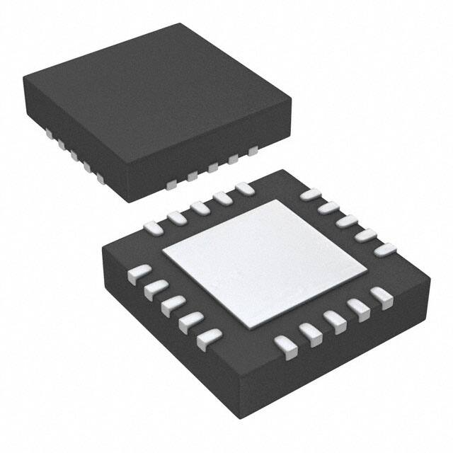
RUK PACKAGE
(TOP VIEW)
VSIM2
•
Level Translator
– VDDIO Range of 1.7 V to 3.3 V
Low-Dropout (LDO) Regulator
– 50-mA LDO Regulator With Enable
– 1.8-V or 2.95-V Selectable Output Voltage
– 2.3-V to 5.5-V Input Voltage Range
– Very Low Dropout: 100 mV (Max) at 50 mA
Control and Communication Through I2C
Interface With Baseband Processor
ESD Protection Exceeds JESD 22
– 2000-V Human-Body Model (A114-B)
– 1000-V Charged-Device Model (C101)
Package
– 20-Pin QFN (3 mm x 3 mm)
SIM2RST
•
Note: The Exposed Thermal Pad must be
connect to Ground.
DESCRIPTION/ORDERING INFORMATION
The TXS02324 is a complete dual-supply standby Smart Identity Module (SIM) card solution for interfacing
wireless baseband processors with two individual SIM subscriber cards to store data for mobile handset
applications. It is a custom device which is used to extend a single SIM/UICC interface to be able to support two
SIMs/UICCs.
The device complies with ISO/IEC Smart-Card Interface requirements as well as GSM and 3G mobile standards.
It includes a high-speed level translator capable of supporting Class-B (2.95 V) and Class-C (1.8 V) interfaces,
two low-dropout (LDO) voltage regulators that have output voltages that are selectable between 2.95-V Class-B
and 1.8-V Class-C interfaces, an integrated "fast-mode" 400 kb/s "slave" I2C control register interface for
configuration purposes, a 32-kHz clock input for internal timing generation.
The voltage-level translator has two supply voltage pins. VDDIO sets the reference for the baseband interface
and can be operated from 1.7 V to 3.3 V. VSIM1 and VSIM2 are programmed to either 1.8 V or 2.95 V, each
supplied by an independent internal LDO regulator. The integrated LDO accepts input battery voltages from 2.3
V to 5.5 V and outputs up to 50 mA to the B-side circuitry and external Class-B or Class-C SIM card.
ORDERING INFORMATION (1)
PACKAGE (2)
TA
–40°C to 85°C
(1)
(2)
QFN – RUK
ORDERABLE PART NUMBER
Tape and reel
TXS02324RUKR
TOP-SIDE MARKING
ZUY
For the most current package and ordering information, see the Package Option Addendum at the end of this document, or see the TI
web site at www.ti.com.
Package drawings, thermal data, and symbolization are available at www.ti.com/packaging.
1
Please be aware that an important notice concerning availability, standard warranty, and use in critical applications of Texas
Instruments semiconductor products and disclaimers thereto appears at the end of this data sheet.
PRODUCTION DATA information is current as of publication date.
Products conform to specifications per the terms of the Texas
Instruments standard warranty. Production processing does not
necessarily include testing of all parameters.
© 2011, Texas Instruments Incorporated
�TXS02324
SCES823 – FEBRUARY 2011
www.ti.com
VBAT
SCK
SDA
2
IC
Control
Logic
LDO
VSIM1
SIM1_RST
SIM_RST
SIM1_CLK
SIM_CLK
Translator
VCC
GND
Reset
VPP
CLK
I/O
NC
NC
SIM1_I/O
SIM_I/O
Baseband
3-V or 1.8-V
SIM Card
V_I/O
VCC
RSTX
LDO
IRQ
VSIM2
SIM2_RST
3-V or 1.8-V
SIM Card
VCC
GND
Reset
VPP
CLK
I/O
NC
NC
SIM2_CLK
Translator
SIM2_I/O
GND
TXS02324
Figure 1. Interfacing With SIM Card
2
Submit Documentation Feedback
© 2011, Texas Instruments Incorporated
Product Folder Link(s): TXS02324
�TXS02324
SCES823 – FEBRUARY 2011
www.ti.com
TERMINAL FUNCTIONS
(1)
NO.
NAME
TYPE (1)
POWER
DOMAIN
1
SIM2RST
O
VSIM2
SIM2 reset
2
VSIM2
O
VSIM2
1.8 V/2.95 V supply voltage to SIM2
3
VBAT
P
VBAT
Battery power supply
4
GND
G
5
VSIM1
O
VSIM1
1.8 V/2.95 V supply voltage to SIM1
6
SIM1RST
O
VSIM1
SIM1 reset
7
SIM1IO
I/O
VSIM1
SIM1 data
8
SIM1CLK
O
VSIM1
SIM1 clock
9
SIMRST
I
VDDIO
UICC/SIM reset from baseband
10
SIMCLK
I
VDDIO
UICC/SIM clock
11
SIMIO
I/O
VDDIO
UICC/SIM data
12
VDDIO
P
VDDIO
1.8-V power supply for device operation and I/O buffers toward baseband
13
SCL
I
VDDIO
I2C clock
14
SDA
I/O
VDDIO
I2C data
15
IRQ
I/O
VDDIO
Interrupt to baseband. This signal is used to set the I2C address.
16
RSTX
I
VDDIO
Active-low reset input from baseband
Do not use. Should not be electrically connected.
DESCRIPTION
Ground
17
DNU
I
VDDIO
18
GND
G
-
GROUND
19
SIM2CLK
O
VSIM2
SIM2 clock
20
SIM2IO
I/O
VSIM2
SIM2 data
G = Ground, I = Input, O = Output, P = Power
Submit Documentation Feedback
© 2011, Texas Instruments Incorporated
Product Folder Link(s): TXS02324
3
�TXS02324
SCES823 – FEBRUARY 2011
www.ti.com
Table 1. Register Overview
REGISTER BITS
B7
B6
B5
B4
B3
B2
B1
B0
COMMAND
BYTE
(HEX)
0
0
0
1
0
0
0
1
00h
Device
hardware
revision
information
R
0001 0001
0
0
0
0
0
0
0
0
01h
Software
revision
information
R
0000 0000
Unused
Unused
Unused
Unused
04h
Status
Register
R
0000 0000
SIM1
Voltage
Select
SIM1
LDO
Enable/
Disable
08h
SIM
Interface
Control
Register
R/W
0000 0000
SIM2 Interface
Status
SIM2 Interface
Status
4
SIM1 Interface
Status
SIM2
Voltage
Select
SIM2
LDO
Enable/
Disable
SIM1 Interface
Status
Submit Documentation Feedback
REGISTER
READ
OR
WRITE
POWER-UP
DEFAULT
© 2011, Texas Instruments Incorporated
Product Folder Link(s): TXS02324
�TXS02324
SCES823 – FEBRUARY 2011
www.ti.com
Table 2. Device Hardware Revision Register (00h)
Device HW Driver Register
HW identification
(1)
Bits(s)
Type (R/W)
7:0
R
Description
This register contains the manufacturer and
device ID (1) (value to be specified by the
manufacturer)
The manufacturer ID part of this data shall remain unchanged when the HW revision ID is updated. The manufacturer ID shall uniquely
identify the manufacturer. The manufacturer ID is encoded on the MSB nibble.
Table 3. Device Software Revision Register (01h)
Device SW Driver Register
SW Driver Version
Bits(s)
7:0
Type (R/W)
R
Description
This register contains information about the
SW driver required for this device. This
information shall only be updated when
changes to the device requires SW
modifications. Initial register value is 00h
Table 4. Status Register (04h)
Bits(s)
Type (R/W)
Unused
Status Register
0
Unused
Unused
Unused
1
Unused
Unused
Unused
2
Unused
Unused
Unused
3
Unused
Unused
SIM1 Interface Status [1:0]
SIM2 Interface Status [1:0]
(1)
5:4
(1)
7:6 (1)
Description
R
Status of SIM1 interface
'00' Powered down with pull-downs activated
'01' Isolated with pull-downs deactivated
'10' Powered with pull downs activated
'11' Active with pull downs deactivated
R
Status of SIM2 interface
'00' Powered down with pull-downs activated
'01' Isolated with pull-downs deactivated
'10' Powered with pull downs activated
'11' Active with pull downs deactivated
The content of bits 5:4 and 7:6 reflects the value written to the state bits in the SIM Interface control register 3:2 and 7:6 respectively
and the setting of the regulator bits in the SIM interface control register 0 and 4 respectively.
Table 5. SIM Interface Control Register (08h) (1) (2)
Status Register
Bit(s)
Type (R/W)
SIM1 Regulator Control
0
R/W
'0' Regulator is off, regulator output is pulled
down
'1' Regulator is powered on, regulator output
pull-down is released
SIM1 Regulator Voltage Selection
1
R/W
'0' 1.8 V
'1' 2.95 V
R/W
Status of SIM1 interface
'00' Powered down state with pull-downs
activated
'01' Isolated state with pull-downs
deactivated
'10' Not allowed
'11' Active state with pull downs deactivated
R/W
'0' Regulator is off, regulator output is pulled
down
'1' Regulator is powered on, regulator output
pull-down is released
SIM1 Interface State [1:0]
SIM2 Regulator Control
(1)
(2)
3:2
4
Description
Reset value: 00h
The state '10', on bits 3:2 and 7:6, is not prevented by HW but shall never be set by SW. State '10' means that the interface is powered
with the pull-downs active, this state correspond to state '00' with the regulator being switched on. Setting the state to '10' does not have
any impact on the corresponding regulator bit setting. The regulator control bits do not impact the state bits in this register. The regulator
control bits however do impact the status bits in the status register.
Submit Documentation Feedback
© 2011, Texas Instruments Incorporated
Product Folder Link(s): TXS02324
5
�TXS02324
SCES823 – FEBRUARY 2011
www.ti.com
Table 5. SIM Interface Control Register (08h)(1)(2) (continued)
Status Register
SIM2 Regulator Voltage
SIM2 Interface State [1:0]
6
Bit(s)
Type (R/W)
5
R/W
'0' 1.8 V
'1' 2.95 V
R/W
Status of SIM2 interface
'00' Powered down state with pull-downs
activated
'01' Isolated state with pull-downs
deactivated
'10' Not allowed
'11' Active state with pull downs deactivated
7:6
Submit Documentation Feedback
Description
© 2011, Texas Instruments Incorporated
Product Folder Link(s): TXS02324
�TXS02324
SCES823 – FEBRUARY 2011
www.ti.com
BASIC DEVICE OPERATION
The TXS02324 is controlled through a standard I2C interface reference to VDDIO. It is connected between the
two SIM card slots and the SIM/UICC interface of the baseband. The device uses VBAT and VDDIO as supply
voltages. The supply voltage for each SIM card is generated by an on-chip low drop out regulator. The interface
between the baseband and the TXS02324 is reference to VDDIO while the interface between the TXS02324 and
the SIM card is referenced to the LDO output of either VSIM1 or VSIM2 depending on which slot is being
selected. The VDDIO on the baseband side normally does not exceed 1.8V, thus voltage level shifting is needed
to support a 3V SIM/UICC interface (Class B).
The TXS02324 has two basic states, the reset and operation state. The baseband utilizes information in the
status registers to determine how to manipulate the control registers to properly switch between two SIM cards.
These fundamental sequences are outlined below and are to help the user to successfully incorporate this device
into the system.
DEVICE ADDRESS
The address of the device is shown below:
Slave Address
0
1
1
1
1
0
IRQ
R/W
Address Reference
IRQ@ Reset
R/W
Slave Address
0
0 (W)
120 (decimal), 78(h)
0
1 (R)
121 (decimal), 79(h)
1
0 (W)
122 (decimal), 7A(h)
1
1 (R)
123 (decimal), 7B(h)
RESET STATE
In the reset state the device settings are brought back to their default values and any SIM card that has been
active is deactivated. After reset, neither of the UICC/SIM interfaces is selected. The active pull-downs at the
UICC/SIM interface are automatically activated. To ensure the system powers up in an operational state, device
uses an internal 32 KHz clock for internal timing generation.
• Power up the TXS02324 by asserting VBAT to enter the operation state
• I2C Interface becomes active with the VDDIO supply
RESET summary:
• Any pending interrupts are cleared
• I2C registers are in the default state
• Both on chip regulators are set to 1.8V and disabled
• All SIM1 and SIM2 signals are pulled to GND
Submit Documentation Feedback
© 2011, Texas Instruments Incorporated
Product Folder Link(s): TXS02324
7
�TXS02324
SCES823 – FEBRUARY 2011
www.ti.com
SETTING UP THE SIM INTERFACE
The TXS02324 supports both Class C (1.8V) or Class B (2.95V) SIM cards. In order to support these cards
types, the interface on the SIM side needs to be properly setup. After power up, the system should default to
SIM1 card. The following sequence outlines a rudimentary sequence of preparing the SIM1 card interface:
• Configure the SIM1 regulator to 1.8V by asserting B1 = 0 in the SIM Interface Control Register (08h). The
system by default should start in 1.8V mode.
• The baseband SIM interface is set to a LOW state.
• Disable the SIM1 interface by asserting B2 = 0 and B3 = 0 in the SIM Interface Control Register.
• Disable the SIM2 interface by asserting B6 = 0 and B7 = 0 in the SIM Interface Control Register.
• VSIM1 voltage regulator should now be activated by asserting B0 = 1 in the SIM Interface Control Register.
• Enable the SIM1 interface by asserting B2 = 1 and B3 = 1 in the SIM Interface Control Register.
• The SIM1 interface (VSIM1, SIM1CLK, SIM1I/O) is now active. The TXS02324 relies on the baseband to
perform the power up sequencing of the SIM card. If there is lack of communication between the baseband
and the SIM card, the SIM1 interface must be powered-down and then powered up again through the
regulator by configuring it to 2.95V by asserting B1 = 1 in the SIM Interface Control Register.
SWITCHING BETWEEN SIM CARDS
The following sequence outlines a rudimentary sequence of switching between the SIM1 card and SIM2 card:
• Put the SIM1 card interface into “clock stop” mode then assert B2 = 1 and B3 = 0 in the SIM Interface Control
Register (08h). This will latch the state of the SIM1 interface (SIM1CLK, SIM1I/O, SIM1RST).
• There can be two scenarios when switching to SIM2 card:
– SIM2 may be in the power off mode, B6 = 0 and B7 = 0 in the Status Register (04h). If SIM2 is in power
off mode, the SIM/UICC interface will need to be set to the power off state. In this case the baseband will
most likely need to go through a power up sequence iteration
– SIM2 may already be in the “clock stop” mode, B6 = 1 and B7 = 0 in the Status Register (04h). If SIM2 is
in “clock stop” mode, the interface between the baseband and the device is set to the clock stop mode
levels that correspond to the SIM2 card interface.
• After determining whether the SIM2 card is either in power off mode or clock stop mode, the SIM2 card
interface is then activated by asserting B6 = 1 and B7 = 1 in the SIM Interface Control Register (08h) and the
negotiation between the baseband and card can continue.
• Switching from SIM2 to SIM1 done in the same manner.
8
Submit Documentation Feedback
© 2011, Texas Instruments Incorporated
Product Folder Link(s): TXS02324
�TXS02324
SCES823 – FEBRUARY 2011
www.ti.com
ABSOLUTE MAXIMUM RATINGS
over operating free-air temperature range (unless otherwise noted)
Level Translator (1)
VDDIO
Supply voltage range
VI
Input voltage range
MIN
MAX
UNIT
–0.3
4.0
V
V_I/O-port
–0.5
4.6
VSIMx-port
–0.5
4.6
Control inputs
–0.5
4.6
V_I/O-port
–0.5
4.6
VSIMx-port
–0.5
4.6
V_I/O-port
–0.5
4.6
VSIMx-port
–0.5
4.6
V
VO
Voltage range applied to any output in the high-impedance or
power-off state
VO
Voltage range applied to any output in the high or low state
IIK
Input clamp current
VI < 0
–50
mA
IOK
Output clamp current
VO < 0
–50
mA
IO
Continuous output current
±50
mA
±100
mA
150
°C
Continuous current through VCCA or GND
Tstg
(1)
–65
Storage temperature range
V
V
Stresses beyond those listed under "absolute maximum ratings" may cause permanent damage to the device. These are stress ratings
only, and functional operation of the device at these or any other conditions beyond those indicated under "recommended operating
conditions" is not implied. Exposure to absolute-maximum-rated conditions for extended periods may affect device reliability.
LDO (1)
MIN
MAX
UNIT
VIN
Input voltage range
–0.3
6
V
VOUT
Output voltage range
–0.3
6
V
TJ
Junction temperature range
–55
150
°C
Tstg
Storage temperature range
–55
150
°C
2
kV
1000
V
ESD rating
(1)
Human-Body Model (HBM)
Charged-Device Model (CDM)
Stresses beyond those listed under "absolute maximum ratings" may cause permanent damage to the device. These are stress ratings
only, and functional operation of the device at these or any other conditions beyond those indicated under "recommended operating
conditions" is not implied. Exposure to absolute-maximum-rated conditions for extended periods may affect device reliability.
Submit Documentation Feedback
© 2011, Texas Instruments Incorporated
Product Folder Link(s): TXS02324
9
�TXS02324
SCES823 – FEBRUARY 2011
www.ti.com
THERMAL IMPEDANCE RATINGS
UNIT
Package thermal impedance (1)
θJA
(1)
RUK package
94.1
°C/W
The package thermal impedance is calculated in accordance with JESD 51-7.
RECOMMENDED OPERATING CONDITIONS (1)
Level Translator
Description
VDDIO
Supply voltage
VIH
High-level input voltage
VIL
Low-level input voltage
Δt/Δv
Input transition rise or fall rate
TA
Operating free-air temperature
(1)
10
Applies to pins: RSTX, SCL,
SDA, IRQ, SIMRST, SIMCLK,
SIMIO
MIN
MAX
UNIT
1.7
3.3
V
VDDIO × 0.7
1.9
V
0
VDDIO × 0.3
V
5
ns/V
85
°C
–40
All unused data inputs of the device must be held at VCCI or GND to ensure proper device operation. Refer to the TI application report,
Implications of Slow or Floating CMOS Inputs, literature number SCBA004.
Submit Documentation Feedback
© 2011, Texas Instruments Incorporated
Product Folder Link(s): TXS02324
�TXS02324
SCES823 – FEBRUARY 2011
www.ti.com
ELECTRICAL CHARACTERISTICS
Level Translator
over recommended operating free-air temperature range (unless otherwise noted)
PARAMETER
SIM1RST
SIM1CLK
SIM1IO
SIM2RST
VOH
SIM2CLK
VOL
Ci
VSIM1
VSIM2
IOH = –100 µA
Push-Pull
TYP (
1)
MAX
VSIM1 × 0.8
VSIM1 × 0.8
1.8 V / 2.95
1.7 V to
V
3.3 V
(Supplied
by LDO)
1.8 V / 2.95
V
(Supplied by
LDO)
VSIM2 × 0.8
V
VSIM2 × 0.8
VSIM2 × 0.8
SIMIO
IOH = –10 µA
Open-Drain
VDDIO × 0.8
SIM1RST
IOL = 1 mA
Push-Pull
VSIM1 × 0.2
SIM1CLK
IOL = 1 mA
Push-Pull
VSIM1 × 0.2
SIM1IO
IOL = 1 mA
Open-Drain
0.3
1.8 V / 2.95
1.7 V to
V
3.3 V
(Supplied
by LDO)
1.8 V / 2.95
V
(Supplied by
LDO)
SIM2RST
IOL = 1 mA
Push-Pull
SIM2CLK
IOL = 1 mA
Push-Pull
SIM2IO
IOL = 1 mA
Open-Drain
0.3
SIMIO
IOL = 1 mA
Open-Drain
0.3
VSIM2 × 0.2
V
VSIM2 × 0.2
VI = OE
1.7 V to
3.3 V
1.8 V / 2.95
V
(Supplied
by LDO)
1.8 V / 2.95
V
(Supplied by
LDO)
±1
µA
VI = VCCI
IO = 0
1.7 V to
3.3 V
1.8 V / 2.95
V
(Supplied
by LDO)
1.8 V / 2.95
V
(Supplied by
LDO)
±5
µA
SIM_I/O
port
7
SIMx port
4
Control
inputs
UNIT
VSIM1 × 0.8
IOH = –100 µA
Push-Pull
IOH = –10 µA
Open-Drain
MIN
IOH = –10 µA
Open-Drain
ICC I/O
Cio
VDDIO
SIM2IO
Control
inputs
II
TEST CONDITIONS
VI = V_I/O or GND
3
pF
pF
Clock input
(1)
All typical values are at TA = 25°C.
Submit Documentation Feedback
© 2011, Texas Instruments Incorporated
Product Folder Link(s): TXS02324
11
�TXS02324
SCES823 – FEBRUARY 2011
www.ti.com
ELECTRICAL CHARACTERISTICS
LDO (Control Input Logic = High)
over operating free-air temperature range (unless otherwise noted)
PARAMETER
VBAT
Input voltage
VOUT
Output voltage
VDO
Dropout voltage
TEST CONDITIONS
TYP (1)
2.3
MAX
UNIT
5.5
V
Class-B Mode
2.82
2.95
3.18
Class-C Mode
1.65
1.8
1.95
IOUT = 50 mA
100
IOUT = 0 mA
35
IOUT = 50 mA
150
IGND
Ground-pin current
ISHDN
Shutdown current (IGND)
VENx ≤ 0.4 V, (VSIMx + VDO) ≤ VBAT ≤ 5.5
V,
TJ = 85°C
IOUT(SC)
Short-circuit current
RL = 0 Ω
COUT
Output Capacitor
f = 1 kHz
50
PSRR
Power-supply rejection ratio
f = 10 kHz
40
TSTR
Start-up time
VSIMx = 1.8 V or 3 V, IOUT = 10 mA,
COUT = 1 µF
TJ
Operating junction
temperature
V
mV
µA
3
µA
400
mA
µF
1
VBAT = 3.25 V,
VSIMx = 1.8 V or 3 V,
COUT = 1 µF, IOUT = 50 mA
(1)
MIN
dB
50
–40
85
µS
°C
All typical values are at TA = 25°C.
GENERAL ELECTRICAL CHARACTERISTICS
over operating free-air temperature range (unless otherwise noted)
PARAMETER
Hyst
Internal hysteresis of comparator
RSIMPU
SIM I/O pull-up
RSIMxPU
SIMx I/O pull-up
RSIMPD
SIMx I/O pull-down
12
TEST CONDITIONS
MIN
TYP
20
kΩ
7.5
Class C
4.5
Submit Documentation Feedback
UNIT
mV
Class B
Active pull-downs are connected to
the VSIM1/2 regulator output to the
SIM1/2 CLK, SIM1/2 RST, SIM1/2
I/O when the respective regulator is
disabled
MAX
±50
2
kΩ
kΩ
© 2011, Texas Instruments Incorporated
Product Folder Link(s): TXS02324
�TXS02324
SCES823 – FEBRUARY 2011
www.ti.com
SWITCHING CHARACTERISTICS
VSIMx = 1.8 V or 2.95 V Supplied by Internal LDO, VBAT = 2.3V to 5.5V
over recommended operating free-air temperature range (unless otherwise noted)
TEST
CONDITIONS
PARAMETER
SIMIO
trA
Baseband side to SIM side
trA
Baseband side to SIM side
V_I/O = 1.7 V to 3.3 V
TYP
UNIT
Open Drain
210
ns
SIMRST
Push Pull
4.3
ns
SIMCLK
Push Pull
4
ns
SIMxIO
Open Drain
16
ns
SIMRST
Push Pull
4
ns
SIMxCLK
Push Pull
5
ns
trB
SIM side to Baseband side
SIMxIO
Open Drain
210
ns
trB
SIM side to Baseband side
SIMxIO
Open Drain
6
ns
fmax
SIMxCLK
Push Pull
5
MHz
SIMCLK to SIMxCLK
Push Pull
8
ns
SIMRST to SIMxRST
Push Pull
8
ns
tPLH
tPHL
SIMIO to SIMxIO
Open Drain
260
ns
SIMxIO to SIMIO
Open Drain
260
ns
SIMCLK to SIMxCLK
Push Pull
7
ns
SIMRST to SIMxRST
Push Pull
7
ns
SIMIO to SIMxIO
Open Drain
23
ns
SIMxIO to SIMIO
Open Drain
23
ns
Submit Documentation Feedback
© 2011, Texas Instruments Incorporated
Product Folder Link(s): TXS02324
13
�TXS02324
SCES823 – FEBRUARY 2011
www.ti.com
OPERATING CHARACTERISTICS
TA = 25°C, VSIMx = 1.8 V for Class C, VSIMx = 2.95 V for Class B
PARAMETER
Cpd
(1)
14
(1)
Class B
Class C
TEST
CONDITIONS
CL = 0,
f = 5 MHz,
tr = tf = 1 ns
TYP
UNIT
11
9.5
pF
Power dissipation capacitance per transceiver
Submit Documentation Feedback
© 2011, Texas Instruments Incorporated
Product Folder Link(s): TXS02324
�TXS02324
SCES823 – FEBRUARY 2011
www.ti.com
APPLICATION INFORMATION
The LDO’s included on the TXS02324 achieve ultra-wide bandwidth and high loop gain, resulting in extremely
high PSRR at very low headroom (VBAT – VSIM1/2). The TXS02324 provides fixed regulation at 1.8V or 2.95V.
Low noise, enable (through I2C control), low ground pin current make it ideal for portable applications. The device
offers sub-bandgap output voltages, current limit and thermal protection, and is fully specified from –40°C to
+85°C.
VSIM1
VDDIO
TXS02324
VBAT
0.1μF
GND
0.1μF
VSIM2
0.1μF
0.1μF
Figure 2. Typical Application circuit for TXS02324
Input and Output Capacitor Requirements
It is good analog design practice to connect a 1.0 μF low equivalent series resistance (ESR) capacitor across the
input supply (VBAT) near the regulator. Also, a 0.1uF is required for the logic core supply (VDDIO).
This capacitor will counteract reactive input sources and improve transient response, noise rejection, and ripple
rejection. A higher-value capacitor may be necessary if large, fast rise-time load transients are anticipated or if
the device is located several inches from the power source. The LDO’s are designed to be stable with standard
ceramic capacitors of values 1.0 μF or larger. X5R- and X7R-type capacitors are best because they have
minimal variation in value and ESR over temperature. Maximum ESR should be < 1.0 Ω.
Output Noise
In most LDO’s, the bandgap is the dominant noise source. To improve ac performance such as PSRR, output
noise, and transient response, it is recommended that the board be designed with separate ground planes for VIN
and VOUT, with each ground plane connected only at the GND pin of the device. In addition, the ground
connection for the bypass capacitor should connect directly to the GND pin of the device.
Internal Current Limit
The TXS02324 internal current limit helps protect the regulator during fault conditions. During current limit, the
output sources a fixed amount of current that is largely independent of output voltage. For reliable operation, the
device should not be operated in a current limit state for extended periods of time.
The PMOS pass element in the TXS02324 has a built-in body diode that conducts current when the voltage at
VSIM1/2 exceeds the voltage at VBAT. This current is not limited, so if extended reverse voltage operation is
anticipated, external limiting may be appropriate.
Dropout Voltage
The TXS02324 uses a PMOS pass transistor to achieve low dropout. When (VBAT – VSIM1/2) is less than the
dropout voltage (VDO), the PMOS pass device is in its linear region of operation and the input-to-output
resistance is the RDS(ON) of the PMOS pass element. VDO will approximately scale with output current because
the PMOS device behaves like a resistor in dropout.
Startup
The TXS02324 uses a quick-start circuit which allows the combination of very low output noise and fast start-up
times. Note that for fastest startup, VBATT should be applied first, and then enabled by asserting the I2C register.
Submit Documentation Feedback
© 2011, Texas Instruments Incorporated
Product Folder Link(s): TXS02324
15
�TXS02324
SCES823 – FEBRUARY 2011
www.ti.com
Transient Response
As with any regulator, increasing the size of the output capacitor reduces over/undershoot magnitude but
increases duration of the transient response.
Minimum Load
The TXS02324 is stable and well-behaved with no output load. Traditional PMOS LDO regulators suffer from
lower loop gain at very light output loads. The TXS02324 employs an innovative low-current mode circuit to
increase loop gain under very light or no-load conditions, resulting in improved output voltage regulation
performance down to zero output current.
THERMAL INFORMATION
Thermal Protection
Thermal protection disables the output when the junction temperature rises to approximately +160°C, allowing
the device to cool. When the junction temperature cools to approximately +140°C the output circuitry is again
enabled. Depending on power dissipation, thermal resistance, and ambient temperature, the thermal protection
circuit may cycle on and off. This cycling limits the dissipation of the regulator, protecting it from damage
because of overheating.
Any tendency to activate the thermal protection circuit indicates excessive power dissipation or an inadequate
heat sink. For reliable operation, junction temperature should be limited to +85°C maximum. To estimate the
margin of safety in a complete design (including heat sink), increase the ambient temperature until the thermal
protection is triggered; use worst-case loads and signal conditions. For good reliability, thermal protection should
trigger at least +35°C above the maximum expected ambient condition of your particular application. This
configuration produces a worst-case junction temperature of +85°C at the highest expected ambient temperature
and worst-case load.
The internal protection circuitry of the TXS02324 has been designed to protect against overload conditions. It
was not intended to replace proper heat sinking. Continuously running the TXS02324 into thermal shutdown will
degrade device reliability.
TYPICAL CHARACTERISTICS
110
-80
90
-70
-60
-50
2.95 V Vsim
-40
-30
-20
80
85°C Vsim
70
60
50
40
-40°C Vsim
30
20
-10
0
100
25°C Vsim
10
1000
10000
100000
f - Frequency - Hz
Figure 3. PSRR
16
100
1.8 V Vsim
VDO - Dropout Voltage - mV
PSRR - Power Supply Rejection Ratio - dB
-90
1000000
0
0
5
10
15 20 25 30 35 40
IOUT - Output Current - mA
45
50
Figure 4. Dropout Voltage vs Output Current
Submit Documentation Feedback
© 2011, Texas Instruments Incorporated
Product Folder Link(s): TXS02324
�TXS02324
SCES823 – FEBRUARY 2011
www.ti.com
0
IO = 50 mA
-0.2
-0.4
-100 mA, Vsim
DVOUT - Output Voltage - %
DVOUT - Output Voltage - %
TYPICAL CHARACTERISTICS (continued)
1
0.8
0.6
0.4
0.2
0
-0.2
-0.4
-0.6
-0.8
-1
-1.2
-1.4
-1.6
-1.8
-2
-2.2
-2.4
-40 -30 -20 -10
-50 mA, Vsim
-0.6
-40°C Vsim
85°C Vsim
-0.8
-1
-1.2
-1.4
25°C Vsim
-1.6
-1.8
0
-2
0
10 20 30 40 50 60 70 80
5
10
TA - Temperature - °C
Figure 5. Output Voltage vs Temperature, Class-B/C
45
50
Figure 6. Load Regulation, Iout = 50 mA, Class-C
0.2
0
0
-0.2
-40°C Vsim
IO = 50 mA
-0.4
-0.2
DVOUT - Output Voltage - %
DVOUT - Output Voltage - %
15 20 25 30 35 40
IOUT - Output Current - mA
-0.4
-0.6
25°C Vsim
-0.8
85°C Vsim
-1
-1.2
-1.4
-1.6
-0.6
-0.8
-40°C Vsim
-1
-1.2
25°C Vsim
-1.4
-1.6
85°C Vsim
-1.8
-2
IO = 50 mA
-1.8
-2
0
5
10
15
20 25 30 35 40
IOUT - Output Current - mA
45
Figure 7. Load Regulation, Iout = 50 mA, Class-B
-2.2
50
-2.4
2.7
3.1
3.5
3.9
4.3
VBAT - V
4.7
5.1
5.5
Figure 8. Line Regulation, Iout = 50 mA, Class-C
Submit Documentation Feedback
© 2011, Texas Instruments Incorporated
Product Folder Link(s): TXS02324
17
�TXS02324
SCES823 – FEBRUARY 2011
www.ti.com
TYPICAL CHARACTERISTICS (continued)
330
0
300
DVOUT - Output Voltage - %
-0.4
-40°C Vsim
270
IOUT(SC) - Output Current - mA
-0.2
IO = 50 mA
-0.6
-0.8
25°C Vsim
-1
85°C Vsim
-1.2
-1.4
-1.6
-1.8
240
210
25°C Vsim
150
120
90
60
-2.2
30
Figure 9. Line Regulation, Iout = 50 mA, Class-B
85°C Vsim
180
-2
-2.4
3.1 3.3 3.5 3.7 3.9 4.1 4.3 4.5 4.7 4.9 5.1 5.3 5.5
VBAT - V
-40°C Vsim
0
2.7
3.1
3.5
3.9
4.3
VBAT - V
4.7
5.1
5.5
Figure 10. Current Limit vs Input Voltage, Class-B/C
150
-50 mA, Vsim
IGND - Ground Current - mA
120
90
60
30
-100 mA, Vsim
0
-40 -30 -20 -10
20 30 40 50 60 70 80
TA - ºC
Figure 11. Ground Current vs Temperature, Class-C
18
0 10
Submit Documentation Feedback
© 2011, Texas Instruments Incorporated
Product Folder Link(s): TXS02324
�PACKAGE OPTION ADDENDUM
www.ti.com
10-Dec-2020
PACKAGING INFORMATION
Orderable Device
Status
(1)
Package Type Package Pins Package
Drawing
Qty
Eco Plan
(2)
Lead finish/
Ball material
MSL Peak Temp
Op Temp (°C)
Device Marking
(3)
(4/5)
(6)
TXS02324RUKR
ACTIVE
WQFN
RUK
20
3000
RoHS & Green
NIPDAU
Level-2-260C-1 YEAR
-40 to 85
ZUY
(1)
The marketing status values are defined as follows:
ACTIVE: Product device recommended for new designs.
LIFEBUY: TI has announced that the device will be discontinued, and a lifetime-buy period is in effect.
NRND: Not recommended for new designs. Device is in production to support existing customers, but TI does not recommend using this part in a new design.
PREVIEW: Device has been announced but is not in production. Samples may or may not be available.
OBSOLETE: TI has discontinued the production of the device.
(2)
RoHS: TI defines "RoHS" to mean semiconductor products that are compliant with the current EU RoHS requirements for all 10 RoHS substances, including the requirement that RoHS substance
do not exceed 0.1% by weight in homogeneous materials. Where designed to be soldered at high temperatures, "RoHS" products are suitable for use in specified lead-free processes. TI may
reference these types of products as "Pb-Free".
RoHS Exempt: TI defines "RoHS Exempt" to mean products that contain lead but are compliant with EU RoHS pursuant to a specific EU RoHS exemption.
Green: TI defines "Green" to mean the content of Chlorine (Cl) and Bromine (Br) based flame retardants meet JS709B low halogen requirements of


 工商网监
湘ICP备2023018690号
工商网监
湘ICP备2023018690号
