Product
Folder
Order
Now
Technical
Documents
Support &
Community
Tools &
Software
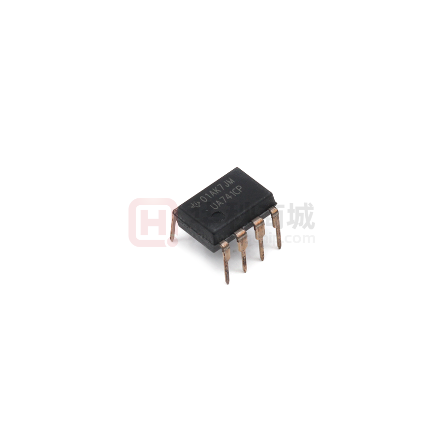
uA741
SLOS094G – NOVEMBER 1970 – REVISED JANUARY 2018
µA741 General-Purpose Operational Amplifiers
1 Features
3 Description
•
•
•
The µA741 device is a general-purpose operational
amplifier featuring offset-voltage null capability.
1
•
•
Short-Circuit Protection
Offset-Voltage Null Capability
Large Common-Mode and Differential Voltage
Ranges
No Frequency Compensation Required
No Latch-Up
The high common-mode input voltage range and the
absence of latch-up make the amplifier ideal for
voltage-follower
applications.
The
device
is
short-circuit protected and the internal frequency
compensation ensures stability without external
components. A low-value potentiometer may be
connected between the offset null inputs to null out
the offset voltage as shown in Figure 12.
2 Applications
•
•
DVD Recorders and Players
Pro Audio Mixers
The µA741C device is characterized for operation
from 0°C to 70°C.
Device Information(1)
PART NUMBER
PACKAGE
BODY SIZE (NOM)
µA741CD
SOIC (8)
4.90 mm × 3.91 mm
µA741CP
PDIP (8)
9.81 mm × 6.35 mm
µA741CPS
SO (8)
6.20 mm × 5.30 mm
(1) For all available packages, see the orderable addendum at
the end of the data sheet.
Simplified Schematic
OFFSET N1
IN +
+
IN –
–
OUT
OFFSET N2
1
An IMPORTANT NOTICE at the end of this data sheet addresses availability, warranty, changes, use in safety-critical applications,
intellectual property matters and other important disclaimers. PRODUCTION DATA.
�uA741
SLOS094G – NOVEMBER 1970 – REVISED JANUARY 2018
www.ti.com
Table of Contents
1
2
3
4
5
6
7
Features ..................................................................
Applications ...........................................................
Description .............................................................
Revision History.....................................................
Pin Configurations and Functions .......................
Specifications.........................................................
1
1
1
2
4
5
6.1
6.2
6.3
6.4
6.5
6.6
6.7
6.8
5
5
5
6
7
7
7
8
Absolute Maximum Ratings ......................................
Recommended Operating Conditions.......................
Thermal Information ..................................................
Electrical Characteristics: μA741C............................
Electrical Characteristics: μA741Y ............................
Switching Characteristics: μA741C ...........................
Switching Characteristics: μA741Y ...........................
Typical Characteristics ..............................................
Detailed Description ............................................ 10
7.1 Overview ................................................................. 10
7.2 Functional Block Diagram ....................................... 10
7.3 Feature Description................................................. 10
7.4 Device Functional Modes........................................ 11
7.5 µA741Y Chip Information........................................ 11
8
Application and Implementation ........................ 12
8.1 Application Information............................................ 12
8.2 Typical Application .................................................. 12
9 Power Supply Recommendations...................... 14
10 Layout................................................................... 14
10.1 Layout Guidelines ................................................. 14
10.2 Layout Example .................................................... 14
11 Device and Documentation Support ................. 16
11.1
11.2
11.3
11.4
Receiving Notification of Documentation Updates
Trademarks ...........................................................
Electrostatic Discharge Caution ............................
Glossary ................................................................
16
16
16
16
12 Mechanical, Packaging, and Orderable
Information ........................................................... 16
4 Revision History
Changes from Revision F (May 2017) to Revision G
•
Page
Changed supply voltage unit from "°C" to "V" in Absolute Maximum Ratings table ............................................................. 5
Changes from Revision E (January 2015) to Revision F
Page
•
Updated data sheet text to the latest documentation and translation standards .................................................................. 1
•
Deleted text regarding µA741M device (obsolete package) from Description section........................................................... 1
•
Added µA741CD, µA741CP, and µA741CPS devices to Device Information table .............................................................. 1
•
Deleted µA741x device from Device Information table ......................................................................................................... 1
•
Updated pinout diagrams and Pin Functions tables in the Pin Configurations and Functions section .................................. 4
•
Deleted µA741M pinout drawings information from Pin Configurations and Functions section ............................................ 4
•
Deleted Electrical Characteristics: µA741M table from Specifications section ...................................................................... 5
•
Added operating junction temperature (TJ) and values to Absolute Maximum Ratings table ............................................... 5
•
Deleted text regarding µA741M from Absolute Maximum Ratings table .............................................................................. 5
•
Deleted text regarding µA741M device from Recommended Operating Conditions table .................................................... 5
•
Deleted Dissipation Ratings table .......................................................................................................................................... 5
•
Added Thermal Information table and values ........................................................................................................................ 5
•
Deleted µA741M in Switching Characteristics table .............................................................................................................. 7
•
Correct typo in Figure 1 ......................................................................................................................................................... 8
•
Deleted text regarding µA741M device from Detailed Description section .......................................................................... 10
•
Updated text in Overview section ........................................................................................................................................ 10
•
Added 2017 copyright to Functional Block Diagram ........................................................................................................... 10
•
Added caption to Figure 11 in Device Functional Modes section ........................................................................................ 11
•
Changed pins 1 and 5 from "NC" to "Offset N1" and "Offset N2" in Figure 18 .................................................................... 15
2
Submit Documentation Feedback
Copyright © 1970–2018, Texas Instruments Incorporated
Product Folder Links: uA741
�uA741
www.ti.com
SLOS094G – NOVEMBER 1970 – REVISED JANUARY 2018
Changes from Revision D (February 2014) to Revision E
Page
•
Added Applications, Device Information table, Pin Functions table, ESD Ratings table, Thermal Information table,
Feature Description section, Device Functional Modes, Application and Implementation section, Power Supply
Recommendations section, Layout section, Device and Documentation Support section, and Mechanical,
Packaging, and Orderable Information section. ..................................................................................................................... 1
•
Moved Typical Characteristics into Specifications section. ................................................................................................... 8
Changes from Revision C (January 2014) to Revision D
•
Page
Fixed Typical Characteristics graphs to remove extra lines. ................................................................................................. 8
Changes from Revision B (September 2000) to Revision C
Page
•
Updated document to new TI data sheet format - no specification changes. ........................................................................ 1
•
Deleted Ordering Information table. ....................................................................................................................................... 1
Submit Documentation Feedback
Copyright © 1970–2018, Texas Instruments Incorporated
Product Folder Links: uA741
3
�uA741
SLOS094G – NOVEMBER 1970 – REVISED JANUARY 2018
www.ti.com
5 Pin Configurations and Functions
uA741C D, P, or PS Package
8-Pin SOIC, PDIP, SO
Top View
OFFSET N1
1
8
NC
IN±
2
7
VCC+
IN+
3
6
OUT
VCC±
4
5
OFFSET N2
Not to scale
NC- no internal connection
Pin Functions
PIN
NAME
NO.
I/O
DESCRIPTION
IN+
3
I
Noninverting input
IN–
2
I
Inverting input
NC
8
—
OFFSET N1
1
I
External input offset voltage adjustment
OFFSET N2
5
I
External input offset voltage adjustment
OUT
6
O
Output
VCC+
7
—
Positive supply
VCC–
4
—
Negative supply
4
No internal connection
Submit Documentation Feedback
Copyright © 1970–2018, Texas Instruments Incorporated
Product Folder Links: uA741
�uA741
www.ti.com
SLOS094G – NOVEMBER 1970 – REVISED JANUARY 2018
6 Specifications
6.1 Absolute Maximum Ratings
over virtual junction temperature range (unless otherwise noted) (1)
MIN
MAX
Supply voltage, VCC (2)
µA741C
–18
18
V
Differential input voltage, VID (3)
µA741C
–15
15
V
µA741C
–15
15
V
µA741C
–15
15
V
Input voltage, VI (any input)
(2) (4)
Voltage between offset null (either OFFSET N1 or
OFFSET N2) and VCC–
Duration of output short circuit
(5)
UNIT
Unlimited
Continuous total power dissipation
See Thermal Information
Case temperature for 60 seconds
µA741C
N/A
N/A
°C
Lead temperature 1.6 mm (1/16 inch) from case for 60 seconds
µA741C
N/A
N/A
°C
Lead temperature 1.6 mm (1/16 inch) from case for 10
seconds
µA741C
260
°C
150
°C
150
°C
D, P, or PS package
Operating junction temperature, TJ
Storage temperature range, Tstg
(1)
(2)
(3)
(4)
(5)
µA741C
–65
Stresses beyond those listed under Absolute Maximum Ratings may cause permanent damage to the device. These are stress ratings
only, and functional operation of the device at these or any other conditions beyond those indicated under Recommended Operating
Conditions is not implied. Exposure to absolute-maximum-rated conditions for extended periods may affect device reliability.
All voltage values, unless otherwise noted, are with respect to the midpoint between VCC+ and VCC–.
Differential voltages are at IN+ with respect to IN –.
The magnitude of the input voltage must never exceed the magnitude of the supply voltage or 15 V, whichever is less.
The output may be shorted to ground or either power supply.
6.2 Recommended Operating Conditions
VCC+
VCC–
TA
Supply voltage
Operating free-air temperature
µA741C
MIN
MAX
5
15
–5
–15
0
70
UNIT
V
°C
6.3 Thermal Information
µA741
THERMAL METRIC (1)
D (SOIC)
P (PDIP)
PS (SO)
8 PINS
8 PINS
8 PINS
129.2
87.4
119.7
°C/W
RθJC(top) Junction-to-case (top) thermal resistance
73.6
89.3
66
°C/W
RθJB
Junction-to-board thermal resistance
72.4
64.4
70
°C/W
ψJT
Junction-to-top characterization parameter
25.9
49.8
27.2
°C/W
ψJB
Junction-to-board characterization parameter
71.7
64.1
69
°C/W
RθJA
(1)
Junction-to-ambient thermal resistance
UNIT
For more information about traditional and new thermal metrics, see the Semiconductor and IC Package Thermal Metrics application
report.
Submit Documentation Feedback
Copyright © 1970–2018, Texas Instruments Incorporated
Product Folder Links: uA741
5
�uA741
SLOS094G – NOVEMBER 1970 – REVISED JANUARY 2018
www.ti.com
6.4 Electrical Characteristics: μA741C
at specified virtual junction temperature, VCC± = ±15 V (unless otherwise noted)
TEST CONDITIONS (1)
PARAMETER
VIO
Input offset voltage
VO = 0
ΔVIO(adj)
Offset voltage adjust range
VO = 0
IIO
Input offset current
VO = 0
IIB
Input bias current
VO = 0
VICR
Common-mode input voltage range
MIN
25°C
25°C
±15
25°C
20
Full range
25°C
80
Full range
RL = 10 kΩ
25°C
±12
RL ≥ 10 kΩ
Full range
±12
RL = 2 kΩ
25°C
±10
±10
VOM
Maximum peak output voltage swing
RL ≥ 2 kΩ
Full range
AVD
Large-signal differential voltage
amplification
RL ≥ 2 kΩ
25°C
20
VO = ±10 V
Full range
15
ri
Input resistance
25°C
ro
Output resistance
VO = 0; see (2)
Ci
Input capacitance
25°C
CMRR
Common-mode rejection ratio
VIC = VICRmin
kSVS
Supply voltage sensitivity (ΔVIO/ΔVCC)
VCC = ±9 V to ±15 V
IOS
Short-circuit output current
25°C
0.3
PD
Total power dissipation
VO = 0; no load
(1)
(2)
6
25°C
25°C
70
Full range
70
25°C
±13
Full range
nA
nA
V
V
200
V/mV
2
MΩ
75
Ω
1.4
pF
90
30
dB
150
150
±25
±40
1.7
2.8
Full range
25°C
mV
±14
Full range
25°C
500
800
±12
UNIT
mV
200
300
±12
VO = 0; no load
6
7.5
Full range
Supply current
MAX
1
Full range
25°C
ICC
TYP
3.3
50
85
100
µV/V
mA
mA
mW
All characteristics are measured under open-loop conditions with zero common-mode input voltage unless otherwise specified.
Full range for the µA741C is 0°C to 70°C.
This typical value applies only at frequencies above a few hundred hertz because of the effects of drift and thermal feedback.
Submit Documentation Feedback
Copyright © 1970–2018, Texas Instruments Incorporated
Product Folder Links: uA741
�uA741
www.ti.com
SLOS094G – NOVEMBER 1970 – REVISED JANUARY 2018
6.5 Electrical Characteristics: μA741Y
at specified virtual junction temperature, VCC± = ±15 V, TA = 25°C (unless otherwise noted) (1)
PARAMETER
TEST CONDITIONS
(2)
TYP
MAX
VIO
Input offset voltage
VO = 0
1
5
ΔVIO(adj)
Offset voltage adjust range
VO = 0
±15
IIO
Input offset current
VO = 0
20
200
nA
IIB
Input bias current
VO = 0
80
500
nA
VICR
Common-mode input voltage range
UNIT
mV
mV
±12
±13
RL = 10 kΩ
±12
±14
RL = 2 kΩ
±10
±13
20
200
0.3
2
MΩ
75
Ω
VOM
Maximum peak output voltage swing
AVD
Large-signal differential voltage amplification
ri
Input resistance
ro
Output resistance
Ci
Input capacitance
CMRR
Common-mode rejection ratio
VIC = VICRmin
kSVS
Supply voltage sensitivity (ΔVIO/ΔVCC)
VCC = ±9 V to ±15 V
IOS
Short-circuit output current
ICC
Supply current
PD
Total power dissipation
(1)
(2)
MIN
RL ≥ 2 kΩ
VO = 0; see (1)
V
V
V/mV
1.4
pF
90
dB
70
30
150
µV/V
±25
±40
mA
VO = 0; no load
1.7
2.8
mA
VO = 0; no load
50
85
mW
This typical value applies only at frequencies above a few hundred hertz because of the effects of drift and thermal feedback.
All characteristics are measured under open-loop conditions with zero common-mode voltage unless otherwise specified.
6.6 Switching Characteristics: μA741C
over operating free-air temperature range, VCC± = ±15 V, TA = 25°C (unless otherwise noted)
PARAMETER
tr
Rise time
Overshoot factor
SR
Slew rate at unity gain
TEST CONDITIONS
MIN
TYP
MAX
UNIT
0.3
VI = 20 mV, RL = 2 kΩ
CL = 100 pF; see Figure 1
µs
5%
VI = 10 V, RL = 2 kΩ
CL = 100 pF; see Figure 1
0.5
V/µs
6.7 Switching Characteristics: μA741Y
over operating free-air temperature range, VCC± = ±15 V, TA = 25°C (unless otherwise noted)
PARAMETER
tr
Rise time
Overshoot factor
SR
Slew rate at unity gain
TEST CONDITIONS
VI = 20 mV, RL = 2 kΩ
CL = 100 pF; see Figure 1
VI = 10 V, RL = 2 kΩ
CL = 100 pF; see Figure 1
MIN
TYP
MAX
0.3
Product Folder Links: uA741
µs
5%
0.5
Submit Documentation Feedback
Copyright © 1970–2018, Texas Instruments Incorporated
UNIT
V/µs
7
�uA741
SLOS094G – NOVEMBER 1970 – REVISED JANUARY 2018
www.ti.com
6.8 Typical Characteristics
Data at high and low temperatures are applicable only within the rated operating free-air temperature ranges of the various
devices.
VI
–
OUT
IN
+
0V
INPUT VOLTAGE
WAVEFORM
CL = 100 pF
RL = 2 kΩ
TEST CIRCUIT
Figure 1. Rise Time, Overshoot, and Slew Rate
100
400
VCC+ = 15 V
VCC – = –15 V
350
I IB – Input Bias Current – nA
I IO – Input Offset Current – nA
90
80
70
60
50
40
30
VCC+ = 15 V
VCC – = –15 V
300
250
200
150
100
20
50
10
0
– 60 – 40 – 20
0
20
40
60
0
– 60 – 40 – 20
80 100 120 140
Figure 2. Input Offset Current vs Free-Air Temperature
± 11
±10
±9
±8
±7
±6
±5
±4
0.1
0.2
0.4
0.7 1
2
4
7
±18
±16
60
80 100 120 140
VCC+ = 15 V
VCC – = –15 V
RL = 10 kΩ
TA = 25°C
±14
±12
±10
±8
±6
±4
±2
0
100
10
RL – Load Resistance – kΩ
1k
10k
100k
1M
f – Frequency – Hz
Figure 4. Maximum Output Voltage vs Load Resistance
8
40
±20
VCC+ = 15 V
VCC – = –15 V
TA = 25°C
VOM – Maximum Peak Output Voltage – V
VOM – Maximum Peak Output Voltage – V
±12
20
Figure 3. Input Bias Current vs Free-Air Temperature
±14
±13
0
TA – Free-Air Temperature – °C
TA – Free-Air Temperature – °C
Figure 5. Maximum Peak Output Voltage vs Frequency
Submit Documentation Feedback
Copyright © 1970–2018, Texas Instruments Incorporated
Product Folder Links: uA741
�uA741
www.ti.com
SLOS094G – NOVEMBER 1970 – REVISED JANUARY 2018
Typical Characteristics (continued)
Data at high and low temperatures are applicable only within the rated operating free-air temperature ranges of the various
devices.
110
VO = ±10 V
RL = 2 kΩ
TA = 25°C
200
VCC+ = 15 V
VCC – = –15 V
VO = ±10 V
RL = 2 kΩ
TA = 25°C
100
AVD – Open-Loop Signal Differential
Voltage Amplification – dB
AVD – Open-Loop Signal Differential
Voltage Amplification – V/mV
400
100
40
20
90
80
70
60
50
40
30
20
10
0
10
0
2
4
6
8
10
12
14
16
18
–10
1
20
10
100
VCC ± – Supply Voltage – V
Figure 6. Open-Loop Signal Differential Voltage
Amplification vs Supply Voltage
1M
100k
10M
Figure 7. Open-Loop Large-Signal Differential Voltage
Amplification vs Frequency
28
100
VCC+ = 15 V
VCC– = –15 V
BS = 10 kΩ
TA = 25°C
90
80
24
20
VO – Output Voltage – mV
CMRR – Common-Mode Rejection Ratio – dB
10k
1k
f – Frequency – Hz
70
60
50
40
30
20
90%
16
12
8
VCC+ = 15 V
VCC– = –15 V
RL = 2 kΩ
CL = 100 pF
TA = 25°C
4
10%
0
10
tr
–4
0
1
100
10k
1M
100M
0
f – Frequency – Hz
0.5
1
1.5
2
2.5
t – Time - µs
Figure 8. Common-Mode Rejection Ratio vs Frequency
Figure 9. Output Voltage vs Elapsed Time
8
VCC+ = 15 V
VCC– = –15 V
RL = 2 kΩ
CL = 100 pF
TA = 25°C
Input and Output Voltage – V
6
4
VO
2
0
VI
–2
–4
–6
–8
0
10
20
30
40
50
60
70
80
90
t – Time – ms
Figure 10. Voltage-Follower Large-Signal Pulse Response
Submit Documentation Feedback
Copyright © 1970–2018, Texas Instruments Incorporated
Product Folder Links: uA741
9
�uA741
SLOS094G – NOVEMBER 1970 – REVISED JANUARY 2018
www.ti.com
7 Detailed Description
7.1 Overview
The μA741 has been a popular operational amplifier for over four decades. Typical open loop gain is 106 dB
while driving a 2000-Ω load. Short circuit tolerance, offset voltage trimming, and unity-gain stability makes the
μA741 useful for many applications.
7.2 Functional Block Diagram
VCC+
IN –
OUT
IN+
OFFSET N1
OFFSET N2
VCC –
Component Count
Transistors
Resistors
Diode
Capacitor
22
11
1
1
Copyright © 2017, Texas Instruments Incorporated
7.3 Feature Description
7.3.1 Offset-Voltage Null Capability
The input offset voltage of operational amplifiers (op amps) arises from unavoidable mismatches in the
differential input stage of the op-amp circuit caused by mismatched transistor pairs, collector currents, currentgain betas (β), collector or emitter resistors and so forth. The input offset pins allow the designer to adjust for
mismatches caused by external circuitry. See Application and Implementation for more details on design
techniques.
10
Submit Documentation Feedback
Copyright © 1970–2018, Texas Instruments Incorporated
Product Folder Links: uA741
�uA741
www.ti.com
SLOS094G – NOVEMBER 1970 – REVISED JANUARY 2018
Feature Description (continued)
7.3.2 Slew Rate
The slew rate is the rate at which an operational amplifier can change an output when there is a change on the
input. The µA741 device has a 0.5-V/μs slew rate. Parameters that vary significantly with operating voltages or
temperature are shown in Typical Characteristics.
7.4 Device Functional Modes
The µA741 device is powered on when the power supply is connected. The device can operate as a singlesupply or dual-supply operational amplifier depending on the application.
7.5 µA741Y Chip Information
When properly assembled, this chip displays characteristics similar to the µA741C device. Thermal compression
or ultrasonic bonding may be used on the doped-aluminum bonding pads. Chips can be mounted with conductive
epoxy or a gold-silicon preform.
BONDING PAD ASSIGNMENTS
(7)
(6)
IN +
IN –
(8)
(3)
(2)
OFFSET N1
(1)
OFFSET N2
(5)
VCC+
(7)
+
(6)
OUT
–
(4)
VCC –
45
(5)
(1)
(4)
CHIP THICKNESS: 15 TYPICAL
BONDING PADS: 4 × 4 MINIMUM
TJmax = 150 °C.
(2)
(3)
TOLERANCES ARE ± 10%.
ALL DIMENSIONS ARE IN MILS.
36
Figure 11. Bonding Pad Assignments
Submit Documentation Feedback
Copyright © 1970–2018, Texas Instruments Incorporated
Product Folder Links: uA741
11
�uA741
SLOS094G – NOVEMBER 1970 – REVISED JANUARY 2018
www.ti.com
8 Application and Implementation
NOTE
Information in the following applications sections is not part of the TI component
specification, and TI does not warrant its accuracy or completeness. TI’s customers are
responsible for determining suitability of components for their purposes. Customers should
validate and test their design implementation to confirm system functionality.
8.1 Application Information
The input offset voltage of operational amplifiers (op amps) arises from unavoidable mismatches in the
differential input stage of the op-amp circuit caused by mismatched transistor pairs, collector currents, currentgain betas (β), collector or emitter resistors and so forth. The input offset pins allow the designer to adjust for
mismatches resulting from external circuitry. These input mismatches can be adjusted by placing resistors or a
potentiometer between the inputs as shown in Figure 12. A potentiometer can fine-tune the circuit during testing
or for applications which require precision offset control. For more information about designing using the inputoffset pins, see Nulling Input Offset Voltage of Operational Amplifiers.
+
IN +
OUT
IN –
OFFSET N2
–
OFFSET N1
10 kΩ
To VCC –
Figure 12. Input Offset Voltage Null Circuit
8.2 Typical Application
The voltage follower configuration of the operational amplifier is used for applications where a weak signal drives
a relatively high current load. This circuit is also called a buffer amplifier or unity-gain amplifier. The inputs of an
operational amplifier have a very high resistance which puts a negligible current load on the voltage source. The
output resistance of the operational amplifier is almost negligible, so the resistance can provide as much current
as necessary to the output load.
10 k
12 V
VOUT
+
VIN
Figure 13. Voltage Follower Schematic
12
Submit Documentation Feedback
Copyright © 1970–2018, Texas Instruments Incorporated
Product Folder Links: uA741
�uA741
www.ti.com
SLOS094G – NOVEMBER 1970 – REVISED JANUARY 2018
Typical Application (continued)
8.2.1 Design Requirements
• Output range from 2 V to 11.5 V
• Input range from 2 V to 11.5 V
• Resistive feedback to negative input
8.2.2 Detailed Design Procedure
8.2.2.1 Output Voltage Swing
The output voltage of an operational amplifier is limited by the internal circuitry to some level below the supply
rails. For this amplifier, the output voltage swing is within ±12 V, which accommodates the input and output
voltage requirements.
8.2.2.2 Supply and Input Voltage
For correct operation of the amplifier, neither input must be higher than the recommended positive supply rail
voltage or lower than the recommended negative supply rail voltage. The selected amplifier must be able to
operate at the supply voltage that accommodates the inputs. Because the input for this application goes up to
11.5 V, the supply voltage must be 12 V. Using a negative voltage on the lower rail rather than ground allows the
amplifier to maintain linearity for inputs below 2 V.
8.2.3 Application Curves for Output Characteristics
12
0.045
0.040
10
0.035
0.030
0.025
IIO (mA)
VOUT (V)
8
6
0.020
0.015
4
0.010
0.005
2
0.000
0
±0.005
0
2
4
6
8
10
VIN (V)
12
0
2
4
6
8
10
VIN (V)
C001
Figure 14. Output Voltage vs Input Voltage
12
C002
Figure 15. Current Drawn Input of Voltage Follower (IIO)
vs Input Voltage
0.45
0.40
0.35
ICC (mA)
0.30
0.25
0.20
0.15
0.10
0.05
0.00
0
2
4
6
8
10
VIN (V)
12
C003
Figure 16. Current Drawn from Supply (ICC)
vs Input Voltage
Submit Documentation Feedback
Copyright © 1970–2018, Texas Instruments Incorporated
Product Folder Links: uA741
13
�uA741
SLOS094G – NOVEMBER 1970 – REVISED JANUARY 2018
www.ti.com
9 Power Supply Recommendations
The μA741 device is specified for operation from ±5 to ±15 V; many specifications apply from 0°C to 70°C.
Typical Characteristics presents parameters that can exhibit significant variance with regard to operating voltage
or temperature.
Place 0.1-μF bypass capacitors close to the power-supply pins to reduce errors coupling in from noisy or high
impedance power supplies. For more detailed information on bypass capacitor placement, see Layout
Guidelines.
CAUTION
Supply voltages larger than ±18 V can permanently damage the device (see Absolute
Maximum Ratings).
10 Layout
10.1 Layout Guidelines
•
•
•
•
•
•
For best operational performance of the device, use good PCB layout practices, including:
Noise can propagate into analog circuitry through the power pins of the circuit as a whole and the operational
amplifier. Bypass capacitors reduce the coupled noise by providing low impedance power sources local to the
analog circuitry.
– Connect low-ESR, 0.1-μF ceramic bypass capacitors between each supply pin and ground, placed as
close as possible to the device. A single bypass capacitor from V+ to ground is applicable for singlesupply applications.
Separate grounding for analog and digital portions of circuitry is one of the simplest and most-effective
methods of noise suppression. One or more layers on multilayer PCBs are usually devoted to ground planes.
A ground plane helps distribute heat and reduces EMI noise pickup. Make sure to physically separate digital
and analog grounds, paying attention to the flow of the ground current. For more detailed information, see
Circuit Board Layout Techniques.
To reduce parasitic coupling, run the input traces as far away as possible from the supply or output traces. If
it is not possible to keep them separate, it is much better to cross the sensitive trace perpendicular as
opposed to in parallel with the noisy trace.
Place the external components as close as possible to the device. Keeping RF and RG close to the inverting
input minimizes parasitic capacitance, as shown in Layout Example.
Keep the length of input traces as short as possible. Always remember that the input traces are the most
sensitive part of the circuit.
Consider a driven, low-impedance guard ring around the critical traces. A guard ring can significantly reduce
leakage currents from nearby traces that are at different potentials.
10.2 Layout Example
VIN
RIN
RG
+
VOUT
RF
Figure 17. Operational Amplifier Schematic for Noninverting Configuration
14
Submit Documentation Feedback
Copyright © 1970–2018, Texas Instruments Incorporated
Product Folder Links: uA741
�uA741
www.ti.com
SLOS094G – NOVEMBER 1970 – REVISED JANUARY 2018
Layout Example (continued)
Place components close to
device and to each other to
reduce parasitic errors
Run the input traces as far
away from the supply lines
as possible
RF
VS+
OFFSET N1
NC
GND
IN1í
VCC+
VIN
IN1+
OUT
VCCí
OFFSET N2
Use low-ESR, ceramic
bypass capacitor
RG
RIN
GND
Only needed for
dual-supply
operation
GND
VS(or GND for single supply)
VOUT
Ground (GND) plane on another layer
Figure 18. Operational Amplifier Board Layout for Noninverting Configuration
Submit Documentation Feedback
Copyright © 1970–2018, Texas Instruments Incorporated
Product Folder Links: uA741
15
�uA741
SLOS094G – NOVEMBER 1970 – REVISED JANUARY 2018
www.ti.com
11 Device and Documentation Support
11.1 Receiving Notification of Documentation Updates
To receive notification of documentation updates, navigate to the device product folder on ti.com. In the upper
right corner, click on Alert me to register and receive a weekly digest of any product information that has
changed. For change details, review the revision history included in any revised document.
11.2 Trademarks
All trademarks are the property of their respective owners.
11.3 Electrostatic Discharge Caution
These devices have limited built-in ESD protection. The leads should be shorted together or the device placed in conductive foam
during storage or handling to prevent electrostatic damage to the MOS gates.
11.4 Glossary
SLYZ022 — TI Glossary.
This glossary lists and explains terms, acronyms, and definitions.
12 Mechanical, Packaging, and Orderable Information
The following pages include mechanical packaging and orderable information. This information is the most
current data available for the designated devices. This data is subject to change without notice and revision of
this document. For browser based versions of this data sheet, refer to the left hand navigation.
16
Submit Documentation Feedback
Copyright © 1970–2018, Texas Instruments Incorporated
Product Folder Links: uA741
�PACKAGE OPTION ADDENDUM
www.ti.com
14-Aug-2021
PACKAGING INFORMATION
Orderable Device
Status
(1)
Package Type Package Pins Package
Drawing
Qty
Eco Plan
(2)
Lead finish/
Ball material
MSL Peak Temp
Op Temp (°C)
Device Marking
(3)
(4/5)
(6)
UA741CD
ACTIVE
SOIC
D
8
75
RoHS & Green
NIPDAU
Level-1-260C-UNLIM
0 to 70
UA741C
UA741CDR
ACTIVE
SOIC
D
8
2500
RoHS & Green
NIPDAU
Level-1-260C-UNLIM
0 to 70
UA741C
UA741CDRG4
ACTIVE
SOIC
D
8
2500
RoHS & Green
NIPDAU
Level-1-260C-UNLIM
0 to 70
UA741C
UA741CP
ACTIVE
PDIP
P
8
50
RoHS & Green
NIPDAU
N / A for Pkg Type
0 to 70
UA741CP
UA741CPE4
ACTIVE
PDIP
P
8
50
RoHS & Green
NIPDAU
N / A for Pkg Type
0 to 70
UA741CP
UA741CPSR
ACTIVE
SO
PS
8
2000
RoHS & Green
NIPDAU
Level-1-260C-UNLIM
0 to 70
U741
UA741CPSRE4
ACTIVE
SO
PS
8
2000
RoHS & Green
NIPDAU
Level-1-260C-UNLIM
0 to 70
U741
(1)
The marketing status values are defined as follows:
ACTIVE: Product device recommended for new designs.
LIFEBUY: TI has announced that the device will be discontinued, and a lifetime-buy period is in effect.
NRND: Not recommended for new designs. Device is in production to support existing customers, but TI does not recommend using this part in a new design.
PREVIEW: Device has been announced but is not in production. Samples may or may not be available.
OBSOLETE: TI has discontinued the production of the device.
(2)
RoHS: TI defines "RoHS" to mean semiconductor products that are compliant with the current EU RoHS requirements for all 10 RoHS substances, including the requirement that RoHS substance
do not exceed 0.1% by weight in homogeneous materials. Where designed to be soldered at high temperatures, "RoHS" products are suitable for use in specified lead-free processes. TI may
reference these types of products as "Pb-Free".
RoHS Exempt: TI defines "RoHS Exempt" to mean products that contain lead but are compliant with EU RoHS pursuant to a specific EU RoHS exemption.
Green: TI defines "Green" to mean the content of Chlorine (Cl) and Bromine (Br) based flame retardants meet JS709B low halogen requirements of


 工商网监
湘ICP备2023018690号
工商网监
湘ICP备2023018690号