��������������
����
�
�����
����
���
����������������
��
�
�
SLOS009A − D971, FEBRUARY 1971 − REVISED OCTOBER 1990
•
•
•
•
•
•
•
No Frequency Compensation Required
Low Power Consumption
Short-Circuit Protection
Offset-Voltage Null Capability
Wide Common-Mode and Differential
Voltage Ranges
No Latch-Up
Designed to Be Interchangeable With
Fairchild µA747C and µA747M
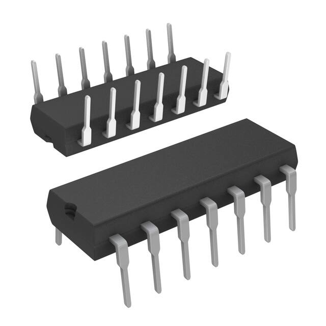
D, J, N, OR W PACKAGE
(TOP VIEW)
IN −
IN +
OFFSET 1N2
VCC −
OFFSET 2N2
IN +
IN −
description
OFFSET 1N2
NC
VCC −
NC
OFFSET 2N2
3
12
4
11
5
10
6
9
7
8
OFFSET 1N1
1 VCC +†
OUT
NC
OUT
2 VCC +†
OFFSET 2N1
4
3 2 1 20 19
18
5
17
6
16
7
15
8
14
9 10 11 12 13
OUT
NC
NC
NC
OUT
IN +
IN −
NC
OFFSET 2N1
2 V CC +†
The uA747C is characterized for operation from
0°C to 70°C; the uA747M is characterized for
operation over the full military temperature range
of −55°C to 125°C.
symbol (each amplifier)
IN −
13
IN +
IN −
NC
OFFSET 1N1
1 V CC +†
The high common-mode input voltage range and
the absence of latch-up make this amplifier ideal
for voltage-follower applications. The device is
short-circuit protected and the internal frequency
compensation ensures stability without external
components. A low-value potentiometer may be
connected between the offset null inputs to null out
the offset voltage as shown in Figure 2.
IN+
14
2
uA747m . . . FK PACKAGE
(TOP VIEW)
The uA747 is a dual general-purpose operational
amplifier featuring offset-voltage null capability.
Each half is electrically similar to uA741.
ÏÏÏ
ÏÏÏ
ÏÏÏ
ÏÏÏ
1
NC − No internal connection
+
† The two positive supply terminals (1 VCC + and 2 VCC +) are
connected together internally.
OUT
−
OFFSET N1
OFFSET N2
AVAILABLE OPTIONS
PACKAGE
TA
0°C
to
70°C
−55°C
to
125°C
VIO Max
AT 25°C
14-PIN
20-PIN
SMALL OUTLINE
(D)
CERAMIC DIP
(J)
PLASTIC DIP
(N)
FLAT PACK
(W)
CHIP CARRIER
(FK)
6 mV
uA747CD
—
uA747CN
—
—
5 mV
—
uA747MJ
—
uA747MW
uA747MFK
The D package is available taped and reeled. Add the suffix R to the device type, (i.e., uA747CDR).
Copyright 1990, Texas Instruments Incorporated
���
����� ��� ����������� �! "���#�� �! �� $�%&�"����� '��#(
���'�"�! "������ �� !$#"���"�����! $#� �)# �#��! �� �#*�! ��!����#��!
!���'��' +������,( ���'�"���� $��"#!!��- '�#! ��� �#"#!!���&, ��"&�'#
�#!���- �� �&& $����#�#�!(
•
POST OFFICE BOX 655303 DALLAS, TEXAS 75265
POST OFFICE BOX 1443 HOUSTON, TEXAS 77001
•
1
���������������
����
�
�����
����
���
����������������
��
�
SLOS009A − D971, FEBRUARY 1971 − REVISED OCTOBER 1990
schematic (each amplifier)
VCC +
IN −
OUT
IN +
OFFSET N2
OFFSET N1
VCC −
absolute maximum ratings over operating free-air temperature range (unless otherwise noted)
uA747M
UNIT
Supply voltage, VCC + (see Note 1)
uA747C
18
22
V
Supply voltage, VCC − (see Note 1)
−18
−22
V
Differential input voltage (see Note 2)
± 30
± 30
V
Input voltage any input (see Notes 1 and 3)
± 15
± 15
V
Voltage between any offset null terminal (N1/N2) and VCC −
± 0.5
± 0.5
V
unlimited
unlimited
Duration of output short circuit (see Note 4)
Continuous total dissipation
See Dissipation Rating Table
Operating free-air temperature range
Storage temperature range
0 to 70
−55 to 125
°C
−65 to 150
−65 to 150
°C
Case temperature for 60 seconds
FK package
260
°C
Lead temperature 1,6 mm (1/16 inch) from case for 60 seconds
J or W package
300
°C
Lead temperature 1,6 mm (1/16 inch) from case for 10 seconds
D or N package
NOTES: 1.
2.
3.
4.
°C
260
All voltage values, unless otherwise noted, are with respect to the midpoint between VCC + and VCC −.
Differential voltages are at the noninverting input terminal with respect to the inverting input terminal.
The magnitude of the input voltage must never exceed the magnitude of the supply voltage or 15 V, whichever is less.
The output may be shorted to ground or either power supply. For the uA747M only, the unlimited duration of the short circuit applies
at (or below) 125°C case temperature or 75°C free-air temperature.
DISSIPATION RATING TABLE
2
PACKAGE
TA ≤ 25°C
POWER RATING
DERATING
FACTOR
D
800 mW
7.6 mW/°C
DERATE
ABOVE TA
45°C
TA = 70°C
POWER RATING
TA = 125°C
POWER RATING
608 mW
—
FK
800 mW
11.0 mW/°C
77°C
800 mW
275 mW
275 mW
J
800 mW
11.0 mW/°C
77°C
800 mW
N
800 mW
9.2 mW/°C
63°C
736 mW
—
W
800 mW
8.0 mW/°C
50°C
640 mW
200 mW
•
POST OFFICE BOX 655303 DALLAS, TEXAS 75265
POST OFFICE BOX 1443 HOUSTON, TEXAS 77001
•
���������������
����
�
�����
����
���
����������������
��
�
SLOS009A − D971, FEBRUARY 1971 − REVISED OCTOBER 1990
electrical characteristics at specified free-air temperature, VCC ± = ±15 V
PARAMETER
VIO
Input offset voltage
∆VIO(adj)
Offset voltage
adjust range
IIO
Input offset current
IIB
Input bias current
VICR
VO(PP)
AVD
TA‡
TEST CONDITIONS†
uA747C
MIN
MAX
1
6
25°C
VO = 0
Full range
25°C
±15
25°C
20
25°C
80
25°C
±12
±12
RL= 10 kΩ
25°C
24
Maximum peak-to-peak
RL ≥ 10 kΩ
Full range
24
output voltage swing
RL= 2 kΩ
25°C
20
RL ≥ 2 kΩ
Full range
20
Large-signal differential
RL ≥ 2 kΩ,
25°C
25
voltage amplification
VO = ± 10 V
Full range
15
25°C
0.3
ri
Input resistance
ro
Output resistance
Ci
Input capacitance
CMRR
Common-mode
rejection ratio
VIC = VICR
25°C
70
Full range
70
kSVS
Supply-voltage
sensitivity
(∆VIO / ∆VCC)
VCC = ± 9 V to ± 15 V
25 C
25°C
Full range
IOS
Short-circuit
output current
ICC
Supply current
(each amplifier)
No load
1
5
6
±15
200
20
80
PD
Power dissipation
(each amplifier)
No load,
200
500
1500
±12
±13
24
20
nA
nA
28
24
26
mV
V
±12
28
UNIT
mV
500
500
±13
V
26
20
200
50
200
V/mV
25
2
0.3*
2
MΩ
25°C
75
75
Ω
25°C
1.4
1.4
pF
90
70
90
dB
70
30
150
30
150
150
150
25°C
± 25
± 40
± 25
± 40
25°C
1.7
2.8
1.7
2.8
Full range
VO = 0
MAX
800
Full range
See Note 5
TYP
300
Full range
input voltage range
MIN
7.5
Full range
Common-mode
uA747M
TYP
25°C
3.3
50
Full range
3.3
85
50
100
85
100
µV/V
mA
mA
mW
Vo1/Vo2
Channel separation
25°C
120
120
0
dB
† All characteristics are measured under open-loop conditions with zero common-mode input voltage unless otherwise specified.
‡ Full range for uA747C is 0°C to 70°C and for uA747M is − 55°C to 125°C.
*On products compliant to MIL-STD-883, Class B, this parameter is not production tested.
NOTE 5: This typical value applies only at frequencies above a few hundred hertz because of the effects of drift and thermal feedback.
operating characteristics, VCC ± = ± 15 V, TA = 25°C
PARAMETER
tr
SR
Rise time
TEST CONDITIONS
MIN
TYP
0.3
Overshoot factor
VI = 20 mV, RL = 2 kΩ, CL = 100 pF, See Figure 1
5%
Slew rate at unity gain
VI = 10 mV, RL = 2 kΩ, CL = 100 pF, See Figure 1
0.5
•
POST OFFICE BOX 655303 DALLAS, TEXAS 75265
POST OFFICE BOX 1443 HOUSTON, TEXAS 77001
•
MAX
UNIT
µs
V/µs
3
���������������
����
�
�����
����
���
����������������
��
�
SLOS009A − D971, FEBRUARY 1971 − REVISED OCTOBER 1990
PARAMETER MEASUREMENT INFORMATION
VI
Ï
−
+
Input
0V
INPUT VOLTAGE
WAVEFORM
RL = 2 kΩ
CL = 100 pF
TEST CIRCUIT
Figure 1. Rise Time, Overshoot, and Slew Rate
APPLICATION INFORMATION
IN −
−
IN +
+
OUT
OFFSET N2
OFFSET N1
10 kΩ
To VCC −
Figure 2. Input Offset Voltage Null Circuit
4
•
POST OFFICE BOX 655303 DALLAS, TEXAS 75265
POST OFFICE BOX 1443 HOUSTON, TEXAS 77001
•
OUT
���������������
����
�
�����
����
���
����������������
��
�
SLOS009A − D971, FEBRUARY 1971 − REVISED OCTOBER 1990
TYPICAL CHARACTERISTICS†
INPUT OFFSET CURRENT
vs
FREE-AIR TEMPERATURE
100
VCC ± = ± 15 V
IIIO
IO − Input Offset Current − nA
90
80
70
60
uA747C
50
40
30
20
10
0
−60 −40 −20 0
20 40 60 80 100 120 140
TA − Free-Air Temperature − C
Figure 3
INPUT BIAS CURRENT
vs
FREE-AIR TEMPERATURE
400
VCC ± = ± 15 V
IIB
I IB− Input Bias Current − nA
350
300
250
uA747C
200
150
100
50
0
−60 −40 −20 0
20 40 60 80 100 120 140
TA − Free-Air Temperature − C
Figure 4
† Data at high and low temperatures are applicable only within the rated operating free-air temperature range of the particular devices.
•
POST OFFICE BOX 655303 DALLAS, TEXAS 75265
POST OFFICE BOX 1443 HOUSTON, TEXAS 77001
•
5
���������������
����
�
�����
����
���
����������������
��
�
SLOS009A − D971, FEBRUARY 1971 − REVISED OCTOBER 1990
TYPICAL CHARACTERISTICS
MAXIMUM PEAK-TO-PEAK
OUTPUT VOLTAGE
vs
LOAD RESISTANCE
MAXIMUM PEAK-TO-PEAK
OUTPUT VOLTAGE
vs
FREQUENCY
VCC − Maximum Peak-to-Peak Output Voltage − V
VO(PP)
VCC
VCC − Maximum Peak-to-Peak Output Voltage − V
28
VCC ± = ± 15 V
TA = 25°C
26
24
22
20
18
16
14
ÁÁ
ÁÁ
ÁÁ
10
0.2
0.4
0.7 1
2
4
RL − Load Resistance − kΩ
7
VCC ± = ± 15 V
RL = 10 kΩ
TA = 25°C
36
32
28
24
20
16
12
ÁÁ
ÁÁ
ÁÁ
12
8
0.1
ÁÁÁÁÁ
ÁÁÁÁÁ
ÁÁÁÁÁ
40
10
8
4
0
100
1k
Figure 5
OPEN-LOOP LARGE-SIGNAL
DIFFERENTIAL
VOLTAGE AMPLIFICATION
vs
FREQUENCY
107
RL = 2 kΩ
TA = 25°C
AAVD
VD − Differential Voltage Amplification
A
AVD
VD − Differential Voltage Amplification V/mV
400
200
100
40
20
VCC ± = ± 15 V
RL = 2 kΩ
106
TA = 25°C
105
10 4
103
102
ÁÁ
ÁÁ
ÁÁ
101
1
10 −1
10
0
2
4
6
8
10 12 14 16
|VCC ±| − Supply Voltage − V
18
20
1
10
Figure 7
6
1M
Figure 6
OPEN-LOOP LARGE-SIGNAL
DIFFERENTIAL
VOLTAGE AMPLIFICATION
vs
SUPPLY VOLTAGE
ÁÁ
ÁÁ
10 k
100 k
f − Frequency − Hz
100
1 k 10 k 100 k 1 M
f − Frequency − Hz
Figure 8
•
POST OFFICE BOX 655303 DALLAS, TEXAS 75265
POST OFFICE BOX 1443 HOUSTON, TEXAS 77001
•
10 M 100 M
���������������
����
�
�����
����
���
����������������
��
�
SLOS009A − D971, FEBRUARY 1971 − REVISED OCTOBER 1990
TYPICAL CHARACTERISTICS
COMMON-MODE REJECTION RATIO
vs
FREQUENCY
OUTPUT VOLTAGE
vs
ELAPSED TIME
28
VCC ± = ± 15 V
RS = 50 Ω
TA = 25°C
90
24
VO
VO − Output Voltage − mV
80
70
60
50
ÁÁ
ÁÁ
40
30
20
20
90%
16
12
VCC ± = ± 15 V
RL = 2 kΩ
CL = 100 pF
TA = 25°C
8
4
10%
ÎÎ
0
10
0
1
10
100
1 k 10 k 100 k 1 M
f − Frequency − Hz
−4
10 M 100 M
ÎÎÎÎÎ
tr
0
0.5
Figure 9
1
1.5
t − Time − µs
2
2.5
Figure 10
VOLTAGE-FOLLOWER
LARGE-SIGNAL PULSE RESPONSE
8
VCC ± = ± 15 V
RL = 2 kΩ
CL = 100 pF
TA = 25°C
6
Input and Output Voltages − V
CMRR − Common-Mode Rejection Ratio − dB
100
4
Output
2
0
Input
−2
−4
−6
−8
0
10
20
30 40 50
t − Time − µs
60
70
80
90
Figure 11
•
POST OFFICE BOX 655303 DALLAS, TEXAS 75265
POST OFFICE BOX 1443 HOUSTON, TEXAS 77001
•
7
�PACKAGE OPTION ADDENDUM
www.ti.com
14-Aug-2021
PACKAGING INFORMATION
Orderable Device
Status
(1)
Package Type Package Pins Package
Drawing
Qty
Eco Plan
(2)
Lead finish/
Ball material
MSL Peak Temp
Op Temp (°C)
Device Marking
(3)
(4/5)
(6)
UA747CN
ACTIVE
PDIP
N
14
25
RoHS & Green
NIPDAU
N / A for Pkg Type
0 to 70
UA747CN
UA747CNE4
ACTIVE
PDIP
N
14
25
RoHS & Green
NIPDAU
N / A for Pkg Type
0 to 70
UA747CN
UA747CNE4
ACTIVE
PDIP
N
14
25
RoHS & Green
NIPDAU
N / A for Pkg Type
0 to 70
UA747CN
(1)
The marketing status values are defined as follows:
ACTIVE: Product device recommended for new designs.
LIFEBUY: TI has announced that the device will be discontinued, and a lifetime-buy period is in effect.
NRND: Not recommended for new designs. Device is in production to support existing customers, but TI does not recommend using this part in a new design.
PREVIEW: Device has been announced but is not in production. Samples may or may not be available.
OBSOLETE: TI has discontinued the production of the device.
(2)
RoHS: TI defines "RoHS" to mean semiconductor products that are compliant with the current EU RoHS requirements for all 10 RoHS substances, including the requirement that RoHS substance
do not exceed 0.1% by weight in homogeneous materials. Where designed to be soldered at high temperatures, "RoHS" products are suitable for use in specified lead-free processes. TI may
reference these types of products as "Pb-Free".
RoHS Exempt: TI defines "RoHS Exempt" to mean products that contain lead but are compliant with EU RoHS pursuant to a specific EU RoHS exemption.
Green: TI defines "Green" to mean the content of Chlorine (Cl) and Bromine (Br) based flame retardants meet JS709B low halogen requirements of


 工商网监
湘ICP备2023018690号
工商网监
湘ICP备2023018690号
