Product
Folder
Sample &
Buy
Support &
Community
Tools &
Software
Technical
Documents
uA7805, uA7808, uA7810
uA7812, uA7815, uA7824
SLVS056P – MAY 1976 – REVISED JANUARY 2015
µA78xx Fixed Positive Voltage Regulators
1 Features
3 Description
•
•
This series of fixed-voltage integrated-circuit voltage
regulators is designed for a wide range of
applications. These applications include on-card
regulation for elimination of noise and distribution
problems associated with single-point regulation.
Each of these regulators can deliver up to 1.5 A of
output current. The internal current-limiting and
thermal-shutdown features of these regulators
essentially make them immune to overload. In
addition to use as fixed-voltage regulators, these
devices can be used with external components to
obtain adjustable output voltages and currents, and
also can be used as the power-pass element in
precision regulators.
1
•
•
•
•
•
•
3-Terminal Regulators
Available in fixed 5-V/8-V/10-V/12-V/15-V/24-V
options
Output Current up to 1.5 A
Internal Thermal-Overload Protection
High Power-Dissipation Capability
Internal Short-Circuit Current Limiting
Output Transistor Safe-Area Compensation
Output Capacitor Not Needed for Stability
2 Applications
•
•
•
•
On-card Regulation
Portable Devices
Computing & Servers
Telecommunications
Device Information(1)
PART NUMBER
μA78xx
PACKAGE
BODY SIZE (NOM)
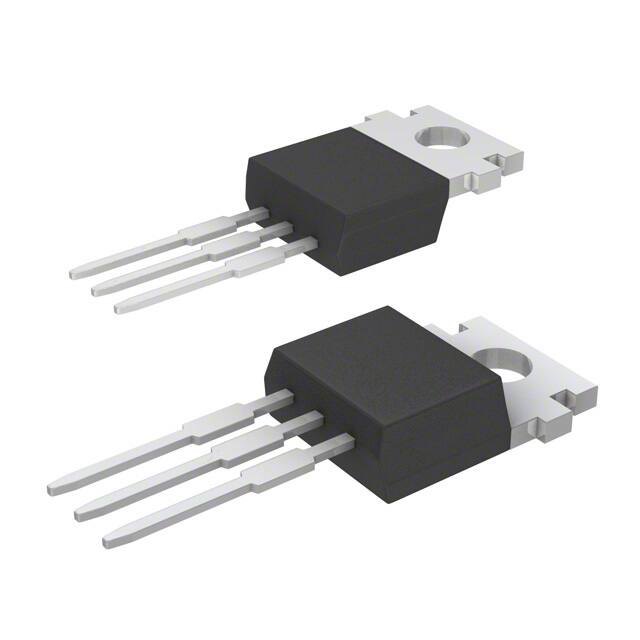
TO-220 (3)
10.16 mm x 8.82 mm
TO-220 (3)
10.16 mm x 8.82 mm
TO-263 (3)
10.06 mm x 9.02 mm
(1) For all available packages, see the orderable addendum at
the end of the data sheet.
4 Simplified Schematic
+V
0.33 µF
µA78xx
+VO
0.1 µF
1
An IMPORTANT NOTICE at the end of this data sheet addresses availability, warranty, changes, use in safety-critical applications,
intellectual property matters and other important disclaimers. PRODUCTION DATA.
�uA7805, uA7808, uA7810
uA7812, uA7815, uA7824
SLVS056P – MAY 1976 – REVISED JANUARY 2015
www.ti.com
Table of Contents
1
2
3
4
5
6
7
Features ..................................................................
Applications ...........................................................
Description .............................................................
Simplified Schematic.............................................
Revision History.....................................................
Pin Configuration and Functions .........................
Specifications.........................................................
7.1
7.2
7.3
7.4
7.5
7.6
7.7
7.8
7.9
7.10
7.11
1
1
1
1
2
3
4
Absolute Maximum Ratings ...................................... 4
ESD Ratings ............................................................ 4
Recommended Operating Conditions....................... 4
Thermal Information .................................................. 4
Electrical Characteristics — uA7805......................... 5
Electrical Characteristics — uA7808......................... 6
Electrical Characteristics — uA7810......................... 7
Electrical Characteristics — uA7812 ........................ 8
Electrical Characteristics — uA7815......................... 9
Electrical Characteristics — uA7824..................... 10
Typical Characteristics .......................................... 10
8
Detailed Description ............................................ 11
8.1
8.2
8.3
8.4
9
Overview .................................................................
Functional Schematic..............................................
Feature Description.................................................
Device Functional Modes........................................
11
11
11
11
Application and Implementation ........................ 12
9.1 Application Information............................................ 12
9.2 Typical Application ................................................. 12
10 Power Supply Recommendations ..................... 14
11 Layout................................................................... 15
11.1 Layout Guidelines ................................................. 15
11.2 Layout Example .................................................... 15
12 Device and Documentation Support ................. 15
12.1
12.2
12.3
12.4
Related Links ........................................................
Trademarks ...........................................................
Electrostatic Discharge Caution ............................
Glossary ................................................................
15
15
15
15
13 Mechanical, Packaging, and Orderable
Information ........................................................... 15
5 Revision History
Changes from Revision O (August 2012) to Revision P
Page
•
Added Applications, Device Information table, Pin Functions table, ESD Ratings table, Thermal Information table,
Typical Characteristics, Feature Description section, Device Functional Modes, Application and Implementation
section, Power Supply Recommendations section, Layout section, Device and Documentation Support section, and
Mechanical, Packaging, and Orderable Information section. ................................................................................................. 1
•
Deleted Ordering Information table. ....................................................................................................................................... 1
2
Submit Documentation Feedback
Copyright © 1976–2015, Texas Instruments Incorporated
Product Folder Links: uA7805 uA7808 uA7810 uA7812 uA7815 uA7824
�uA7805, uA7808, uA7810
uA7812, uA7815, uA7824
www.ti.com
SLVS056P – MAY 1976 – REVISED JANUARY 2015
6 Pin Configuration and Functions
E
ET
L
SO
OB
KCS OR KCT (TO-220) PACKAGE
(TOP VIEW)
OUTPUT
COMMON
INPUT
COMMON
COMMON
KC (TO-220) PACKAGE
(TOP VIEW)
TM
OB
E
ET
L
SO
KTT (TO-263) PACKAGE
(TOP VIEW)
COMMON
COMMON
KTE (PowerFLEX ) PACKAGE
(TOP VIEW)
OUTPUT
COMMON
INPUT
OUTPUT
COMMON
INPUT
OUTPUT
COMMON
INPUT
Pin Functions
PIN
NAME
NO.
TYPE
DESCRIPTION
COMMON
2
—
INPUT
1
I
Ground
Supply Input
OUTPUT
3
O
Voltage Output
Copyright © 1976–2015, Texas Instruments Incorporated
Submit Documentation Feedback
Product Folder Links: uA7805 uA7808 uA7810 uA7812 uA7815 uA7824
3
�uA7805, uA7808, uA7810
uA7812, uA7815, uA7824
SLVS056P – MAY 1976 – REVISED JANUARY 2015
www.ti.com
7 Specifications
7.1 Absolute Maximum Ratings
over virtual junction temperature range (unless otherwise noted)
MIN
Vl
Input voltage
TJ
Operating virtual junction temperature
Lead temperature
Tstg
MAX
μA7824C
40
All others
35
1,6 mm (1/16 in) from case for 10 s
Storage temperature range
–65
UNIT
V
150
°C
260
°C
150
°C
7.2 ESD Ratings
VALUE
V(ESD)
(1)
(2)
Electrostatic discharge
Human body model (HBM), per ANSI/ESDA/JEDEC JS-001, all pins (1)
3000
Charged device model (CDM), per JEDEC specification JESD22-C101,
all pins (2)
2000
UNIT
V
JEDEC document JEP155 states that 500-V HBM allows safe manufacturing with a standard ESD control process.
JEDEC document JEP157 states that 250-V CDM allows safe manufacturing with a standard ESD control process.
7.3 Recommended Operating Conditions
Vl
Input voltage
IO
Output current
TJ
Operating virtual junction temperature
MIN
MAX
μA7805
7
25
μA7808
10.5
25
μA7810
12.5
28
μA7812
14.5
30
μA7815
17.5
30
μA7824
27
UNIT
V
38
0
1.5
A
125
°C
7.4 Thermal Information
μA78XX
THERMAL METRIC (1)
RθJA
Junction-to-ambient thermal resistance
RθJC(top)
Junction-to-case (top) thermal resistance
RθJP(top)
Junction-to-exposed-pad thermal resistance
(1)
4
KTE
KCS, KCT,
KC
KTT
3 PINS
3 PINS
3 PINS
23
19
25.3
3
17
18
2.7
3
1.94
UNIT
°C/W
For more information about traditional and new thermal metrics, see the IC Package Thermal Metrics application report (SPRA953).
Submit Documentation Feedback
Copyright © 1976–2015, Texas Instruments Incorporated
Product Folder Links: uA7805 uA7808 uA7810 uA7812 uA7815 uA7824
�uA7805, uA7808, uA7810
uA7812, uA7815, uA7824
www.ti.com
SLVS056P – MAY 1976 – REVISED JANUARY 2015
7.5 Electrical Characteristics — uA7805
at specified virtual junction temperature, VI = 10 V, IO = 500 mA (unless otherwise noted)
PARAMETER
TEST CONDITIONS
IO = 5 mA to 1 A, VI = 7 V to 20 V,
PD ≤ 15 W
Output voltage
VI = 7 V to 25 V
Input voltage regulation
VI = 8 V to 12 V
VI = 8 V to 12 V, f = 120 Hz
Ripple rejection (2)
VI = 8 V to 12 V, f = 120 Hz (KCT)
IO = 5 mA to 1.5 A
Output voltage regulation
IO = 250 mA to 750 mA
TJ
μA7805C
(1)
MIN
TYP
25°C
4.8
5
0°C to 125°C
4.75
25°C
0°C to 125°C
62
UNIT
MAX
5.2
V
5.25
3
100
1
50
mV
78
dB
68
25°C
15
100
5
50
mV
Output resistance
f = 1 kHz
0°C to 125°C
0.017
Ω
Temperature coefficient of output voltage
IO = 5 mA
0°C to 125°C
–1.1
mV/°C
Output noise voltage
f = 10 Hz to 100 kHz
25°C
40
Dropout voltage
IO = 1 A
25°C
2
25°C
4.2
Bias current
Bias current change
VI = 7 V to 25 V
IO = 5 mA to 1 A
μV
V
8
1.3
0°C to 125°C
0.5
mA
mA
Short-circuit output current
25°C
750
mA
Peak output current
25°C
2.2
A
(1)
(2)
Pulse-testing techniques maintain the junction temperature as close to the ambient temperature as possible. Thermal effects must be
taken into account separately. All characteristics are measured with a 0.33-μF capacitor across the input and a 0.1-μF capacitor across
the output.
This parameter is validated by design and verified during product characterization. It is not tested in production.
Copyright © 1976–2015, Texas Instruments Incorporated
Submit Documentation Feedback
Product Folder Links: uA7805 uA7808 uA7810 uA7812 uA7815 uA7824
5
�uA7805, uA7808, uA7810
uA7812, uA7815, uA7824
SLVS056P – MAY 1976 – REVISED JANUARY 2015
www.ti.com
7.6 Electrical Characteristics — uA7808
at specified virtual junction temperature, VI = 14 V, IO = 500 mA (unless otherwise noted)
PARAMETER
TEST CONDITIONS
TJ
25°C
IO = 5 mA to 1 A, VI = 10.5 V to 23 V,
PD ≤ 15 W
0°C to 125°C
Output voltage
VI = 10.5 V to 25 V
Input voltage regulation
VI = 11 V to 17 V
VI = 11.5 V to 21.5 V, f = 120 Hz
(KCT)
IO = 5 mA to 1.5 A
Output voltage regulation
IO = 250 mA to 750 mA
MIN
TYP
MAX
7.7
8
8.3
7.6
25°C
VI = 11.5 V to 21.5 V, f = 120 Hz
Ripple rejection (2)
μA7808C
(1)
55
0°C to 125°C
25°C
8.4
6
160
2
80
UNIT
V
mV
72
dB
62
12
160
4
80
mV
Output resistance
f = 1 kHz
0°C to 125°C
0.016
Ω
Temperature coefficient of output voltage
IO = 5 mA
0°C to 125°C
–0.8
mV/°C
Output noise voltage
f = 10 Hz to 100 kHz
25°C
52
μV
Dropout voltage
IO = 1 A
25°C
2
V
25°C
4.3
Bias current
VI = 10.5 V to 25 V
Bias current change
IO = 5 mA to 1 A
8
1
0°C to 125°C
0.5
mA
mA
Short-circuit output current
25°C
450
mA
Peak output current
25°C
2.2
A
(1)
(2)
6
Pulse-testing techniques maintain the junction temperature as close to the ambient temperature as possible. Thermal effects must be
taken into account separately. All characteristics are measured with a 0.33-μF capacitor across the input and a 0.1-μF capacitor across
the output.
This parameter is validated by design and verified during product characterization. It is not tested in production.
Submit Documentation Feedback
Copyright © 1976–2015, Texas Instruments Incorporated
Product Folder Links: uA7805 uA7808 uA7810 uA7812 uA7815 uA7824
�uA7805, uA7808, uA7810
uA7812, uA7815, uA7824
www.ti.com
SLVS056P – MAY 1976 – REVISED JANUARY 2015
7.7 Electrical Characteristics — uA7810
at specified virtual junction temperature, VI = 17 V, IO = 500 mA (unless otherwise noted)
PARAMETER
TEST CONDITIONS
TJ
25°C
IO = 5 mA to 1 A, VI = 12.5 V to 25 V,
PD ≤ 15 W
0°C to 125°C
Output voltage
VI = 12.5 V to 28 V
Input voltage regulation
VI = 14 V to 20 V
Ripple rejection (2)
VI = 13 V to 23 V, f = 120 Hz
IO = 5 mA to 1.5 A
Output voltage regulation
IO = 250 mA to 750 mA
μA7810C
(1)
MIN
TYP
MAX
9.6
10
10.4
9.5
25°C
0°C to 125°C
55
25°C
UNIT
V
10.5
7
200
2
100
mV
71
dB
12
200
4
100
mV
Ω
Output resistance
f = 1 kHz
0°C to 125°C
0.018
Temperature coefficient of output voltage
IO = 5 mA
0°C to 125°C
–1
mV/°C
Output noise voltage
f = 10 Hz to 100 kHz
25°C
70
μV
Dropout voltage
IO = 1 A
25°C
2
25°C
4.3
Bias current
Bias current change
VI = 12.5 V to 28 V
IO = 5 mA to 1 A
V
8
1
0°C to 125°C
0.5
mA
mA
Short-circuit output current
25°C
400
mA
Peak output current
25°C
2.2
A
(1)
(2)
Pulse-testing techniques maintain the junction temperature as close to the ambient temperature as possible. Thermal effects must be
taken into account separately. All characteristics are measured with a 0.33-μF capacitor across the input and a 0.1-μF capacitor across
the output.
This parameter is validated by design and verified during product characterization. It is not tested in production.
Copyright © 1976–2015, Texas Instruments Incorporated
Submit Documentation Feedback
Product Folder Links: uA7805 uA7808 uA7810 uA7812 uA7815 uA7824
7
�uA7805, uA7808, uA7810
uA7812, uA7815, uA7824
SLVS056P – MAY 1976 – REVISED JANUARY 2015
www.ti.com
7.8 Electrical Characteristics — uA7812
at specified virtual junction temperature, VI = 19 V, IO = 500 mA (unless otherwise noted)
PARAMETER
TEST CONDITIONS
TJ
25°C
IO = 5 mA to 1 A, VI = 14.5 V to 27 V,
PD ≤ 15 W
0°C to 125°C
Output voltage
VI = 14.5 V to 30 V
Input voltage regulation
VI = 16 V to 22 V
VI = 15 V to 25 V, f = 120 Hz
Ripple rejection (2)
VI = 15 V to 25 V, f = 120 Hz (KCT)
IO = 5 mA to 1.5 A
Output voltage regulation
IO = 250 mA to 750 mA
μA7812C
(1)
MIN
TYP
MAX
11.5
12
12.5
11.4
25°C
0°C to 125°C
55
25°C
12.6
10
240
3
120
71
UNIT
V
mV
dB
61
12
240
4
120
mV
Ω
Output resistance
f = 1 kHz
0°C to 125°C
0.018
Temperature coefficient of output voltage
IO = 5 mA
0°C to 125°C
–1
mV/°C
Output noise voltage
f = 10 Hz to 100 kHz
25°C
75
μV
Dropout voltage
IO = 1 A
25°C
2
25°C
4.3
Bias current
VI = 14.5 V to 30 V
Bias current change
IO = 5 mA to 1 A
V
8
1
0°C to 125°C
0.5
mA
mA
Short-circuit output current
25°C
350
mA
Peak output current
25°C
2.2
A
(1)
(2)
8
Pulse-testing techniques maintain the junction temperature as close to the ambient temperature as possible. Thermal effects must be
taken into account separately. All characteristics are measured with a 0.33-μF capacitor across the input and a 0.1-μF capacitor across
the output.
This parameter is validated by design and verified during product characterization. It is not tested in production.
Submit Documentation Feedback
Copyright © 1976–2015, Texas Instruments Incorporated
Product Folder Links: uA7805 uA7808 uA7810 uA7812 uA7815 uA7824
�uA7805, uA7808, uA7810
uA7812, uA7815, uA7824
www.ti.com
SLVS056P – MAY 1976 – REVISED JANUARY 2015
7.9 Electrical Characteristics — uA7815
at specified virtual junction temperature, VI = 23 V, IO = 500 mA (unless otherwise noted)
PARAMETER
TEST CONDITIONS
IO = 5 mA to 1 A, VI = 17.5 V to 30 V,
PD ≤ 15 W
Output voltage
VI = 17.5 V to 30 V
Input voltage regulation
VI = 20 V to 26 V
TJ
μA7815C
(1)
MIN
TYP
25°C
14.4
15
0°C to 125°C
14.25
25°C
VI = 18.5 V to 28.5 V, f = 120 Hz
Ripple rejection (2)
VI = 18.5 V to 28.5 V, f = 120 Hz
(KCT)
IO = 5 mA to 1.5 A
Output voltage regulation
IO = 250 mA to 750 mA
54
0°C to 125°C
25°C
UNIT
MAX
15.6
V
15.75
11
300
3
150
mV
70
dB
60
12
300
4
150
mV
Ω
Output resistance
f = 1 kHz
0°C to 125°C
0.019
Temperature coefficient of output voltage
IO = 5 mA
0°C to 125°C
–1
mV/°C
Output noise voltage
f = 10 Hz to 100 kHz
25°C
90
μV
Dropout voltage
IO = 1 A
25°C
2
V
25°C
4.4
Bias current
Bias current change
VI = 17.5 V to 30 V
IO = 5 mA to 1 A
8
1
0°C to 125°C
0.5
mA
mA
Short-circuit output current
25°C
230
mA
Peak output current
25°C
2.1
A
(1)
(2)
Pulse-testing techniques maintain the junction temperature as close to the ambient temperature as possible. Thermal effects must be
taken into account separately. All characteristics are measured with a 0.33-μF capacitor across the input and a 0.1-μF capacitor across
the output.
This parameter is validated by design and verified during product characterization. It is not tested in production.
Copyright © 1976–2015, Texas Instruments Incorporated
Submit Documentation Feedback
Product Folder Links: uA7805 uA7808 uA7810 uA7812 uA7815 uA7824
9
�uA7805, uA7808, uA7810
uA7812, uA7815, uA7824
SLVS056P – MAY 1976 – REVISED JANUARY 2015
www.ti.com
7.10 Electrical Characteristics — uA7824
at specified virtual junction temperature, VI = 33 V, IO = 500 mA (unless otherwise noted)
PARAMETER
TEST CONDITIONS
IO = 5 mA to 1 A, VI = 27 V to 38 V,
PD ≤ 15 W
Output voltage
TJ
25°C
0°C to 125°C
VI = 27 V to 38 V
Input voltage regulation
VI = 28 V to 38 V, f = 120 Hz
0°C to 125°C
IO = 5 mA to 1.5 A
Output voltage regulation
MIN
TYP
23
24
22.8
25°C
VI = 30 V to 36 V
Ripple rejection (2)
μA7824C
(1)
50
25°C
IO = 250 mA to 750 mA
MAX
25
25.2
18
480
6
240
66
UNIT
V
mV
dB
12
480
4
240
mV
Output resistance
f = 1 kHz
0°C to 125°C
0.028
Ω
Temperature coefficient of output voltage
IO = 5 mA
0°C to 125°C
–1.5
mV/°C
Output noise voltage
f = 10 Hz to 100 kHz
25°C
170
μV
Dropout voltage
IO = 1 A
25°C
2
25°C
4.6
Bias current
VI = 27 V to 38 V
Bias current change
1
0°C to 125°C
IO = 5 mA to 1 A
V
8
0.5
mA
mA
Short-circuit output current
25°C
150
mA
Peak output current
25°C
2.1
A
(1)
(2)
Pulse-testing techniques maintain the junction temperature as close to the ambient temperature as possible. Thermal effects must be
taken into account separately. All characteristics are measured with a 0.33-μF capacitor across the input and a 0.1-μF capacitor across
the output.
This parameter is validated by design and verified during product characterization. It is not tested in production.
7.11 Typical Characteristics
4.5
Bias Current (mA)
4.0
3.5
3.0
IBIAS
2.5
0
5
10
VIN - VOUT (typ)
15
20
C001
Figure 1. µA7805 Bias Current vs Voltage Differential at 25°C
10
Submit Documentation Feedback
Copyright © 1976–2015, Texas Instruments Incorporated
Product Folder Links: uA7805 uA7808 uA7810 uA7812 uA7815 uA7824
�uA7805, uA7808, uA7810
uA7812, uA7815, uA7824
www.ti.com
SLVS056P – MAY 1976 – REVISED JANUARY 2015
8 Detailed Description
8.1 Overview
This series of fixed-voltage integrated-circuit voltage regulators is designed for a wide range of applications.
These applications include on-card regulation for elimination of noise and distribution problems associated with
single-point regulation. Each of these regulators can deliver up to 1.5 A of output current. The internal currentlimiting and thermal-shutdown features of these regulators essentially make them immune to overload. In
addition to use as fixed-voltage regulators, these devices can be used with external components to obtain
adjustable output voltages and currents, and also can be used as the power-pass element in precision
regulators.
8.2 Functional Schematic
INPUT
OUTPUT
COMMON
8.3 Feature Description
8.3.1 Thermal Overload
When the die temperature increases to unwanted levels, the device will reduce the output current to lower its
temperature. Under heavy loads, the device may alternate between on and off output states to regulate
temperature.
8.3.2 Short-Circuit Current Limiting
In the event of a short circuit, the device will limit its own current to safe levels by lowering the bias voltage of
internal pass transistors. If the device becomes overheated, the thermal overload protection will take over.
8.4 Device Functional Modes
8.4.1 Fixed-Output Mode
These devices are available in fixed-output voltages. See the orderable part list for the desired output.
Copyright © 1976–2015, Texas Instruments Incorporated
Submit Documentation Feedback
Product Folder Links: uA7805 uA7808 uA7810 uA7812 uA7815 uA7824
11
�uA7805, uA7808, uA7810
uA7812, uA7815, uA7824
SLVS056P – MAY 1976 – REVISED JANUARY 2015
www.ti.com
9 Application and Implementation
NOTE
Information in the following applications sections is not part of the TI component
specification, and TI does not warrant its accuracy or completeness. TI’s customers are
responsible for determining suitability of components for their purposes. Customers should
validate and test their design implementation to confirm system functionality.
9.1 Application Information
The following section shows application details of the µA78xx as a linear regulator.
9.2 Typical Application
+V
+VO
µA78xx
0.33 µF
0.1 µF
Figure 2. Fixed-Output Regulator
9.2.1 Design Requirements
• Input supply capacitor recommended for filtering noise on the input
• Output supply decoupling capacitor for stabilizing the output
9.2.2 Detailed Design Procedure
9.2.2.1 Operation With a Load Common to a Voltage of Opposite Polarity
In many cases, a regulator powers a load that is not connected to ground but, instead, is connected to a voltage
source of opposite polarity (e.g., operational amplifiers, level-shifting circuits, etc.). In these cases, a clamp diode
should be connected to the regulator output as shown in Figure 3. This protects the regulator from output polarity
reversals during startup and short-circuit operation.
+VI
+VO
µA78xx
1N4001
or
Equivalent
−VO
Figure 3. Output Polarity-Reversal-Protection Circuit
9.2.2.2 Reverse-Bias Protection
Occasionally, the input voltage to the regulator can collapse faster than the output voltage. This can occur, for
example, when the input supply is crowbarred during an output overvoltage condition. If the output voltage is
greater than approximately 7 V, the emitter-base junction of the series-pass element (internal or external) could
break down and be damaged. To prevent this, a diode shunt can be used as shown in Figure 4.
12
Submit Documentation Feedback
Copyright © 1976–2015, Texas Instruments Incorporated
Product Folder Links: uA7805 uA7808 uA7810 uA7812 uA7815 uA7824
�uA7805, uA7808, uA7810
uA7812, uA7815, uA7824
www.ti.com
SLVS056P – MAY 1976 – REVISED JANUARY 2015
Typical Application (continued)
VI
+VO
µA78xx
Figure 4. Reverse-Bias-Protection Circuit
9.2.3 Application Curves
2.40
Voltage Loss (V)
2.20
2.00
1.80
1.60
1.40
1.20
1.00
0.00
Voltage Loss
0.25
0.50
0.75
1.00
1.25
1.50
Output Current (A)
C001
Figure 5. µA7805 Voltage Loss vs Output Current at 25°C
9.2.4 General Configurations
IN
+
OUT
G
µ
VI
A78xx
IL
COM
−VO
−
Figure 6. Positive Regulator in Negative Configuration (VI Must Float)
Input
Output
µA78xx
IO
R1
0.1 µF
0.33 µF
R2
A:
The following formula is used when Vxx is the nominal output voltage (output to common) of the fixed regulators
æV
ö
VO = VXX + ç XX + IQ ÷ R2
è R1
ø
Figure 7. Adjustable-Output Regulator
Copyright © 1976–2015, Texas Instruments Incorporated
Submit Documentation Feedback
Product Folder Links: uA7805 uA7808 uA7810 uA7812 uA7815 uA7824
13
�uA7805, uA7808, uA7810
uA7812, uA7815, uA7824
SLVS056P – MAY 1976 – REVISED JANUARY 2015
www.ti.com
Typical Application (continued)
Input
µA78xx
R1
VO(Reg)
0.33 µF
Output
IO
IO = (VO/R1) + IO Bias Current
Figure 8. Current Regulator
1N4001
20-V Input
VO = 15 V
µA7815C
0.33 µF
1 µF
2 µF
−20-V Input
1N4001
0.1 µF
0.1 µF
1N4001
VO = −15 V
µA7915C
1N4001
Figure 9. Regulated Dual Supply
10 Power Supply Recommendations
See Recommended Operating Conditions for the recommended power supply voltages for each variation of the
μA78xx device. Different orderable part numbers will be able to tolerate different levels of voltage. It is also
recommended to have a decoupling capacitor on the output of the μA78xx device's power supply to limit noise
on the device input.
14
Submit Documentation Feedback
Copyright © 1976–2015, Texas Instruments Incorporated
Product Folder Links: uA7805 uA7808 uA7810 uA7812 uA7815 uA7824
�uA7805, uA7808, uA7810
uA7812, uA7815, uA7824
www.ti.com
SLVS056P – MAY 1976 – REVISED JANUARY 2015
11 Layout
11.1 Layout Guidelines
Keep trace widths large enough to eliminate problematic I×R voltage drops at the input and output terminals.
Input decoupling capacitors should be placed as close to the μA78XX as possible.
11.2 Layout Example
COMMON
OUTPUT
Ground
COMMON
INPUT
�����PF
����PF
Ground
Figure 10. Layout Diagram
12 Device and Documentation Support
12.1 Related Links
The table below lists quick access links. Categories include technical documents, support and community
resources, tools and software, and quick access to sample or buy.
Table 1. Related Links
PARTS
PRODUCT FOLDER
SAMPLE & BUY
TECHNICAL
DOCUMENTS
TOOLS &
SOFTWARE
SUPPORT &
COMMUNITY
μA7805
Click here
Click here
Click here
Click here
Click here
uA7808
Click here
Click here
Click here
Click here
Click here
uA7810
Click here
Click here
Click here
Click here
Click here
uA7812
Click here
Click here
Click here
Click here
Click here
uA7815
Click here
Click here
Click here
Click here
Click here
uA7924
Click here
Click here
Click here
Click here
Click here
12.2 Trademarks
12.3 Electrostatic Discharge Caution
These devices have limited built-in ESD protection. The leads should be shorted together or the device placed in conductive foam
during storage or handling to prevent electrostatic damage to the MOS gates.
12.4 Glossary
SLYZ022 — TI Glossary.
This glossary lists and explains terms, acronyms, and definitions.
13 Mechanical, Packaging, and Orderable Information
The following pages include mechanical, packaging, and orderable information. This information is the most
current data available for the designated devices. This data is subject to change without notice and revision of
this document. For browser-based versions of this data sheet, refer to the left-hand navigation.
Copyright © 1976–2015, Texas Instruments Incorporated
Submit Documentation Feedback
Product Folder Links: uA7805 uA7808 uA7810 uA7812 uA7815 uA7824
15
�PACKAGE OPTION ADDENDUM
www.ti.com
10-Dec-2022
PACKAGING INFORMATION
Orderable Device
Status
(1)
Package Type Package Pins Package
Drawing
Qty
Eco Plan
(2)
Lead finish/
Ball material
MSL Peak Temp
Op Temp (°C)
Device Marking
(3)
Samples
(4/5)
(6)
UA7805CKCS
ACTIVE
TO-220
KCS
3
50
RoHS & Green
SN
N / A for Pkg Type
0 to 125
UA7805C
Samples
UA7805CKCSE3
ACTIVE
TO-220
KCS
3
50
RoHS & Green
SN
N / A for Pkg Type
0 to 125
UA7805C
Samples
UA7805CKCT
LIFEBUY
TO-220
KCT
3
50
RoHS &
Non-Green
SN
N / A for Pkg Type
0 to 125
UA7805C
UA7805CKTTR
ACTIVE
DDPAK/
TO-263
KTT
3
500
RoHS & Green
SN
Level-3-245C-168 HR
0 to 125
UA7805C
Samples
UA7805CKTTRG3
ACTIVE
DDPAK/
TO-263
KTT
3
500
RoHS & Green
SN
Level-3-245C-168 HR
0 to 125
UA7805C
Samples
UA7808CKCS
LIFEBUY
TO-220
KCS
3
50
RoHS & Green
SN
N / A for Pkg Type
0 to 125
UA7808C
UA7808CKCSE3
LIFEBUY
TO-220
KCS
3
50
RoHS & Green
SN
N / A for Pkg Type
0 to 125
UA7808C
UA7808CKCT
ACTIVE
TO-220
KCT
3
50
RoHS &
Non-Green
SN
N / A for Pkg Type
0 to 125
UA7808C
Samples
UA7808CKTTR
ACTIVE
DDPAK/
TO-263
KTT
3
500
RoHS & Green
SN
Level-3-245C-168 HR
0 to 125
UA7808C
Samples
UA7810CKCS
ACTIVE
TO-220
KCS
3
50
RoHS & Green
SN
N / A for Pkg Type
0 to 125
UA7810C
Samples
UA7810CKCSE3
ACTIVE
TO-220
KCS
3
50
RoHS & Green
SN
N / A for Pkg Type
0 to 125
UA7810C
Samples
UA7810CKTTR
ACTIVE
DDPAK/
TO-263
KTT
3
500
RoHS & Green
SN
Level-3-245C-168 HR
0 to 125
UA7810C
Samples
UA7810CKTTRG3
ACTIVE
DDPAK/
TO-263
KTT
3
500
RoHS & Green
SN
Level-3-245C-168 HR
0 to 125
UA7810C
Samples
UA7812CKCS
ACTIVE
TO-220
KCS
3
50
RoHS & Green
SN
N / A for Pkg Type
0 to 125
UA7812C
Samples
UA7812CKCSE3
ACTIVE
TO-220
KCS
3
50
RoHS & Green
SN
N / A for Pkg Type
0 to 125
UA7812C
Samples
UA7812CKCT
LIFEBUY
TO-220
KCT
3
50
RoHS &
Non-Green
SN
N / A for Pkg Type
0 to 125
UA7812C
UA7812CKTTR
ACTIVE
DDPAK/
TO-263
KTT
3
500
RoHS & Green
SN
Level-3-245C-168 HR
0 to 125
UA7812C
Samples
UA7812CKTTRG3
ACTIVE
DDPAK/
TO-263
KTT
3
500
RoHS & Green
SN
Level-3-245C-168 HR
0 to 125
UA7812C
Samples
Addendum-Page 1
�PACKAGE OPTION ADDENDUM
www.ti.com
Orderable Device
10-Dec-2022
Status
(1)
Package Type Package Pins Package
Drawing
Qty
Eco Plan
(2)
Lead finish/
Ball material
MSL Peak Temp
Op Temp (°C)
Device Marking
(3)
Samples
(4/5)
(6)
UA7815CKCS
ACTIVE
TO-220
KCS
3
50
RoHS & Green
SN
N / A for Pkg Type
0 to 125
UA7815C
Samples
UA7815CKCSE3
ACTIVE
TO-220
KCS
3
50
RoHS & Green
SN
N / A for Pkg Type
0 to 125
UA7815C
Samples
UA7815CKCT
LIFEBUY
TO-220
KCT
3
50
RoHS &
Non-Green
SN
N / A for Pkg Type
0 to 125
UA7815C
UA7815CKTTR
LIFEBUY
DDPAK/
TO-263
KTT
3
500
RoHS & Green
SN
Level-3-245C-168 HR
0 to 125
UA7815C
UA7824CKCS
LIFEBUY
TO-220
KCS
3
50
RoHS & Green
SN
N / A for Pkg Type
0 to 125
UA7824C
UA7824CKCSE3
LIFEBUY
TO-220
KCS
3
50
RoHS & Green
SN
N / A for Pkg Type
0 to 125
UA7824C
UA7824CKTTR
ACTIVE
DDPAK/
TO-263
KTT
3
500
RoHS & Green
SN
Level-3-245C-168 HR
0 to 125
UA7824C
(1)
The marketing status values are defined as follows:
ACTIVE: Product device recommended for new designs.
LIFEBUY: TI has announced that the device will be discontinued, and a lifetime-buy period is in effect.
NRND: Not recommended for new designs. Device is in production to support existing customers, but TI does not recommend using this part in a new design.
PREVIEW: Device has been announced but is not in production. Samples may or may not be available.
OBSOLETE: TI has discontinued the production of the device.
(2)
RoHS: TI defines "RoHS" to mean semiconductor products that are compliant with the current EU RoHS requirements for all 10 RoHS substances, including the requirement that RoHS substance
do not exceed 0.1% by weight in homogeneous materials. Where designed to be soldered at high temperatures, "RoHS" products are suitable for use in specified lead-free processes. TI may
reference these types of products as "Pb-Free".
RoHS Exempt: TI defines "RoHS Exempt" to mean products that contain lead but are compliant with EU RoHS pursuant to a specific EU RoHS exemption.
Green: TI defines "Green" to mean the content of Chlorine (Cl) and Bromine (Br) based flame retardants meet JS709B low halogen requirements of


 工商网监
湘ICP备2023018690号
工商网监
湘ICP备2023018690号
