µ������ ��� ��
����
��
������ ����������
SLVS060K − JUNE 1976 − REVISED APRIL 2005
D 3-Terminal Regulators
D Output Current Up To 500 mA
D No External Components
D High Power-Dissipation Capability
D Internal Short-Circuit Current Limiting
D Output Transistor Safe-Area Compensation
µA79M05, µA79M08 . . . KTP PACKAGE
(TOP VIEW)
INPUT
µA79M05 . . . KC (TO-220) PACKAGE
(TOP VIEW)
INPUT
OUTPUT
INPUT
COMMON
OUTPUT
INPUT
COMMON
INPUT
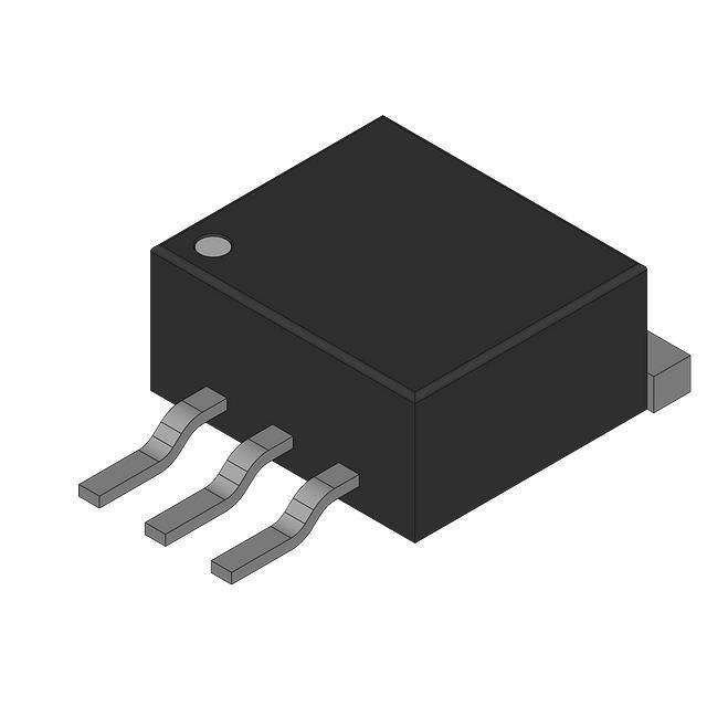
µA79M05 . . . KCS (TO-220) PACKAGE
(TOP VIEW)
OUTPUT
INPUT
COMMON
description/ordering information
This series of fixed-negative-voltage integrated-circuit voltage regulators is designed to complement the
µA78M00 series in a wide range of applications. These applications include on-card regulation for elimination
of noise and distribution problems associated with single-point regulation. Each of these regulators delivers up
to 500 mA of output current. The internal current-limiting and thermal-shutdown features of these regulators
essentially make them immune to overload. In addition to use as fixed-voltage regulators, these devices can
be used with external components to obtain adjustable output voltages and currents, and also as the
power-pass element in precision regulators.
ORDERING INFORMATION
TJ
0°C to 125°C
VO(NOM)
(V)
−5
ORDERABLE
PART NUMBER
PACKAGE†
PowerFLEX (KTP)
Reel of 3000
µA79M05CKTPR
TO-220 (KC)
Tube of 50
µA79M05CKC
TO-220, short shoulder (KCS)
Tube of 20
µA79M05CKCS
TOP-SIDE
MARKING
µA79M05C
µA79M05C
A79M05C
−8
PowerFLEX (KTP)
Reel of 3000
µA79M08CKTPR
µA79M08C
† Package drawings, standard packing quantities, thermal data, symbolization, and PCB design guidelines are available at
www.ti.com/sc/package.
Please be aware that an important notice concerning availability, standard warranty, and use in critical applications of
Texas Instruments semiconductor products and disclaimers thereto appears at the end of this data sheet.
PowerFLEX is a trademark of Texas Instruments.
Copyright 2005, Texas Instruments Incorporated
������� �
���� ����������� �� ����!�� �� �� "�#$������� %��!&
���%���� ������� �� �"!����������� "!� �'! �!��� �� �!(�� ������!���
����%��% )������*& ���%������ "���!����+ %�!� ��� �!�!�����$* ���$�%!
�!����+ �� �$$ "����!�!��&
POST OFFICE BOX 655303
• DALLAS, TEXAS 75265
1
�µ������ ��� ��
����
��
������ ����������
SLVS060K − JUNE 1976 − REVISED APRIL 2005
schematic
COMMON
4.5 kΩ
to 6.3 kΩ
1.7 kΩ
to 18 kΩ
OUTPUT
0.1 Ω
0.2 Ω
INPUT
Resistor values shown are nominal.
absolute maximum ratings over virtual junction temperature range (unless otherwise noted)†
Input voltage, VI . . . . . . . . . . . . . . . . . . . . . . . . . . . . . . . . . . . . . . . . . . . . . . . . . . . . . . . . . . . . . . . . . . . . . . . . . . . 35 V
Operating virtual junction temperature, TJ . . . . . . . . . . . . . . . . . . . . . . . . . . . . . . . . . . . . . . . . . . . . . . . . . . . 150°C
Lead temperature 1,6 mm (1/16 inch) from case for 10 seconds . . . . . . . . . . . . . . . . . . . . . . . . . . . . . . . 260°C
Storage temperature range, Tstg . . . . . . . . . . . . . . . . . . . . . . . . . . . . . . . . . . . . . . . . . . . . . . . . . . . . −65°C to 150°C
† Stresses beyond those listed under “absolute maximum ratings” may cause permanent damage to the device. These are stress ratings only, and
functional operation of the device at these or any other conditions beyond those indicated under “recommended operating conditions” is not
implied. Exposure to absolute-maximum-rated conditions for extended periods may affect device reliability.
package thermal data (see Note 1)
PowerFLEX (KTP)
High K, JESD 51-5
θJC
19°C/W
TO-220 (KC/KCS)
High K, JESD 51-5
17°C/W
PACKAGE
BOARD
θJA
28°C/W
19°C/W
θJP‡
1.4°C/W
3°C/W
NOTE 1: Maximum power dissipation is a function of TJ(max), θJA, and TA. The maximum allowable power dissipation at any allowable ambient
temperature is PD = (TJ(max) − TA)/θJA. Operating at the absolute maximum TJ of 150°C can affect reliability.
‡ For packages with exposed thermal pads, such as QFN, PowerPAD, or PowerFLEX, θJP is defined as the thermal resistance between the die
junction and the bottom of the exposed pad.
2
POST OFFICE BOX 655303
• DALLAS, TEXAS 75265
�µ������ ��� ��
����
��
������ ����������
SLVS060K − JUNE 1976 − REVISED APRIL 2005
recommended operating conditions
VI
Input voltage
IO
TJ
Output current
MIN
MAX
µA79M05C
−7
−25
µA79M08C
−10.5
−25
Operating virtual junction temperature
0
UNIT
V
500
mA
125
°C
electrical characteristics at specified virtual junction temperature, VI = −10 V, IO = 350 mA, TJ = 25°C
(unless otherwise noted)
µA79M05C
TEST CONDITIONS†
PARAMETER
Output voltage
VI = −7 V to −25 V,
Input voltage regulation
VI = −7 V to −25 V
VI = −8 V to −18 V
Ripple rejection
VI = −8 V to −18 V,
f = 120 Hz
Output voltage regulation
IO = 5 mA to 500 mA
IO = 5 mA to 350 mA
Temperature coefficient
of output voltage
IO = 5 mA,
Output noise voltage
f = 10 Hz to 100 kHz
IO = 5 mA to 350 mA
IO = 100 mA,
IO = 300 mA
TJ = 0°C to 125°C
TJ = 0°C to 125°C
MIN
TYP
MAX
−4.8
−5
−5.2
−4.75
−5.25
7
50
3
30
54
100
mV
−0.4
mV/°C
125
µV
1.1
Bias current
1
Bias current change
VI = −8 V to −18 V,
IO = 5 mA to 350 mA,
Short-circuit output current
VI = −30 V
mV
dB
60
50
Dropout voltage
V
50
75
TJ = 0°C to 125°C
UNIT
TJ = 0°C to 125°C
TJ = 0°C to 125°C
V
2
mA
0.4
0.4
140
mA
mA
Peak output current
0.65
A
† Pulse-testing techniques maintain TJ as close to TA as possible. Thermal effects must be taken into account separately. All characteristics are
measured with a 2-µF capacitor across the input and a 1-µF capacitor across the output.
POST OFFICE BOX 655303
• DALLAS, TEXAS 75265
3
�µ������ ��� ��
����
��
������ ����������
SLVS060K − JUNE 1976 − REVISED APRIL 2005
electrical characteristics at specified virtual junction temperature, VI = −19 V, IO = 350 mA, TJ = 25°C
(unless otherwise noted)
µA79M08C
TEST CONDITIONS†
PARAMETER
Output voltage
VI = −10.5 V to −25 V,
Input voltage regulation
VI = −10.5 V to −25 V
VI = −11 V to −21 V
Ripple rejection
VI = −11.5 V to −21.5 V,
f = 120 Hz
Output voltage regulation
IO = 5 mA to 500 mA
IO = 5 mA to 350 mA
Temperature coefficient
of output voltage
IO = 5 mA,
Output noise voltage
Dropout voltage
IO = 5 mA to 350 mA
IO = 100 mA,
IO = 300 mA
TJ = 0°C to 125°C
TJ = 0°C to 125°C
MIN
TYP
MAX
−7.7
−8
−8.3
−7.6
−8.4
8
80
4
50
V
mV
50
54
dB
59
90
160
mV
60
TJ = 0°C to 125°C
UNIT
−0.6
mV/°C
f = 10 Hz to 100 kHz
200
µV
IO = 5 mA
1.1
Bias current
1
Bias current change
VI = −10.5 V to −25 V,
IO = 5 mA to 350 mA,
Short-circuit output current
VI = −30 V
TJ = 0°C to 125°C
TJ = 0°C to 125°C
V
2
mA
0.4
0.4
140
mA
mA
Peak output current
0.65
A
† Pulse-testing techniques maintain TJ as close to TA as possible. Thermal effects must be taken into account separately. All characteristics are
measured with a 2-µF capacitor across the input and a 1-µF capacitor across the output.
4
POST OFFICE BOX 655303
• DALLAS, TEXAS 75265
�PACKAGE OPTION ADDENDUM
www.ti.com
21-May-2013
PACKAGING INFORMATION
Orderable Device
Status
(1)
Package Type Package Pins Package
Drawing
Qty
Eco Plan
Lead/Ball Finish
(2)
MSL Peak Temp
Op Temp (°C)
Device Marking
(3)
(4/5)
7704001HA
OBSOLETE
CFP
U
10
TBD
Call TI
Call TI
-55 to 125
UA79M05CKC
OBSOLETE
TO-220
KC
3
TBD
Call TI
Call TI
0 to 125
UA79M05C
UA79M05CKCE3
OBSOLETE
TO-220
KC
3
TBD
Call TI
Call TI
0 to 125
UA79M05C
UA79M05CKCS
ACTIVE
TO-220
KCS
3
50
Pb-Free
(RoHS)
CU SN
N / A for Pkg Type
0 to 125
UA79M05C
UA79M05CKCSE3
ACTIVE
TO-220
KCS
3
50
Pb-Free
(RoHS)
CU SN
N / A for Pkg Type
0 to 125
UA79M05C
UA79M05CKTPR
OBSOLETE
PFM
KTP
2
TBD
Call TI
Call TI
0 to 125
UA79M05C
UA79M05CKTPRG3
OBSOLETE
PFM
KTP
2
TBD
Call TI
Call TI
0 to 125
UA79M05C
UA79M05CKVURG3
ACTIVE
TO-252
KVU
3
Green (RoHS
& no Sb/Br)
CU SN
Level-3-260C-168 HR
0 to 125
79M05C
UA79M05MUB
OBSOLETE
CFP
U
10
TBD
Call TI
Call TI
-55 to 125
UA79M08CKC
OBSOLETE
TO-220
KC
3
TBD
Call TI
Call TI
0 to 125
UA79M08CKTPR
OBSOLETE
PFM
KTP
2
TBD
Call TI
Call TI
0 to 125
UA79M08C
UA79M08CKTPRG3
OBSOLETE
PFM
KTP
2
UA79M08CKVURG3
ACTIVE
TO-252
KVU
3
2500
2500
TBD
Call TI
Call TI
0 to 125
UA79M08C
Green (RoHS
& no Sb/Br)
CU SN
Level-3-260C-168 HR
0 to 125
79M08C
(1)
The marketing status values are defined as follows:
ACTIVE: Product device recommended for new designs.
LIFEBUY: TI has announced that the device will be discontinued, and a lifetime-buy period is in effect.
NRND: Not recommended for new designs. Device is in production to support existing customers, but TI does not recommend using this part in a new design.
PREVIEW: Device has been announced but is not in production. Samples may or may not be available.
OBSOLETE: TI has discontinued the production of the device.
(2)
Eco Plan - The planned eco-friendly classification: Pb-Free (RoHS), Pb-Free (RoHS Exempt), or Green (RoHS & no Sb/Br) - please check http://www.ti.com/productcontent for the latest availability
information and additional product content details.
TBD: The Pb-Free/Green conversion plan has not been defined.
Pb-Free (RoHS): TI's terms "Lead-Free" or "Pb-Free" mean semiconductor products that are compatible with the current RoHS requirements for all 6 substances, including the requirement that
lead not exceed 0.1% by weight in homogeneous materials. Where designed to be soldered at high temperatures, TI Pb-Free products are suitable for use in specified lead-free processes.
Pb-Free (RoHS Exempt): This component has a RoHS exemption for either 1) lead-based flip-chip solder bumps used between the die and package, or 2) lead-based die adhesive used between
the die and leadframe. The component is otherwise considered Pb-Free (RoHS compatible) as defined above.
Green (RoHS & no Sb/Br): TI defines "Green" to mean Pb-Free (RoHS compatible), and free of Bromine (Br) and Antimony (Sb) based flame retardants (Br or Sb do not exceed 0.1% by weight
in homogeneous material)
Addendum-Page 1
Samples
�PACKAGE OPTION ADDENDUM
www.ti.com
21-May-2013
(3)
MSL, Peak Temp. -- The Moisture Sensitivity Level rating according to the JEDEC industry standard classifications, and peak solder temperature.
(4)
There may be additional marking, which relates to the logo, the lot trace code information, or the environmental category on the device.
(5)
Multiple Device Markings will be inside parentheses. Only one Device Marking contained in parentheses and separated by a "~" will appear on a device. If a line is indented then it is a continuation
of the previous line and the two combined represent the entire Device Marking for that device.
Important Information and Disclaimer:The information provided on this page represents TI's knowledge and belief as of the date that it is provided. TI bases its knowledge and belief on information
provided by third parties, and makes no representation or warranty as to the accuracy of such information. Efforts are underway to better integrate information from third parties. TI has taken and
continues to take reasonable steps to provide representative and accurate information but may not have conducted destructive testing or chemical analysis on incoming materials and chemicals.
TI and TI suppliers consider certain information to be proprietary, and thus CAS numbers and other limited information may not be available for release.
In no event shall TI's liability arising out of such information exceed the total purchase price of the TI part(s) at issue in this document sold by TI to Customer on an annual basis.
Addendum-Page 2
�PACKAGE MATERIALS INFORMATION
www.ti.com
29-May-2013
TAPE AND REEL INFORMATION
*All dimensions are nominal
Device
Package Package Pins
Type Drawing
SPQ
Reel
Reel
A0
Diameter Width (mm)
(mm) W1 (mm)
B0
(mm)
K0
(mm)
P1
(mm)
W
Pin1
(mm) Quadrant
UA79M05CKVURG3
TO-252
KVU
3
2500
330.0
16.4
6.9
10.5
2.7
8.0
16.0
Q2
UA79M08CKVURG3
TO-252
KVU
3
2500
330.0
16.4
6.9
10.5
2.7
8.0
16.0
Q2
Pack Materials-Page 1
�PACKAGE MATERIALS INFORMATION
www.ti.com
29-May-2013
*All dimensions are nominal
Device
Package Type
Package Drawing
Pins
SPQ
Length (mm)
Width (mm)
Height (mm)
UA79M05CKVURG3
TO-252
KVU
3
2500
340.0
340.0
38.0
UA79M08CKVURG3
TO-252
KVU
3
2500
340.0
340.0
38.0
Pack Materials-Page 2
�PACKAGE OUTLINE
KCS0003B
TO-220 - 19.65 mm max height
SCALE 0.850
TO-220
4.7
4.4
10.36
9.96
1.32
1.22
2.9
2.6
6.5
6.1
8.55
8.15
(6.3)
( 3.84)
12.5
12.1
19.65 MAX
9.25
9.05
3X
3.9 MAX
13.12
12.70
3
1
3X
3X
0.47
0.34
0.90
0.77
2.79
2.59
2X 2.54
1.36
1.23
5.08
4222214/A 10/2015
NOTES:
1. All controlling linear dimensions are in inches. Dimensions in brackets are in millimeters. Any dimension in brackets or parenthesis are for
reference only. Dimensioning and tolerancing per ASME Y14.5M.
2. This drawing is subject to change without notice.
3. Reference JEDEC registration TO-220.
www.ti.com
�EXAMPLE BOARD LAYOUT
KCS0003B
TO-220 - 19.65 mm max height
TO-220
0.07 MAX
ALL AROUND
3X
2X (1.7)
METAL
(1.2)
2X SOLDER MASK
OPENING
(1.7)
R (0.05)
SOLDER MASK
OPENING
2
1
(2.54)
3
0.07 MAX
ALL AROUND
(5.08)
LAND PATTERN EXAMPLE
NON-SOLDER MASK DEFINED
SCALE:15X
4222214/A 10/2015
www.ti.com
���IMPORTANT NOTICE FOR TI DESIGN INFORMATION AND RESOURCES
Texas Instruments Incorporated (‘TI”) technical, application or other design advice, services or information, including, but not limited to,
reference designs and materials relating to evaluation modules, (collectively, “TI Resources”) are intended to assist designers who are
developing applications that incorporate TI products; by downloading, accessing or using any particular TI Resource in any way, you
(individually or, if you are acting on behalf of a company, your company) agree to use it solely for this purpose and subject to the terms of
this Notice.
TI’s provision of TI Resources does not expand or otherwise alter TI’s applicable published warranties or warranty disclaimers for TI
products, and no additional obligations or liabilities arise from TI providing such TI Resources. TI reserves the right to make corrections,
enhancements, improvements and other changes to its TI Resources.
You understand and agree that you remain responsible for using your independent analysis, evaluation and judgment in designing your
applications and that you have full and exclusive responsibility to assure the safety of your applications and compliance of your applications
(and of all TI products used in or for your applications) with all applicable regulations, laws and other applicable requirements. You
represent that, with respect to your applications, you have all the necessary expertise to create and implement safeguards that (1)
anticipate dangerous consequences of failures, (2) monitor failures and their consequences, and (3) lessen the likelihood of failures that
might cause harm and take appropriate actions. You agree that prior to using or distributing any applications that include TI products, you
will thoroughly test such applications and the functionality of such TI products as used in such applications. TI has not conducted any
testing other than that specifically described in the published documentation for a particular TI Resource.
You are authorized to use, copy and modify any individual TI Resource only in connection with the development of applications that include
the TI product(s) identified in such TI Resource. NO OTHER LICENSE, EXPRESS OR IMPLIED, BY ESTOPPEL OR OTHERWISE TO
ANY OTHER TI INTELLECTUAL PROPERTY RIGHT, AND NO LICENSE TO ANY TECHNOLOGY OR INTELLECTUAL PROPERTY
RIGHT OF TI OR ANY THIRD PARTY IS GRANTED HEREIN, including but not limited to any patent right, copyright, mask work right, or
other intellectual property right relating to any combination, machine, or process in which TI products or services are used. Information
regarding or referencing third-party products or services does not constitute a license to use such products or services, or a warranty or
endorsement thereof. Use of TI Resources may require a license from a third party under the patents or other intellectual property of the
third party, or a license from TI under the patents or other intellectual property of TI.
TI RESOURCES ARE PROVIDED “AS IS” AND WITH ALL FAULTS. TI DISCLAIMS ALL OTHER WARRANTIES OR
REPRESENTATIONS, EXPRESS OR IMPLIED, REGARDING TI RESOURCES OR USE THEREOF, INCLUDING BUT NOT LIMITED TO
ACCURACY OR COMPLETENESS, TITLE, ANY EPIDEMIC FAILURE WARRANTY AND ANY IMPLIED WARRANTIES OF
MERCHANTABILITY, FITNESS FOR A PARTICULAR PURPOSE, AND NON-INFRINGEMENT OF ANY THIRD PARTY INTELLECTUAL
PROPERTY RIGHTS.
TI SHALL NOT BE LIABLE FOR AND SHALL NOT DEFEND OR INDEMNIFY YOU AGAINST ANY CLAIM, INCLUDING BUT NOT
LIMITED TO ANY INFRINGEMENT CLAIM THAT RELATES TO OR IS BASED ON ANY COMBINATION OF PRODUCTS EVEN IF
DESCRIBED IN TI RESOURCES OR OTHERWISE. IN NO EVENT SHALL TI BE LIABLE FOR ANY ACTUAL, DIRECT, SPECIAL,
COLLATERAL, INDIRECT, PUNITIVE, INCIDENTAL, CONSEQUENTIAL OR EXEMPLARY DAMAGES IN CONNECTION WITH OR
ARISING OUT OF TI RESOURCES OR USE THEREOF, AND REGARDLESS OF WHETHER TI HAS BEEN ADVISED OF THE
POSSIBILITY OF SUCH DAMAGES.
You agree to fully indemnify TI and its representatives against any damages, costs, losses, and/or liabilities arising out of your noncompliance with the terms and provisions of this Notice.
This Notice applies to TI Resources. Additional terms apply to the use and purchase of certain types of materials, TI products and services.
These include; without limitation, TI’s standard terms for semiconductor products http://www.ti.com/sc/docs/stdterms.htm), evaluation
modules, and samples (http://www.ti.com/sc/docs/sampterms.htm).
Mailing Address: Texas Instruments, Post Office Box 655303, Dallas, Texas 75265
Copyright © 2017, Texas Instruments Incorporated
�


 工商网监
湘ICP备2023018690号
工商网监
湘ICP备2023018690号
