application
INFO
available
UC1706
UC2706
UC3706
Dual Output Driver
FEATURES
DESCRIPTION
•
Dual, 1.5A Totem Pole Outputs
•
40nsec Rise and Fall into 1000pF
•
Parallel or Push-Pull Operation
The UC1706 family of output drivers are made with a high-speed
Schottky process to interface between low-level control functions and
high-power switching devices - particularly power MOSFET's. These devices implement three generalized functions as outlined below.
•
Single-Ended to Push-Pull Conversion
•
High-Speed, Power MOSFET
Compatible
•
Low Cross-Conduction Current Spike
•
Analog, Latched Shutdown
•
Internal Deadband Inhibit Circuit
•
Low Quiescent Current
•
5 to 40V Operation
•
Thermal Shutdown Protection
•
16-Pin Dual-In-Line Package
These devices are available in a two-watt plastic “bat-wing” DIP for operation over a 0°C to 70°C temperature range and, with reduced power,
in a hermetically sealed cerdip for -55°C to +125°C operation. Also available in surface mount Q and L packages.
•
20-Pin Surface Mount Package
TRUTH TABLE
First: They accept a single-ended, low-current digital input of either polarity and process it to activate a pair of high-current, totem pole outputs
which can source or sink up to 1.5A each.
Second: They provide an optional single-ended to push-pull conversion
through the use of an internal flip-flop driven by double-pulsesuppression logic. With the flip-flop disabled, the outputs work in parallel
for 3.0A capability.
Third: Protection functions are also included for pulse-by-pulse current
limiting, automatic deadband control, and thermal shutdown.
INV
H
L
H
L
BLOCK DIAGRAM
SLUS200A - OCTOBER 1998 - REVISED APRIL 2001
N.I
H
H
L
L
OUT
L
H
L
L
OUT = INV and N.I.
OUT = INV or N.I.
�UC1706
UC2706
UC3706
ABSOLUTE MAXIMUM RATINGS
. . . . . . . . . . . . . . . . . . . . . . . . . . . . . . . . . . . . . . . N--Pkg . . . . . . . . . . . . . . . J--Pkg
Supply Voltage, VIN . . . . . . . . . . . . . . . . . . . . . . . . . 40V . . . . . . . . . . . . . . . . . . 40V
Collector Supply Voltage, VC . . . . . . . . . . . . . . . . . . 40V . . . . . . . . . . . . . . . . . . 40V
Output Current (Each Output, Source or Sink)
Steady--State . . . . . . . . . . . . . . . . . . . . . . . . . . ±500mA. . . . . . . . . . . . . . . ±500mA
Peak Transient . . . . . . . . . . . . . . . . . . . . . . . . . . ±1.5A. . . . . . . . . . . . . . . . . ±1.0A
Capacitive Discharge Energy . . . . . . . . . . . . . . . 20µJ
. . . . . . . . . . . . . . . . . . . 15µJ
Digital Inputs . . . . . . . . . . . . . . . . . . . . . . . . . . . . . . 5.5V . . . . . . . . . . . . . . . . . 5.5V
Analog Stop Inputs . . . . . . . . . . . . . . . . . . . . . . . . . . VIN
. . . . . . . . . . . . . . . . . . . . VIN
Power Dissipation at TA = 25°C (See Note) . . . . . . . 2W . . . . . . . . . . . . . . . . . . 1W
Power Dissipation at T (Leads/Case) = 25°C . . . . . . 5W . . . . . . . . . . . . . . . . . . . 2
(See Note)
Operating Temperature Range . . . . . . . . . . . . . . . . . . . . . . --55°C to +125°C
Storage Temperature Range. . . . . . . . . . . . . . . . . . . . . . . . --65°C to +150°C
Lead Temperature (Soldering, 10 Seconds) . . . . . . . . . . . . . . . . 300°C
Note: All voltages are with respect to the four ground pins which must be connected
together. All currents are positive into, negative out of the specified trerminal. Consult
Packaging sections of the Databook for thermal limitations and considerations of package.
CONNECTION DIAGRAMS
DIL-16, SOIC-16 (TOP VIEW)
J or N Package, DW Package
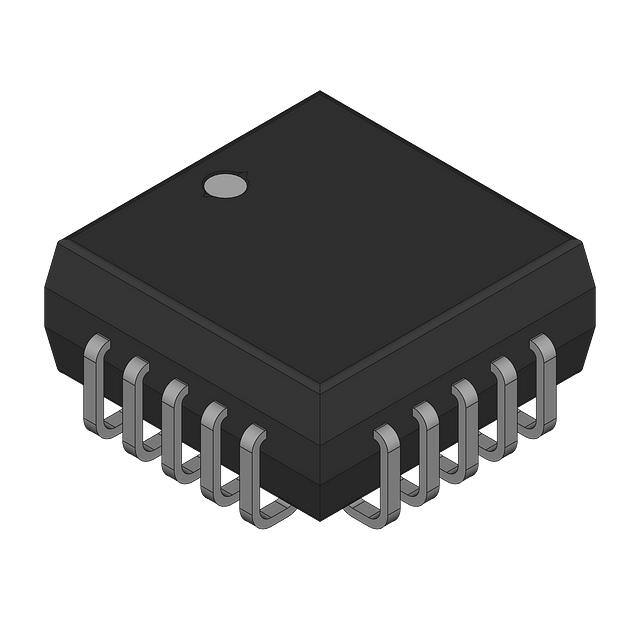
PLCC-20, LCC-20 (TOP VIEW)
Q, L Packages
N/C
B INHIBIT
1
16
A INHIBIT
INV. INPUT
2
15
INHIBIT REF
N.I. INPUT
3
14
VIN
GROUND
4
13
GROUND
GROUND
5
12
GROUND
6
A OUTPUT
11
B INHIBIT
INV INPUT
A INHIBIT
INHIBIT REF
3
B OUTPUT
7
VC
8
10
9
STOP NON-INV.
1
20 19
N.I.INPUT
4
18
VIN
GROUND
5
17
GROUND
N/C
6
16
N/C
GROUND
7
15
GROUND
A OUTPUT
8
14
B OUTPUT
9
FLIP/FLOP
2
10 11 12 13
FLIP/FLOP
STOP INV.
STOP NON-INV.
VC
STOP INV.
N/C
Note: All four ground pins must be connected to a common
ground.
ELECTRICAL CHARACTERISTICS: Unless otherwise stated, these specifications apply for TA = –55°C to +125°C for
the UC1706, –25°C to +85°C for the UC2706 and 0°C to +70°C for the UC3706; VIN = VC = 20V. TA = TJ.
PARAMETERS
TEST CONDITIONS
VIN Supply Current
VIN = 40V
VC Supply Current
VC = 40V, Outputs Low
VC Leakage Current
VIN = 0, VC = 30V, No Load
MIN
TYP
MAX
UNITS
8
10
mA
4
5
mA
.05
0.1
mA
0.8
V
Digital Input Low Level
Digital Input High Level
2.2
V
Input Current
VI = 0
–0.6
–1.0
mA
Input Leakage
VI = 5V
.05
0.1
mA
2
�UC1706
UC2706
UC3706
ELECTRICAL CHARACTERISTICS: Unless otherwise stated, these specifications apply for TA = –55°C to +125°C for
the UC1706, –25°C to +85°C for the UC2706 and 0°C to +70°C for the UC3706; VIN = VC = 20V. TA = TJ.
PARAMETERS
TEST CONDITIONS
MIN
TYP
MAX
UNITS
Output High Sat., VC-VO
IO = -50mA
2.0
V
Output Low Sat., VO
IO = 50mA
0.4
V
IO = 500mA
2.5
V
Inhibit Threshold
VREF = 0.5V
0.4
0.6
V
VREF = 3.5V
3.3
3.7
V
Inhibit Input Current
VREF = 0
Analog Threshold
VCM = 0 to 15V, for the UC2706 and UC3706
100
VCM = 0 to 15V, for the UC1706
80
Input Bias Current
VCM = 0
Thermal Shutdown
–10
–20
µA
130
160
mV
130
160
mV
–10
–20
µA
155
°C
TYPICAL SWITCHING CHARACTERISTICS: VIN = VC = 20V, TA = 25°C. Delays measured to 10% output change.
PARAMETERS
TEST CONDITIONS
OUTPUT CL =
UNITS
open
1.0
2.2
Rise Time Delay
110
130
140
ns
10% to 90% Rise
20
40
60
ns
Fall Time Delay
80
90
110
ns
90% to 10% Fall
25
30
50
ns
120
130
140
ns
From Inv. Input to Output:
nF
From N. I. Input to Output:
Rise Time Delay
10% to 90% Rise
20
40
60
ns
Fall Time Delay
100
120
130
ns
90% to 10% Fall
25
30
50
ns
VC Cross-Conduction Current Spike Duration Output Rise
25
ns
0
ns
Inhibit Delay
Output Fall
Inhibit Ref. = 1V, Inhibit Inv. = 0.5 to 1.5V
250
ns
Analog Shutdown Delay
Stop Non-Inv. = 0V, Stop Inv. = 0 to 0.5V
180
ns
CIRCUIT DESCRIPTION
Outputs
The totem-pole outputs have been designed to minimize
cross-conduction current spikes while maximizing fast,
high-current rise and fall times. Current limiting can be
done externally either at the outputs or at the common
VC pin. The output diodes included have slow recovery
and should be shunted with high-speed external diodes
when driving high-frequency inductive loads.
Flip/Flop
Grounding pin 7 activates the internal flip-flop to alternate the two outputs. With pin 7 open, the two outputs
operate simultaneously and can be paralleled for higher
current operation. Since the flip-flop is triggered by the
digital input, an off-time of at last 200nsec must be provided to allow the flip/flop to change states. Note that the
circuit logic is configured such that the “OFF” state is defined as the outputs low.
Digital Inputs
With both an inverting and non-inverting input available,
either active-high or active-low signals may be accepted.
These are true TTL compatible inputs—the threshold is
approximately 1.2V with no hysteresis; and external pullup resistors are not required.
Inhibit Circuit
Although it may have other uses, this circuit is included to
eliminate the need for deadband control when driving
relatively slow bipolar power transistors. A diode from
each inhibit input to the opposite power switch collector
will keep one output from turning-on until the other has
turned-off. The threshold is determined by the voltage on
pin 15 which can be set from 0.5 to 3.5V. When this circuit is not used, ground pin 15 and leave 1 and 16 open.
3
�UC1706
UC2706
UC3706
CIRCUIT DESCRIPTION (cont.)
use with a 7 to 40V supply; however, with some slight response time degradation, it can also be driven from 5V.
When VIN is low, the entire circuit is disabled and no current is drawn from VC. When combined with a UC1840
PWM, the Driver Bias switch can be used to supply VIN to
the UC1706. VIN switching should be fast as if VC is
high, undefined operation of the outputs may occur with
VIN less than 5V.
Analog Shutdown
This circuit is included to get a latched shutdown as close
to the outputs as possible, from a time standpoint. With
an internal 130mV threshold, this comparator has a
common-mode range from ground to (VIN – 3V). When
not used, both inputs should be grounded. The time required for this circuit to latch is inversely proportional to
the amount of overdrive but reaches a minimum of
180nsec. As with the flip-flop, an input off-time of at least
200nsec is required to reset the latch between pulses.
Thermal Considerations
Should the chip temperature reach approximately 155°C,
a parallel, non--inverting input is activated driving both
outputs to the low state.
Supply Voltage
With an internal 5V regulator, this circuit is optimized for
APPLICATIONS
D1, D2; UC3611 Schottky Diodes
D1, D2; UC3611 Schottky Diodes
Power MOSFET Drive Circuit
Power MOSFET Drive Circuit Using Negative Bias Voltage and
Level Shifting to Ground Referenced PWMs
D1, D2: UC3611 Schottky Diodes
Transformer Coupled MOSFET Drive Circuit
4
Charge Pump Circuits
�UC1706
UC2706
UC3706
APPLICATIONS (cont'd)
D1, D2: UC3611 Schottky Diodes
D1, D2: UC3611 Schottky Diodes
Power Bipolar Drive Circuit
Transformer Coupled Push-Pull MOSFET Drive Circuit
UC3706 Converts Single Output PWMs to High Current Push-Pull Configuration
UNITRODE CORPORATION
7 CONTINENTAL BLVD. • MERRIMACK, NH 03054
TEL. (603) 424-2410 • FAX (603) 424-3460
5
�IMPORTANT NOTICE
Texas Instruments and its subsidiaries (TI) reserve the right to make changes to their products or to discontinue
any product or service without notice, and advise customers to obtain the latest version of relevant information
to verify, before placing orders, that information being relied on is current and complete. All products are sold
subject to the terms and conditions of sale supplied at the time of order acknowledgment, including those
pertaining to warranty, patent infringement, and limitation of liability.
TI warrants performance of its products to the specifications applicable at the time of sale in accordance with
TI’s standard warranty. Testing and other quality control techniques are utilized to the extent TI deems necessary
to support this warranty. Specific testing of all parameters of each device is not necessarily performed, except
those mandated by government requirements.
Customers are responsible for their applications using TI components.
In order to minimize risks associated with the customer’s applications, adequate design and operating
safeguards must be provided by the customer to minimize inherent or procedural hazards.
TI assumes no liability for applications assistance or customer product design. TI does not warrant or represent
that any license, either express or implied, is granted under any patent right, copyright, mask work right, or other
intellectual property right of TI covering or relating to any combination, machine, or process in which such
products or services might be or are used. TI’s publication of information regarding any third party’s products
or services does not constitute TI’s approval, license, warranty or endorsement thereof.
Reproduction of information in TI data books or data sheets is permissible only if reproduction is without
alteration and is accompanied by all associated warranties, conditions, limitations and notices. Representation
or reproduction of this information with alteration voids all warranties provided for an associated TI product or
service, is an unfair and deceptive business practice, and TI is not responsible nor liable for any such use.
Resale of TI’s products or services with statements different from or beyond the parameters stated by TI for
that product or service voids all express and any implied warranties for the associated TI product or service,
is an unfair and deceptive business practice, and TI is not responsible nor liable for any such use.
Also see: Standard Terms and Conditions of Sale for Semiconductor Products. www.ti.com/sc/docs/stdterms.htm
Mailing Address:
Texas Instruments
Post Office Box 655303
Dallas, Texas 75265
Copyright 2001, Texas Instruments Incorporated
�PACKAGE OPTION ADDENDUM
www.ti.com
30-Aug-2005
PACKAGING INFORMATION
Orderable Device
Status (1)
Package
Type
Package
Drawing
Pins Package Eco Plan (2)
Qty
5962-8961101EA
ACTIVE
CDIP
J
16
1
TBD
A42 SNPB
Level-NC-NC-NC
UC1706J
ACTIVE
CDIP
J
16
1
TBD
A42 SNPB
Level-NC-NC-NC
UC1706J/80891
ACTIVE
CDIP
J
16
TBD
Call TI
UC1706J883B
ACTIVE
CDIP
J
16
1
TBD
A42 SNPB
UC1706L
ACTIVE
LCCC
FK
20
1
TBD
UC1706L/81031
ACTIVE
LCCC
FK
20
UC1706L883B
ACTIVE
LCCC
FK
20
1
TBD
UC2706DW
ACTIVE
SOIC
DW
16
40
TBD
CU NIPDAU
Level-1-220C-UNLIM
UC2706DWTR
ACTIVE
SOIC
DW
16
2000
TBD
CU NIPDAU
Level-1-220C-UNLIM
UC2706J
ACTIVE
CDIP
J
16
1
TBD
A42 SNPB
Level-NC-NC-NC
UC2706N
ACTIVE
PDIP
N
16
25
Green (RoHS &
no Sb/Br)
Call TI
Level-NC-NC-NC
UC2706NG4
ACTIVE
PDIP
N
16
25
Green (RoHS &
no Sb/Br)
Call TI
Level-NC-NC-NC
UC2706Q
ACTIVE
PLCC
FN
20
46
TBD
Call TI
Level-2-220C-1 YEAR
UC2706QTR
ACTIVE
PLCC
FN
20
1000
TBD
Call TI
Level-2-220C-1 YEAR
UC3706DW
ACTIVE
SOIC
DW
16
40
TBD
CU NIPDAU
Level-1-220C-UNLIM
UC3706DWTR
ACTIVE
SOIC
DW
16
2000
TBD
CU NIPDAU
Level-1-220C-UNLIM
TBD
Lead/Ball Finish
MSL Peak Temp (3)
Call TI
Level-NC-NC-NC
POST-PLATE Level-NC-NC-NC
Call TI
Call TI
POST-PLATE Level-NC-NC-NC
UC3706J
ACTIVE
CDIP
J
16
1
TBD
A42 SNPB
Level-NC-NC-NC
UC3706N
ACTIVE
PDIP
N
16
25
Green (RoHS &
no Sb/Br)
Call TI
Level-NC-NC-NC
UC3706NG4
ACTIVE
PDIP
N
16
25
Green (RoHS &
no Sb/Br)
Call TI
Level-NC-NC-NC
UC3706Q
ACTIVE
PLCC
FN
20
46
TBD
Call TI
Level-2-220C-1 YEAR
UC3706QTR
ACTIVE
PLCC
FN
20
1000
TBD
Call TI
Level-2-220C-1 YEAR
(1)
The marketing status values are defined as follows:
ACTIVE: Product device recommended for new designs.
LIFEBUY: TI has announced that the device will be discontinued, and a lifetime-buy period is in effect.
NRND: Not recommended for new designs. Device is in production to support existing customers, but TI does not recommend using this part in
a new design.
PREVIEW: Device has been announced but is not in production. Samples may or may not be available.
OBSOLETE: TI has discontinued the production of the device.
(2)
Eco Plan - The planned eco-friendly classification: Pb-Free (RoHS) or Green (RoHS & no Sb/Br) - please check
http://www.ti.com/productcontent for the latest availability information and additional product content details.
TBD: The Pb-Free/Green conversion plan has not been defined.
Pb-Free (RoHS): TI's terms "Lead-Free" or "Pb-Free" mean semiconductor products that are compatible with the current RoHS requirements
for all 6 substances, including the requirement that lead not exceed 0.1% by weight in homogeneous materials. Where designed to be soldered
at high temperatures, TI Pb-Free products are suitable for use in specified lead-free processes.
Green (RoHS & no Sb/Br): TI defines "Green" to mean Pb-Free (RoHS compatible), and free of Bromine (Br) and Antimony (Sb) based flame
retardants (Br or Sb do not exceed 0.1% by weight in homogeneous material)
(3)
MSL, Peak Temp. -- The Moisture Sensitivity Level rating according to the JEDEC industry standard classifications, and peak solder
temperature.
Important Information and Disclaimer:The information provided on this page represents TI's knowledge and belief as of the date that it is
provided. TI bases its knowledge and belief on information provided by third parties, and makes no representation or warranty as to the
accuracy of such information. Efforts are underway to better integrate information from third parties. TI has taken and continues to take
reasonable steps to provide representative and accurate information but may not have conducted destructive testing or chemical analysis on
Addendum-Page 1
�PACKAGE OPTION ADDENDUM
www.ti.com
30-Aug-2005
incoming materials and chemicals. TI and TI suppliers consider certain information to be proprietary, and thus CAS numbers and other limited
information may not be available for release.
In no event shall TI's liability arising out of such information exceed the total purchase price of the TI part(s) at issue in this document sold by TI
to Customer on an annual basis.
Addendum-Page 2
�IMPORTANT NOTICE
Texas Instruments Incorporated and its subsidiaries (TI) reserve the right to make corrections, modifications,
enhancements, improvements, and other changes to its products and services at any time and to discontinue
any product or service without notice. Customers should obtain the latest relevant information before placing
orders and should verify that such information is current and complete. All products are sold subject to TI’s terms
and conditions of sale supplied at the time of order acknowledgment.
TI warrants performance of its hardware products to the specifications applicable at the time of sale in
accordance with TI’s standard warranty. Testing and other quality control techniques are used to the extent TI
deems necessary to support this warranty. Except where mandated by government requirements, testing of all
parameters of each product is not necessarily performed.
TI assumes no liability for applications assistance or customer product design. Customers are responsible for
their products and applications using TI components. To minimize the risks associated with customer products
and applications, customers should provide adequate design and operating safeguards.
TI does not warrant or represent that any license, either express or implied, is granted under any TI patent right,
copyright, mask work right, or other TI intellectual property right relating to any combination, machine, or process
in which TI products or services are used. Information published by TI regarding third-party products or services
does not constitute a license from TI to use such products or services or a warranty or endorsement thereof.
Use of such information may require a license from a third party under the patents or other intellectual property
of the third party, or a license from TI under the patents or other intellectual property of TI.
Reproduction of information in TI data books or data sheets is permissible only if reproduction is without
alteration and is accompanied by all associated warranties, conditions, limitations, and notices. Reproduction
of this information with alteration is an unfair and deceptive business practice. TI is not responsible or liable for
such altered documentation.
Resale of TI products or services with statements different from or beyond the parameters stated by TI for that
product or service voids all express and any implied warranties for the associated TI product or service and
is an unfair and deceptive business practice. TI is not responsible or liable for any such statements.
Following are URLs where you can obtain information on other Texas Instruments products and application
solutions:
Products
Applications
Amplifiers
amplifier.ti.com
Audio
www.ti.com/audio
Data Converters
dataconverter.ti.com
Automotive
www.ti.com/automotive
DSP
dsp.ti.com
Broadband
www.ti.com/broadband
Interface
interface.ti.com
Digital Control
www.ti.com/digitalcontrol
Logic
logic.ti.com
Military
www.ti.com/military
Power Mgmt
power.ti.com
Optical Networking
www.ti.com/opticalnetwork
Microcontrollers
microcontroller.ti.com
Security
www.ti.com/security
Telephony
www.ti.com/telephony
Video & Imaging
www.ti.com/video
Wireless
www.ti.com/wireless
Mailing Address:
Texas Instruments
Post Office Box 655303 Dallas, Texas 75265
Copyright 2005, Texas Instruments Incorporated
�


 工商网监
湘ICP备2023018690号
工商网监
湘ICP备2023018690号
