Product
Folder
Order
Now
Support &
Community
Tools &
Software
Technical
Documents
UCC21225A
SLUSCV6A – APRIL 2017 – REVISED FEBRUARY 2018
UCC21225A 4-A, 6-A, 2.5-kVRMS Isolated Dual-Channel Gate Driver in LGA
1 Features
3 Description
•
The UCC21225A is an isolated dual-channel gate
driver with 4-A source and 6-A sink peak current in a
5-mm x 5-mm LGA-13 package. It is designed to
drive power transistors up to 5-MHz with best-in-class
propagation delay and pulse-width distortion.
1
•
•
•
•
•
•
•
•
•
•
•
Universal: Dual Low-Side, Dual High-Side or HalfBridge Driver
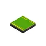
5 x 5 mm, Space-Saving LGA-13 Package
Switching Parameters:
– 19-ns Typical Propagation Delay
– 5-ns Maximum Delay Matching
– 6-ns Maximum Pulse-Width Distortion
CMTI Greater than 100-V/ns
4-A Peak Source, 6-A Peak Sink Output
TTL and CMOS Compatible Inputs
3-V to 18-V Input VCCI Range
Up to 25-V VDD with 5-V UVLO
Programmable Overlap and Dead Time
Rejects Input Transients Shorter than 5-ns
Fast Disable for Power Sequencing
Safety-Related Certifications:
– 3535-VPK Isolation per DIN V VDE V 088411:2017-01
– 2500-VRMS Isolation for 1 Minute per UL 1577
– CQC per GB4943.1-2011 (Planned)
The input side is isolated from the two output drivers
by a 2.5-kVRMS isolation barrier, with 100-V/ns
minimum common-mode transient immunity (CMTI).
Internal functional isolation between the two
secondary side drivers allows working voltage up to
700-VDC.
This driver can be configured as two low-side, two
high-side, or a half-bridge driver with programmable
dead time (DT). A disable pin shuts down both
outputs simultaneously when it is set high, and allows
normal operation when left open or grounded.
The device accepts VDD supply voltages up to 25-V.
A wide input VCCI range from 3-V to 18-V makes the
driver suitable for interfacing with both analog and
digital controllers. All the supply voltage pins have
under voltage lock-out (UVLO) protection.
With all these advanced features, the UCC21225A
enables high power density, high efficiency, and
robustness in a wide variety of power applications.
2 Applications
•
•
•
•
Device Information(1)
Server, Telecom, IT and Industrial Infrastructures
DC-DC and AC-to-DC Power Supplies
Motor Drive and DC-to-AC Solar Inverters
HEV and BEV Battery Chargers
PART NUMBER
UCC21225ANPL
PACKAGE
BODY SIZE (NOM)
NPL LGA (13)
5 mm x 5 mm
(1) For all available packages, see the orderable addendum at
the end of the data sheet.
Functional Block Diagram
VCCI 4,7
13 VDDA
Driver
2
DIS
5
MOD
6
INB
3
GND
1
UVLO
12 OUTA
11 VSSA
Disable,
UVLO
and
Deadtime
DT
DEMOD
Isolation Barrier
INA
Functional Isolation
10 VDDB
Driver
MOD
DEMOD
UVLO
9
OUTB
8
VSSB
Copyright © 2017, Texas Instruments Incorporated
1
An IMPORTANT NOTICE at the end of this data sheet addresses availability, warranty, changes, use in safety-critical applications,
intellectual property matters and other important disclaimers. PRODUCTION DATA.
�UCC21225A
SLUSCV6A – APRIL 2017 – REVISED FEBRUARY 2018
www.ti.com
Table of Contents
1
2
3
4
5
6
Features ..................................................................
Applications ...........................................................
Description .............................................................
Revision History.....................................................
Pin Configuration and Functions .........................
Specifications.........................................................
1
1
1
2
3
4
6.1
6.2
6.3
6.4
6.5
6.6
6.7
6.8
6.9
6.10
6.11
Absolute Maximum Ratings ...................................... 4
ESD Ratings.............................................................. 4
Recommended Operating Conditions....................... 4
Thermal Information .................................................. 5
Power Ratings........................................................... 5
Insulation Specifications............................................ 6
Safety-Related Certifications..................................... 7
Safety-Limiting Values .............................................. 7
Electrical Characteristics........................................... 8
Switching Characteristics ........................................ 9
Insulation Characteristics and Thermal Derating
Curves........................................................................ 9
6.12 Typical Characteristics .......................................... 11
7
Parameter Measurement Information ................ 15
7.1
7.2
7.3
7.4
Propagation Delay and Pulse Width Distortion.......
Rising and Falling Time .........................................
Input and Disable Response Time..........................
Programable Dead Time ........................................
15
15
15
16
7.5 Power-up UVLO Delay to OUTPUT........................ 16
7.6 CMTI Testing........................................................... 17
8
Detailed Description ............................................ 18
8.1
8.2
8.3
8.4
9
Overview .................................................................
Functional Block Diagram .......................................
Feature Description.................................................
Device Functional Modes........................................
18
18
19
23
Application and Implementation ........................ 25
9.1 Application Information............................................ 25
9.2 Typical Application .................................................. 25
10 Power Supply Recommendations ..................... 36
11 Layout................................................................... 37
11.1 Layout Guidelines ................................................. 37
11.2 Layout Example .................................................... 38
12 Device and Documentation Support ................. 40
12.1
12.2
12.3
12.4
12.5
12.6
Documentation Support .......................................
Certifications .........................................................
Community Resources..........................................
Trademarks ...........................................................
Electrostatic Discharge Caution ............................
Glossary ................................................................
40
40
40
40
40
40
13 Mechanical, Packaging, and Orderable
Information ........................................................... 40
4 Revision History
Changes from Original (April 2017) to Revision A
Page
•
Changed the descriptions on feature, application and description sections .......................................................................... 1
•
Changed Safety-Related and Regulatory Approvals to Safety-Related Certifications ........................................................... 1
•
Changed UL and VDE safety-related certification descriptions in features section from planned to completed ................... 1
•
Deleted CSA certification description ..................................................................................................................................... 1
•
Changed detailed description for DISABLE Pin and DT Pin .................................................................................................. 3
•
Changed the testing conditions for the power ratings ........................................................................................................... 5
•
Changed the overvoltage category on the insulation specification section ........................................................................... 6
•
Changed from VDE V 0884-10:2006-12 to VDE V 0884-11:2017-01 in safety-related certifications .................................... 6
•
Changed VIOSM in insulation specifications from 3535VPK to 3500VPK ................................................................................... 6
•
Changed from VDE V 0884-10 to VDE V 0884-11 in insulation specification and safety-related certification table ............ 7
•
Added certification number for VDE and UL in safety-related certification table ................................................................... 7
•
Added 320-VRMS maximum working voltage in the safety-related certification table.............................................................. 7
•
Changed table note to explain how safety-limiting values are calculated ............................................................................. 7
•
Added minimum specifications for propagation delay tPDHL and tPDLH ................................................................................... 9
•
Added CMTI specification to be replaced by |CMH| and |CML|............................................................................................... 9
•
Added feature description for UVLO delay to OUTPUT ...................................................................................................... 16
•
Added footnote on INPUT/OUTPUT logic table .................................................................................................................. 21
•
Added bullet "It is recommended..." bullet to the component placement in the Layout Guidelines section......................... 37
•
Added UL and VDE online certification directory to the certification section ....................................................................... 40
2
Submit Documentation Feedback
Copyright © 2017–2018, Texas Instruments Incorporated
Product Folder Links: UCC21225A
�UCC21225A
www.ti.com
SLUSCV6A – APRIL 2017 – REVISED FEBRUARY 2018
5 Pin Configuration and Functions
NPL Package
13-pin LGA
Top View
GND
1
13
VDDA
INA
2
12
OUTA
INB
3
11
VSSA
VCCI
4
DISABLE
5
10
VDDB
DT
6
9
OUTB
VCCI
7
8
VSSB
Not to scale
Pin Functions
PIN
NAME
DISABLE
NO.
5
I/O (1)
DESCRIPTION
I
Disables both driver outputs if asserted high, enables if set low or left open. This pin is pulled
low internally if left open. It is recommended to tie this pin to ground if not used to achieve
better noise immunity. Bypass using a ≈1nF low ESR/ESL capacitor close to DIS pin when
connecting to a micro controller with distance.
DT
6
I
Programmable dead time function.
Tying DT to VCCI allows the outputs to overlap. Leaving DT open sets the dead time to 21
µm
CTI
Comparative tracking index
DIN EN 60112 (VDE 0303-11); IEC 60112
> 600
V
Material group
Overvoltage category per
IEC 60664-1
I
Rated mains voltage ≤ 150 VRMS
I-III
Rated mains voltage ≤ 300 VRMS
I-II
DIN V VDE V 0884-11 (VDE V 0884-11): 2017-01 (3)
VIORM
Maximum repetitive peak
isolation voltage
VIOWM
Maximum working isolation
voltage
VIOTM
Maximum transient isolation
voltage
VIOSM
Maximum surge isolation
voltage (4)
Apparent charge (5)
qpd
Barrier capacitance, input to
output (6)
CIO
Isolation resistance, input to
output
RIO
AC voltage (bipolar)
792
VPK
AC voltage (sine wave); time dependent dielectric breakdown
(TDDB) test; (See Figure 1)
560
VRMS
DC Voltage
792
VDC
VTEST = VIOTM, t = 60 s (qualification); VTEST = 1.2 × VIOTM, t
= 1 s (100% production)
3535
VPK
Test method per IEC 62368-1, 1.2/50 μs waveform, VTEST =
1.3 × VIOSM (qualification)
3500
VPK
Method a, After Input/Output safety test subgroup 2/3,
Vini = VIOTM, tini = 60s;
Vpd(m) = 1.2 × VIORM, tm = 10s
109
Pollution degree
2
Climatic category
40/125/21
Ω
UL 1577
VISO
(1)
(2)
(3)
(4)
(5)
(6)
6
Withstand isolation voltage
VTEST = VISO = 3000 VRMS, t = 60 sec. (qualification),
VTEST = 1.2 × VISO = 3000VRMS, t = 1 sec (100% production)
2500
VRMS
Creepage and clearance requirements should be applied according to the specific equipment isolation standards of an application. Care
should be taken to maintain the creepage and clearance distance of a board design to ensure that the mounting pads of the isolator on
the printed-circuit board do not reduce this distance. Creepage and clearance on a printed-circuit board become equal in certain cases.
Techniques such as inserting grooves, ribs, or both on a printed circuit board are used to help increase these specifications.
Package dimension tolerance ± 0.05mm.
This coupler is suitable for basic electrical insulation only within the maximum operating ratings. Compliance with the safety ratings shall
be ensured by means of suitable protective circuits.
Testing is carried out in air or oil to determine the intrinsic surge immunity of the isolation barrier.
Apparent charge is electrical discharge caused by a partial discharge (pd).
All pins on each side of the barrier tied together creating a two-pin device.
Submit Documentation Feedback
Copyright © 2017–2018, Texas Instruments Incorporated
Product Folder Links: UCC21225A
�UCC21225A
www.ti.com
SLUSCV6A – APRIL 2017 – REVISED FEBRUARY 2018
6.7 Safety-Related Certifications
VDE
UL
Certified according to DIN V VDE V 0884-11:2017-01
CQC
Recognized under UL 1577
Component Recognition Program
Plan to certify according to GB 4943.12011
Basic Insulation Maximum Transient Overvoltage, 3535 VPK;
Maximum Repetitive Peak Voltage, 792 VPK;
Single protection, 2500 VRMS
Maximum Surge Isolation Voltage, 2719 VPK
Basic Insulation,
Altitude ≤ 5000 m,
Tropical Climate 320-VRMS maximum
working voltage
Certification Number: 40016131
Agency Qualification Planned
Certification Number: E181974
6.8 Safety-Limiting Values
Safety limiting intends to minimize potential damage to the isolation barrier upon failure of input or output circuitry.
PARAMETER
IS
TEST CONDITIONS
Safety output supply
current (1)
RθJA = 98.0ºC/W, VDDA/B = 12 V, TA =
25°C, TJ = 150°C
See Figure 2
RθJA = 98.0ºC/W, VDDA/B = 25 V, TA =
25°C, TJ = 150°C
PS
TS
(1)
Safety supply power (1)
Safety temperature
SIDE
MIN
TYP
MAX
UNIT
DRIVER A,
DRIVER B
50
mA
DRIVER A,
DRIVER B
24
mA
INPUT
0.05
RθJA = 98.0ºC/W, TA = 25°C, TJ = 150°C
DRIVER A
0.60
See Figure 3
DRIVER B
0.60
TOTAL
1.25
(1)
150
W
°C
The maximum safety temperature, TS, has the same value as the maximum junction temperature, TJ, specified for the device. The IS
and PS parameters represent the safety current and safety power respectively. The maximum limits of IS and PS should not be
exceeded. These limits vary with the ambient temperature, TA.
The junction-to-air thermal resistance, RθJA, in the Thermal Information table is that of a device installed on a high-K test board for
leaded surface-mount packages. Use these equations to calculate the value for each parameter:
TJ = TA + RθJA × P, where P is the power dissipated in the device.
TJ(max) = TS = TA + RθJA × PS, where TJ(max) is the maximum allowed junction temperature.
PS = IS × VI, where VI is the maximum input voltage.
Submit Documentation Feedback
Copyright © 2017–2018, Texas Instruments Incorporated
Product Folder Links: UCC21225A
7
�UCC21225A
SLUSCV6A – APRIL 2017 – REVISED FEBRUARY 2018
www.ti.com
6.9 Electrical Characteristics
VVCCI = 3.3 V or 5 V, 0.1-µF capacitor from VCCI to GND, VVDDA = VVDDB = 12 V, 1-µF capacitor from VDDA and VDDB to
VSSA and VSSB, TA = –40°C to +125°C, (unless otherwise noted)
PARAMETER
TEST CONDITIONS
MIN
TYP
MAX
UNIT
SUPPLY CURRENTS
IVCCI
VCCI quiescent current
VINA = 0 V, VINB = 0 V
1.5
2.0
mA
IVDDA,
IVDDB
VDDA and VDDB quiescent current
VINA = 0 V, VINB = 0 V
1.0
1.8
mA
IVCCI
VCCI operating current
(f = 500 kHz) current per channel,
COUT = 100 pF
2.0
mA
IVDDA,
IVDDB
VDDA and VDDB operating current
(f = 500 kHz) current per channel,
COUT = 100 pF
2.5
mA
VCCI SUPPLY UNDERVOLTAGE LOCKOUT THRESHOLDS
VVCCI_ON
Rising threshold VCCI_ON
2.55
2.7
2.85
V
VVCCI_OFF
Falling threshold VCCI_OFF
2.35
2.5
2.65
V
VVCCI_HYS
Threshold hysteresis
0.2
V
VDD SUPPLY UNDERVOLTAGE LOCKOUT THRESHOLDS
VVDDA_ON,
VVDDB_ON
Rising threshold VDDA_ON,
VDDB_ON
5.7
6.0
6.3
V
VVDDA_OFF,
VVDDB_OFF
Falling threshold VDDA_OFF,
VDDB_OFF
5.4
5.7
6
V
VVDDA_HYS,
VVDDB_HYS
Threshold hysteresis
0.3
V
INA, INB AND DISABLE
VINAH, VINBH,
VDISH
Input high voltage
1.6
1.8
2
V
VINAL, VINBL,
VDISL
Input low voltage
0.8
1
1.2
V
VINA_HYS,
VINB_HYS,
VDIS_HYS
Input hysteresis
VINA, VINB
Negative transient, ref to GND, 50
ns pulse
Not production tested, bench test
only
IOA+, IOB+
Peak output source current
CVDD = 10 µF, CLOAD = 0.18 µF, f
= 1 kHz, bench measurement
4
A
IOA-, IOB-
Peak output sink current
CVDD = 10 µF, CLOAD = 0.18 µF, f
= 1 kHz, bench measurement
6
A
ROHA, ROHB
Output resistance at high state
IOUT = –10 mA, TA = 25°C, ROHA,
ROHB do not represent drive pullup performance. See tRISE in
Switching Characteristics and
Output Stage for details.
5
Ω
ROLA, ROLB
Output resistance at low state
IOUT = 10 mA, TA = 25°C
0.55
Ω
VOHA, VOHB
Output voltage at high state
VVDDA, VVDDB = 12 V, IOUT = –10
mA, TA = 25°C
11.95
V
VOLA, VOLB
Output voltage at low state
VVDDA, VVDDB = 12 V, IOUT = 10
mA, TA = 25°C
0.8
V
–5
V
OUTPUT
5.5
mV
DEADTIME AND OVERLAP PROGRAMMING
Pull DT pin to VCCI
Dead time
DT pin is left open, min spec
characterized only, tested for
outliers
RDT = 20 kΩ
8
Submit Documentation Feedback
Overlap determined by INA INB
0
160
-
8
15
ns
200
240
ns
Copyright © 2017–2018, Texas Instruments Incorporated
Product Folder Links: UCC21225A
�UCC21225A
www.ti.com
SLUSCV6A – APRIL 2017 – REVISED FEBRUARY 2018
6.10 Switching Characteristics
VVCCI = 3.3 V or 5 V, 0.1-µF capacitor from VCCI to GND, VVDDA = VVDDB = 12 V, 1-µF capacitor from VDDA and VDDB to
VSSA and VSSB, TA = –40°C to +125°C, (unless otherwise noted).
PARAMETER
TEST CONDITIONS
MIN
TYP
MAX
6
16
ns
7
12
ns
20
ns
19
30
ns
19
30
ns
Pulse width distortion |tPDLH – tPDHL|
6
ns
Propagation delays matching
between VOUTA, VOUTB
5
ns
tRISE
Output rise time, 20% to 80%
measured points
COUT = 1.8 nF
tFALL
Output fall time, 90% to 10%
measured points
COUT = 1.8 nF
tPWmin
Minimum pulse width
tPDHL
Propagation delay from INx to OUTx
falling edges
14
tPDLH
Propagation delay from INx to OUTx
rising edges
14
tPWD
tDM
|CMH|
High-level common-mode transient
immunity
INA and INB both are tied to VCCI;
VCM=1200V; (See CMTI Testing)
100
|CML|
Low-level common-mode transient
immunity
INA and INB both are tied to GND;
VCM=1200V; (See CMTI Testing)
100
Output off for less than minimum,
COUT = 0 pF
UNIT
V/ns
6.11 Insulation Characteristics and Thermal Derating Curves
1.E+10
Safety Margin Zone: 672 VRMS, 26 Years
Operating Zone: 560 VRMS, 20 Years
1.E+9
1.E+8
Life Time (sec)
1.E+7
1.E+6
1.E+5
1.E+4
1.E+3
1.E+2
1.E+1
20%
1.E+0
0
500
1000
1500
2000
2500
Stress Voltage (VRMS)
3000
3500
Figure 1. Isolation Capacitor Life Time Projection
Submit Documentation Feedback
Copyright © 2017–2018, Texas Instruments Incorporated
Product Folder Links: UCC21225A
9
�UCC21225A
SLUSCV6A – APRIL 2017 – REVISED FEBRUARY 2018
www.ti.com
1500
60
VDD = 12V
VDD = 25V
50
Safety Limiting Power (mW)
Safety Limiting Current per Channel (mA)
Insulation Characteristics and Thermal Derating Curves (continued)
40
30
20
10
1250
1000
750
500
250
0
0
0
50
100
150
Ambient Temperature (°C)
200
0
D002
Figure 2. Thermal Derating Curve for
Safety-Related Limiting Current
(Current in Each Channel with
Both Channels Running Simultaneously)
10
Submit Documentation Feedback
50
100
150
Ambient Temperature (°C)
200
D003
Figure 3. Thermal Derating Curve for
Safety-Related Limiting Power
Copyright © 2017–2018, Texas Instruments Incorporated
Product Folder Links: UCC21225A
�UCC21225A
www.ti.com
SLUSCV6A – APRIL 2017 – REVISED FEBRUARY 2018
6.12 Typical Characteristics
20
50
16
40
Current (mA)
Current (mA)
VDDA = VDDB = 12 V, VCCI = 3.3 V, TA = 25°C, No load unless otherwise noted.
12
8
4
30
20
10
VDD=12v
VDD=25v
VDD= 12V
VDD= 25V
0
0
0
800
1600
2400
3200
Frequency (kHz)
4000
4800
5600
0
Figure 4. Per Channel Current Consumption vs. Frequency
(No Load, VDD = 12 V or 25 V)
1000
1500
2000
Frequency (kHz)
2500
3000
D001
Figure 5. Per Channel Current Consumption (IVDDA/B) vs.
Frequency (1-nF Load, VDD = 12 V or 25 V)
6
30
50kHz
250kHz
500kHz
1MHz
5
VDD Current (mA)
24
Current (mA)
500
D001
18
12
6
4
3
2
1
VDD= 12V
VDD= 25V
0
10
25
40
55
70
Frequency (kHz)
85
0
-40
100
Figure 6. Per Channel Current Consumption (IVDDA/B) vs.
Frequency (10-nF Load, VDD = 12 V or 25 V)
0
20
2
2
1.6
1.8
1.2
0.8
0.4
40
60
80 100
Temperature (qC)
140
160
D001
1.6
1.4
1.2
VDD= 12V
VDD= 25V
0
-40
120
Figure 7. Per Channel (IVDDA/B) Supply Current Vs.
Temperature (No Load, Different Switching Frequencies)
Current (mA)
Current (mA)
-20
D001
-20
0
20
40
60
80
Temperature (qC)
100
120
VCCI= 3.3V
VCCI= 5V
140
1
-40
-20
D001
Figure 8. Per Channel (IVDDA/B) Quiescent Supply Current vs
Temperature (No Load, Input Low, No Switching)
0
20
40
60
80
Temperature (qC)
100
120
140
D001
Figure 9. IVCCI Quiescent Supply Current vs Temperature
(No Load, Input Low, No Switching)
Submit Documentation Feedback
Copyright © 2017–2018, Texas Instruments Incorporated
Product Folder Links: UCC21225A
11
�UCC21225A
SLUSCV6A – APRIL 2017 – REVISED FEBRUARY 2018
www.ti.com
Typical Characteristics (continued)
25
10
20
8
Resistance (:)
Time (ns)
VDDA = VDDB = 12 V, VCCI = 3.3 V, TA = 25°C, No load unless otherwise noted.
15
10
5
6
Output Pull-Up
Output Pull-Down
4
2
tRISE
tFALL
0
0
2
4
6
8
0
-40
10
Load (nF)
Figure 10. Rising and Falling Times vs. Load (VDD = 12 V)
0
28
20
24
19
20
16
20
40
60
80
Temperature (qC)
12
140
D001
17
16
8
-40
Rising Edge (tPDLH)
Falling Edge (tPDHL)
15
-20
0
20
40
60
80
Temperature (qC)
100
120
140
3
6
9
12
15
VCCI (V)
D001
Figure 12. Propagation Delay vs. Temperature
18
D001
Figure 13. Propagation Delay vs. VCCI
5
5
Propagation Delay Matching (ns)
Pulse Width Distortion (ns)
120
18
Rising Edge (tPDLH)
Falling Edge (tPDHL)
3
1
-1
-3
-5
-40
-20
0
20
40
60
80
Temperature (qC)
100
120
140
2.5
0
-2.5
Rising Edge
Falling Edge
-5
10
D001
Figure 14. Pulse Width Distortion vs. Temperature
12
100
Figure 11. Output Resistance vs. Temperature
Propagation Delay (ns)
Propagation Delay (ns)
-20
D001
13
16
19
VDDA/B (V)
22
25
D001
Figure 15. Propagation Delay Matching (tDM) vs. VDD
Submit Documentation Feedback
Copyright © 2017–2018, Texas Instruments Incorporated
Product Folder Links: UCC21225A
�UCC21225A
www.ti.com
SLUSCV6A – APRIL 2017 – REVISED FEBRUARY 2018
Typical Characteristics (continued)
VDDA = VDDB = 12 V, VCCI = 3.3 V, TA = 25°C, No load unless otherwise noted.
350
330
2.5
Hysteresis (mV)
Propagation Delay Matching (ns)
5
0
310
290
-2.5
270
Rising Edge
Falling Edge
-5
-40
-20
0
20
40
60
80
Temperature (qC)
100
120
250
-40
140
Figure 16. Propagation Delay Matching (tDM) vs.
Temperature
0
20
40
60
80
Temperature (qC)
100
140
D001
900
IN/DIS Hysteresis (mV)
6
5.5
850
800
750
VCC=3.3V
VCC=5V
VCC=12V
VVDD_ON
VVDD_OFF
5
-40
-20
0
20
40
60
80
Temperature (qC)
100
120
700
-40
140
1.14
1.92
IN/DIS High Threshold (V)
2
1.08
1.02
0.96
VCC=3.3V
VCC= 5V
VCC=12V
-20
0
20
40
60
80
Temperature (qC)
0
100
120
140
20
40
60
80
Temperature (°C)
100
120
140
D001
Figure 19. IN/DIS Hysteresis vs. Temperature
1.2
0.9
-40
-20
D001
Figure 18. VDD UVLO Threshold vs. Temperature
IN/DIS Low Threshold (V)
120
Figure 17. VDD UVLO Hysteresis vs. Temperature
6.5
UVLO Threshold (V)
-20
D001
1.84
1.76
1.68
1.6
-40
VCC=3.3V
VCC= 5V
VCC=12V
-20
D001
Figure 20. IN/DIS Low Threshold
0
20
40
60
80
Temperature (qC)
100
120
Product Folder Links: UCC21225A
D001
Figure 21. IN/DIS High Threshold
Submit Documentation Feedback
Copyright © 2017–2018, Texas Instruments Incorporated
140
13
�UCC21225A
SLUSCV6A – APRIL 2017 – REVISED FEBRUARY 2018
www.ti.com
Typical Characteristics (continued)
VDDA = VDDB = 12 V, VCCI = 3.3 V, TA = 25°C, No load unless otherwise noted.
5
1500
1200
-6
900
-17
'DT (ns)
Dead Time (ns)
RDT= 20k:
RDT= 100k:
600
-28
-39
300
RDT= 20k:
RDT = 100k:
0
-40
-20
0
20
40
60
80
Temperature (qC)
100
120
140
-20
D001
Figure 22. Dead Time vs. Temperature (with RDT = 20 kΩ and
100 kΩ)
14
-50
-40
0
20
40
60
80
Temperature (qC)
100
120
140
D001
Figure 23. Dead Time Matching vs. Temperature (with RDT =
20 kΩ and 100 kΩ)
Submit Documentation Feedback
Copyright © 2017–2018, Texas Instruments Incorporated
Product Folder Links: UCC21225A
�UCC21225A
www.ti.com
SLUSCV6A – APRIL 2017 – REVISED FEBRUARY 2018
7 Parameter Measurement Information
7.1 Propagation Delay and Pulse Width Distortion
Figure 24 shows how to calculate pulse width distortion (tPWD) and delay matching (tDM) from the propagation
delays of channels A and B. These parameters can be measured by ensuring that both inputs are in phase and
disabling the dead time function by shorting the DT Pin to VCC.
INA/B
tPDHLA
tPDLHA
tDM
OUTA
tPDLHB
tPDHLB
tPWDB = |tPDLHB t tPDHLB|
OUTB
Figure 24. Overlapping Inputs, Dead Time Disabled
7.2 Rising and Falling Time
Figure 25 shows the criteria for measuring rising (tRISE) and falling (tFALL) times. For more information on how
short rising and falling times are achieved see Output Stage.
80%
tRISE
90%
tFALL
20%
10%
Figure 25. Rising and Falling Time Criteria
7.3 Input and Disable Response Time
Figure 26 shows the response time of the disable function. For more information, see Disable Pin.
INA
DIS High
Response Time
DIS
DIS Low
Response Time
OUTA
90%
90%
tPDLH
tPDHL
10%
10%
10%
Figure 26. Disable Pin Timing
Submit Documentation Feedback
Copyright © 2017–2018, Texas Instruments Incorporated
Product Folder Links: UCC21225A
15
�UCC21225A
SLUSCV6A – APRIL 2017 – REVISED FEBRUARY 2018
www.ti.com
7.4 Programable Dead Time
Leaving the DT pin open or tying it to GND through an appropriate resistor (RDT) sets a dead-time interval. For
more details on dead time, refer to Programmable Dead Time (DT) Pin.
INA
INB
90%
OUTA
10%
tPDHL
tPDLH
90%
OUTB
10%
tPDHL
Dead Time
(Set by RDT)
Dead Time
(Determined by Input signals if
longer than DT set by RDT)
Figure 27. Dead-Time Switching Parameters
7.5 Power-up UVLO Delay to OUTPUT
Before the driver is ready to deliver a proper output state, there is a power-up delay from the UVLO rising edge
to output and it is defined as tVCCI+ to OUT for VCCI UVLO (typically 40-µs) and tVDD+ to OUT for VDD UVLO (typically
50-µs). It is recommended to consider proper margin before launching PWM signal after the driver's VCCI and
VDD bias supply is ready. Figure 28 and Figure 29 show the power-up UVLO delay timing diagram for VCCI and
VDD.
If INA or INB are active before VCCI or VDD have crossed above their respective on thresholds, the output will
not update until tVCCI+ to OUT or tVDD+ to OUT after VCCI or VDD crossing its UVLO rising threshold. However, when
either VCCI or VDD receive a voltage less than their respective off thresholds, there is 50µs by the UVLO protection feature.
(For more information on UVLO see VDD, VCCI, and Under Voltage Lock Out (UVLO)). The upper end of the
VDDA/VDDB range depends on the maximum gate voltage of the power device being driven by UCC21225A,
and should not exceed the recommended maximum VDDA/VDDB of 25-V.
A local bypass capacitor should be placed between the VDD and VSS pins, with a value of between 220 nF and
10 µF for device biasing. It is further suggested that an additional 100-nF capacitor be placed in parallel with the
device biasing capacitor for high frequency filtering. Both capacitors should be positioned as close to the device
as possible. Low ESR, ceramic surface mount capacitors are recommended.
Similarly, a bypass capacitor should also be placed between the VCCI and GND pins. Given the small amount of
current drawn by the logic circuitry within the input side of UCC21225A, this bypass capacitor has a minimum
recommended value of 100 nF.
36
Submit Documentation Feedback
Copyright © 2017–2018, Texas Instruments Incorporated
Product Folder Links: UCC21225A
�UCC21225A
www.ti.com
SLUSCV6A – APRIL 2017 – REVISED FEBRUARY 2018
11 Layout
11.1 Layout Guidelines
Designers must pay close attention to PCB layout in order to achieve optimum performance for the UCC21225A.
Below are some key points.
Component Placement:
• Low-ESR and low-ESL capacitors must be connected close to the device between the VCCI and GND pins
and between the VDD and VSS pins to bypass noise and to support high peak currents when turning on the
external power transistor.
• To avoid large negative transients on VSS pins connected to the switch node, the parasitic inductances
between the source of the top transistor and the source of the bottom transistor must be minimized.
• It is recommended to place the dead time setting resistor, RDT, and its bypassing capacitor close to DT pin of
UCC21225A.
• It is recommended to bypass using a ≈1nF low ESR/ESL capacitor, CDIS, close to DIS pin when connecting to
a µC with distance.
Grounding Considerations:
• It is essential to confine the high peak currents that charge and discharge the transistor gates to a minimal
physical area. This will decrease the loop inductance and minimize noise on the gate terminals of the
transistors. The gate driver must be placed as close as possible to the transistors.
• Pay attention to high current path that includes the bootstrap capacitor, bootstrap diode, local VSSBreferenced bypass capacitor, and the low-side transistor body/anti-parallel diode. The bootstrap capacitor is
recharged on a cycle-by-cycle basis through the bootstrap diode by the VDD bypass capacitor. This
recharging occurs in a short time interval and involves a high peak current. Minimizing this loop length and
area on the circuit board is important for ensuring reliable operation.
High-Voltage Considerations:
• To ensure isolation performance between the primary and secondary side, one should avoid placing any PCB
traces or copper below the driver device. PCB cutting or scoring beneath the IC are not recommended, since
this can severely exacerbate board warping and twisting issues.
• For half-bridge, or high-side/low-side configurations, where the channel A and channel B drivers could
operate with a DC-link voltage up to 700 VDC, one should try to increase the creepage distance of the PCB
layout between the high and low-side PCB traces.
Thermal Considerations:
• A large amount of power may be dissipated by the UCC21225A if the driving voltage is high, the load is
heavy, or the switching frequency is high (Refer to Estimate Gate Driver Power Loss for more details). Proper
PCB layout can help dissipate heat from the device to the PCB and minimize junction to board thermal
impedance (θJB).
• Increasing the PCB copper connecting to VDDA, VDDB, VSSA and VSSB pins is recommended, with priority
on maximizing the connection to VSSA and VSSB (see Figure 42 and Figure 43). However, high voltage PCB
considerations mentioned above must be maintained.
• If there are multiple layers in the system, it is also recommended to connect the VDDA, VDDB, VSSA and
VSSB pins to internal ground or power planes through multiple vias of adequate size. These vias should be
located close to the IC pins to maximize thermal conductivity. However, keep in mind that there shouldn’t be
any traces/coppers from different high voltage planes overlapping.
Submit Documentation Feedback
Copyright © 2017–2018, Texas Instruments Incorporated
Product Folder Links: UCC21225A
37
�UCC21225A
SLUSCV6A – APRIL 2017 – REVISED FEBRUARY 2018
www.ti.com
11.2 Layout Example
Figure 41 shows a 2-layer PCB layout example with the signals and key components labeled.
Figure 41. Layout Example
Figure 42 and Figure 43 shows top and bottom layer traces and copper.
NOTE
There are no PCB traces or copper between the primary and secondary side, which
ensures isolation performance.
38
Submit Documentation Feedback
Copyright © 2017–2018, Texas Instruments Incorporated
Product Folder Links: UCC21225A
�UCC21225A
www.ti.com
SLUSCV6A – APRIL 2017 – REVISED FEBRUARY 2018
Layout Example (continued)
PCB trace spacing between the high-side and low-side gate drivers in the output stage are increased to minimize
cross-talk due to parasitic capacitance coupling between the switching node VSSA (SW), where high dv/dt may
exist, and the low-side gate drive circuit.
Figure 42. Top Layer Traces and Copper
Figure 43. Bottom Layer Traces and Copper
Figure 44 and Figure 45 are 3D layout pictures with top view and bottom views.
NOTE
The location of the PCB cutout between the primary side and secondary sides, which
ensures isolation performance.
Figure 44. 3-D PCB Top View
Figure 45. 3-D PCB Bottom View
Submit Documentation Feedback
Copyright © 2017–2018, Texas Instruments Incorporated
Product Folder Links: UCC21225A
39
�UCC21225A
SLUSCV6A – APRIL 2017 – REVISED FEBRUARY 2018
www.ti.com
12 Device and Documentation Support
12.1 Documentation Support
12.1.1 Related Documentation
For related documentation see the following:
• Isolation Glossary
12.2 Certifications
UL Online Certifications Directory, "FPPT2.E181974 Nonoptical Isolating Devices - Component" Certificate
Number: 20170718-E181974,
VDE Pruf- und Zertifizierungsinstitut Certification, Certificate of Conformity with Factory Surveillance
12.2.1 Receiving Notification of Documentation Updates
To receive notification of documentation updates, navigate to the device product folder on ti.com. In the upper
right corner, click on Alert me to register and receive a weekly digest of any product information that has
changed. For change details, review the revision history included in any revised document.
12.3 Community Resources
The following links connect to TI community resources. Linked contents are provided "AS IS" by the respective
contributors. They do not constitute TI specifications and do not necessarily reflect TI's views; see TI's Terms of
Use.
TI E2E™ Online Community TI's Engineer-to-Engineer (E2E) Community. Created to foster collaboration
among engineers. At e2e.ti.com, you can ask questions, share knowledge, explore ideas and help
solve problems with fellow engineers.
Design Support TI's Design Support Quickly find helpful E2E forums along with design support tools and
contact information for technical support.
12.4 Trademarks
E2E is a trademark of Texas Instruments.
12.5 Electrostatic Discharge Caution
These devices have limited built-in ESD protection. The leads should be shorted together or the device placed in conductive foam
during storage or handling to prevent electrostatic damage to the MOS gates.
12.6 Glossary
SLYZ022 — TI Glossary.
This glossary lists and explains terms, acronyms, and definitions.
13 Mechanical, Packaging, and Orderable Information
The following pages include mechanical, packaging, and orderable information. This information is the most
current data available for the designated devices. This data is subject to change without notice and revision of
this document. For browser-based versions of this data sheet, refer to the left-hand navigation.
40
Submit Documentation Feedback
Copyright © 2017–2018, Texas Instruments Incorporated
Product Folder Links: UCC21225A
�PACKAGE OPTION ADDENDUM
www.ti.com
7-Feb-2018
PACKAGING INFORMATION
Orderable Device
Status
(1)
Package Type Package Pins Package
Drawing
Qty
Eco Plan
Lead/Ball Finish
MSL Peak Temp
(2)
(6)
(3)
Op Temp (°C)
Device Marking
(4/5)
UCC21225ANPLR
ACTIVE
VLGA
NPL
13
3000
Green (RoHS
& no Sb/Br)
NIAU
Level-3-260C-168 HR
-40 to 125
UCC21225A
UCC21225ANPLT
ACTIVE
VLGA
NPL
13
250
Green (RoHS
& no Sb/Br)
NIAU
Level-3-260C-168 HR
-40 to 125
UCC21225A
(1)
The marketing status values are defined as follows:
ACTIVE: Product device recommended for new designs.
LIFEBUY: TI has announced that the device will be discontinued, and a lifetime-buy period is in effect.
NRND: Not recommended for new designs. Device is in production to support existing customers, but TI does not recommend using this part in a new design.
PREVIEW: Device has been announced but is not in production. Samples may or may not be available.
OBSOLETE: TI has discontinued the production of the device.
(2)
RoHS: TI defines "RoHS" to mean semiconductor products that are compliant with the current EU RoHS requirements for all 10 RoHS substances, including the requirement that RoHS substance
do not exceed 0.1% by weight in homogeneous materials. Where designed to be soldered at high temperatures, "RoHS" products are suitable for use in specified lead-free processes. TI may
reference these types of products as "Pb-Free".
RoHS Exempt: TI defines "RoHS Exempt" to mean products that contain lead but are compliant with EU RoHS pursuant to a specific EU RoHS exemption.
Green: TI defines "Green" to mean the content of Chlorine (Cl) and Bromine (Br) based flame retardants meet JS709B low halogen requirements of


 工商网监
湘ICP备2023018690号
工商网监
湘ICP备2023018690号
