Product
Folder
Sample &
Buy
Support &
Community
Tools &
Software
Technical
Documents
UCC21521
ZHCSFM4 – OCTOBER 2016
UCC21521 具有使能功能的 4A/6A、
、5.7 kVRMS 隔离式双通道栅极驱动器
1 特性
•
•
•
1
•
•
•
•
•
•
•
•
•
•
•
•
通用:双路低侧、双路高侧或半桥驱动器
工作温度范围:–40°C 至 +125°C
开关参数:
– 19ns 典型传播延迟
– 10ns 最小脉冲宽度
– 5ns 最大延迟匹配度
– 5ns 最大脉宽失真度
共模瞬态抗扰度 (CMTI) 大于 100 V/ns
浪涌抗扰度高达 12.8kV
隔离栅寿命 > 40 年
4A 峰值拉电流,6A 峰值灌电流输出
TTL 和 CMOS 兼容输入
3V 至 18V 输入 VCCI 范围,可连接数字和模拟控
制器
高达 25V 的 VDD 输出驱动电源
– 5V、8V、12V VDD UVLO 选项
可通过编程的重叠和死区时间
抑制短于 5ns 的输入脉冲和瞬态噪声
可针对电源排序快速使能
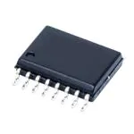
宽体小外形尺寸集成电路 (SOIC)-16 (DW) 封装
安全相关及管理批准:
– 8000 VPK 隔离,符合 DIN V VDE V 0884-10
(VDE V0884-10):2006-12 标准
– 符合 UL 1577 标准且长达 1 分钟的 5700 VRMS
隔离
– CSA 组件验收通知 5A,IEC 60950-1 和 IEC
60601-1 终端设备标准(计划)
– 通过 GB4943.1-2011 CQC 认证(计划)
3 说明
UCC21521 是一款隔离式双通道栅极驱动器,具有 4A
峰值拉电流和 6A 峰值灌电流。该器件设计用于驱动高
达 5MHz 的功率 MOSFET、IGBT 和 SiC MOSFET,
具有一流的传播延迟和脉宽失真度。
输入侧通过一个 5.7 kVRMS 增强型隔离栅与两个输出
驱动器隔离,共模瞬态抗扰度 (CMTI) 的最小值为
100V/ns。两个二次侧驱动器之间采用内部功能隔离,
支持高达 1500 VDC 的工作电压。
该驱动器可配置为两个低侧驱动器、两个高侧驱动器或
一个死区时间 (DT) 可编程的半桥驱动器。EN 引脚拉
低时会同时关闭两个输出,悬空或拉高时可使器件恢复
正常运行。作为一种故障安全机制,一次侧逻辑故障会
强制两个输出为低电平。
此器件接受高达 25V 的 VDD 电源电压。3V 到 18V 的
宽输入电压 VCCI 范围使得该驱动器适用于连接数字和
模拟控制器。所有电源电压引脚均具有欠压闭锁
(UVLO) 保护。
凭借上述所有高级 特性,UCC21521 能够满足各类电
源应用中对于高效率、高电源密度和稳健性的 要求。
器件信息(1)
器件型号
封装
封装尺寸(标称值)
UCC21521ADW
DW SOIC (16)
10.30mm x 7.50mm
UCC21521DW
DW SOIC (16)
10.30mm x 7.50mm
UCC21521CDW
DW SOIC (16)
10.30mm x 7.50mm
(1) 要了解所有可用封装,请见数据表末尾的可订购产品附录。
功能框图
2 应用
离线交流-直流电源中的隔离式转换器
服务器、电信、IT 和工业基础设施
电机驱动和直流-交流太阳能逆变器
LED 照明
感应加热
不间断电源 (UPS)
HEV 和 BEV 电池充电器
VCCI 3,8
16 VDDA
Driver
INA
1
EN
5
NC
7
DT
6
MOD
DEMOD
Reinforced Isolation
•
•
•
•
•
•
•
EN,
UVLO
and
Deadtime
UVLO
15 OUTA
14 VSSA
13 NC
Functional Isolation
12 NC
11 VDDB
Driver
INB
2
GND
4
MOD
DEMOD
UVLO
10 OUTB
9
VSSB
Copyright © 2016, Texas Instruments Incorporated
1
An IMPORTANT NOTICE at the end of this data sheet addresses availability, warranty, changes, use in safety-critical applications,
intellectual property matters and other important disclaimers. PRODUCTION DATA.
English Data Sheet: SLUSCO3
�UCC21521
ZHCSFM4 – OCTOBER 2016
www.ti.com.cn
目录
1
2
3
4
5
6
特性 ..........................................................................
应用 ..........................................................................
说明 ..........................................................................
修订历史...................................................................
Pin Configuration and Functions .........................
Specifications.........................................................
6.1
6.2
6.3
6.4
6.5
6.6
6.7
6.8
6.9
6.10
6.11
6.12
7
7.5 CMTI Testing........................................................... 17
1
1
1
2
3
4
8
8.1
8.2
8.3
8.4
9
Absolute Maximum Ratings ...................................... 4
ESD Ratings.............................................................. 4
Recommended Operating Conditions....................... 4
Thermal Information .................................................. 5
Power Ratings........................................................... 5
Insulation Specifications............................................ 6
Safety-Related Certifications..................................... 7
Safety-Limiting Values .............................................. 7
Electrical Characteristics........................................... 8
Switching Characteristics ........................................ 9
Insulation Characteristics Curves ......................... 10
Typical Characteristics .......................................... 11
Propagation Delay and Pulse Width Distortion.......
Rising and Falling Time .........................................
Input and Enable Response Time...........................
Programable Dead Time ........................................
Overview .................................................................
Functional Block Diagram .......................................
Feature Description.................................................
Device Functional Modes........................................
18
18
19
23
Application and Implementation ........................ 25
9.1 Application Information............................................ 25
9.2 Typical Application .................................................. 25
10 Power Supply Recommendations ..................... 36
11 Layout................................................................... 37
11.1 Layout Guidelines ................................................. 37
11.2 Layout Example .................................................... 38
12 器件和文档支持 ..................................................... 40
12.1
12.2
12.3
12.4
12.5
12.6
12.7
Parameter Measurement Information ................ 16
7.1
7.2
7.3
7.4
Detailed Description ............................................ 18
16
16
16
17
文档支持 ...............................................................
认证 .......................................................................
接收文档更新通知 .................................................
社区资源................................................................
商标 .......................................................................
静电放电警告.........................................................
Glossary ................................................................
40
40
40
40
40
40
40
13 机械、封装和可订购信息 ....................................... 40
4 修订历史
2
日期
修订版本
注释
2016 年 10 月
*
最初发布版本
Copyright © 2016, Texas Instruments Incorporated
�UCC21521
www.ti.com.cn
ZHCSFM4 – OCTOBER 2016
5 Pin Configuration and Functions
DW Package
16-Pin SOIC
Top View
INA
1
16
VDDA
INB
2
15
OUTA
VCCI
3
14
VSSA
GND
4
13
NC
EN
5
12
NC
DT
6
11
VDDB
NC
7
10
OUTB
VCCI
8
9
VSSB
Not to scale
Pin Functions
PIN
NAME
NO.
I/O (1)
DESCRIPTION
Programmable dead time function.
Tying DT to VCCI allows the outputs to overlap. Leaving DT open sets the dead time to 8
mm
Shortest terminal to terminal distance across the package
surface
>8
mm
>21
µm
> 600
V
CLR
External clearance (1)
CPG
External creepage
(1)
DTI
Distance through insulation
Distance through internal isolation (internal clearance)
CTI
Comparative tracking index
DIN EN 60112 (VDE 0303-11); IEC 60112
Material group
According to IEC 60664-1
Overvoltage category per
IEC 60664-1
Rated mains voltage ≤ 600 VRMS
I-IV
Rated mains voltage ≤ 1000 VRMS
I-III
I
DIN V VDE 0884-10 (VDE V 0884-10): 2006-2012 (2)
VIORM
Maximum repetitive peak
isolation voltage
AC voltage (bipolar)
VIOWM
Maximum isolation working
voltage
Time dependent dielectric breakdown (TDDB) test, (See 图 1)
VIOTM
Maximum transient isolation
voltage
VIOSM
Maximum surge isolation
voltage (3)
2121
VPK
1500
VRMS
2121
VDC
VTEST = VIOTM
t = 60 sec (qualification)
t = 1 sec (100% production)
8000
VPK
Test method per IEC 60065, 1.2/50 µs waveform, VTEST = 1.6
× VIOSM = 12800 VPK (qualification)
8000
VPK
Method a, After Input/Output safety test subgroup 2/3. Vini =
VIOTM, tini = 60s;
109
Pollution degree
2
Climatic category
40/125/21
pF
Ω
UL 1577
VISO
(1)
(2)
(3)
(4)
(5)
6
Withstand isolation voltage
VTEST = VISO = 5700 VRMS, t = 60 sec. (qualification),
VTEST = 1.2 × VISO = 6840VRMS, t = 1 sec (100% production)
5700
VRMS
Creepage and clearance requirements should be applied according to the specific equipment isolation standards of an application. Care
should be taken to maintain the creepage and clearance distance of a board design to ensure that the mounting pads of the isolator on
the printed-circuit board do not reduce this distance. Creepage and clearance on a printed-circuit board become equal in certain cases.
Techniques such as inserting grooves and/or ribs on a printed circuit board are used to help increase these specifications.
This coupler is suitable for basic electrical insulation only within the maximum operating ratings. Compliance with the safety ratings shall
be ensured by means of suitable protective circuits.
Testing is carried out in air or oil to determine the intrinsic surge immunity of the isolation barrier.
Apparent charge is electrical discharge caused by a partial discharge (pd).
All pins on each side of the barrier tied together creating a two-terminal device.
Copyright © 2016, Texas Instruments Incorporated
�UCC21521
www.ti.com.cn
ZHCSFM4 – OCTOBER 2016
6.7 Safety-Related Certifications
VDE
CSA
Certified according to
DIN VDE V 0884-10
(VDE V 0884-10):200612 and DIN EN 60950-1
(VDE 0805 Teil 1):201101
Approved under CSA Component
Acceptance Notice 5A, IEC 60950-1 and
IEC 60601-1
UL
CQC
Certified according to UL
1577 Component
Recognition Program
Certified according to GB 4943.12011
Reinforced Insulation
Maximum Transient
Isolation voltage, 8000
VPK; Maximum Repetitive Reinforced insulation per CSA 60950-107+A1+A2 and IEC 60950-1 2nd Ed.
Peak Isolation Voltage,
2121 VPK; Maximum
Surge Isolation Voltage,
8000 VPK
Single protection, 5700 VRMS
Reinforced Insulation,
Altitude ≤ 5000 m,
Tropical Climate
Certification number:
40040142
File number: E181974
Agency Qualification Planned
Agency Qualification Planned
6.8 Safety-Limiting Values
Safety limiting intends to prevent potential damage to the isolation barrier upon failure of input or output circuitry. A failure of
the I/O can allow low resistance to ground or the supply and, without current limiting, dissipate sufficient power to overheat
the die and damage the isolation barrier potentially leading to secondary system failures.
PARAMETER
IS
Safety output supply
current
PS
Safety supply power
TS
Safety temperature
(1)
TEST CONDITIONS
RθJA = 78.1ºC/W, VDDA/B = 12 V (1), TA =
25°C, TJ = 150°C
SIDE
MIN
TYP
MAX
UNIT
DRIVER A,
DRIVER B
64
mA
DRIVER A,
DRIVER B
31
mA
INPUT
50
RθJA = 78.1ºC/W, TA = 25°C, TJ = 150°C
DRIVER A
775
See 图 3
DRIVER B
775
TOTAL
1600
See 图 2
RθJA = 78.1ºC/W, VDDA/B = 25 V (1), TA =
25°C, TJ = 150°C
150
mW
°C
VDDA=VDDB=12V is used for the test condition of 5V and 8V UVLO, and VDDA=VDDB=25V is used for 12V UVLO.
The maximum safety temperature is the maximum junction temperature specified for the device. The power
dissipation and junction-to-air thermal impedance of the device installed in the application hardware determines
the junction temperature. The assumed junction-to-air thermal resistance in the Thermal Information table is that
of a device installed on a High-K test board for leaded surface mount packages. The power is the recommended
maximum input voltage times the current. The junction temperature is then the ambient temperature plus the
power times the junction-to-air thermal resistance.
Copyright © 2016, Texas Instruments Incorporated
7
�UCC21521
ZHCSFM4 – OCTOBER 2016
www.ti.com.cn
6.9 Electrical Characteristics
VVCCI = 3.3 V or 5 V, 0.1-µF capacitor from VCCI to GND, VVDDA = VVDDB = 12 V or 15V (1), 1-µF capacitor from VDDA and
VDDB to VSSA and VSSB, TA = –40°C to +125°C, (unless otherwise noted)
PARAMETER
TEST CONDITIONS
MIN
TYP
MAX
UNIT
SUPPLY CURRENTS
IVCCI
VCCI quiescent current
VINA = 0 V, VINB = 0 V
1.5
2.0
mA
IVDDA,
IVDDB
VDDA and VDDB quiescent current
VINA = 0 V, VINB = 0 V
1.0
1.8
mA
IVCCI
VCCI per channel operating current
f = 500 kHz, COUT = 100 pF
2.0
mA
f = 500 kHz, COUT = 100 pF,
VDD=12V
2.5
mA
f = 500 kHz, COUT = 100 pF,
VDD=15V
3.0
mA
IVDDA,
IVDDB
VDDA and VDDB operating current
SUPPLY VOLTAGE UNDERVOLTAGE THRESHOLDS
VVCCI_ON
Rising threshold
2.55
2.7
2.85
V
VVCCI_OFF
Falling threshold VCCI_OFF
2.35
2.5
2.65
V
VVCCI_HYS
Threshold hysteresis
0.2
V
UCC21521ADW UVLO THRESHOLDS (5-V UVLO VERSION)
VVDDA_ON,
VVDDB_ON
Rising threshold VDDA_ON,
VDDB_ON
5.2
5.8
6.3
V
VVDDA_OFF,
VVDDB_OFF
Falling threshold VDDA_OFF,
VDDB_OFF
4.9
5.5
6
V
VVDDA_HYS,
VVDDB_HYS
Threshold hysteresis
0.3
V
UCC21521DW UVLO THRESHOLDS (8-V UVLO VERSION)
VVDDA_ON,
VVDDB_ON
Rising threshold VDDA_ON,
VDDB_ON
VVDDA_OFF,
VVDDB_OFF
Falling threshold VDDA_OFF,
VDDB_OFF
VVDDA_HYS,
VVDDB_HYS
Threshold hysteresis
8
7.5
8.5
9
V
8
8.5
V
0.5
V
UCC21521CDW UVLO THRESHOLDS (12-V UVLO VERSION)
VVDDA_ON,
VVDDB_ON
Rising threshold VDDA_ON,
VDDB_ON
12.5
13.5
14.5
V
VVDDA_OFF,
VVDDB_OFF
Falling threshold VDDA_OFF,
VDDB_OFF
11.5
12.5
13.5
V
VVDDA_HYS,
VVDDB_HYS
Threshold hysteresis
1.0
V
INA and INB
VINAH, VINBH
Input high threshold voltage
1.6
1.8
2
V
VINAL, VINBL
Input low threshold voltage
0.8
1
1.2
V
VINA_HYS,
VINB_HYS
Input threshold hysteresis
VINA, VINB
Negative transient, ref to GND, 50
ns pulse
0.8
Not production tested, bench test
only
V
–5
V
EN THRESHOLDS
VENH
Enable high voltage
VENL
Enable low voltage
(1)
8
2.0
V
0.8
V
VDDA=VDDB=12V is used for the test condition of 5V and 8V UVLO, and VDDA=VDDB=15V is used for 12V UVLO.
Copyright © 2016, Texas Instruments Incorporated
�UCC21521
www.ti.com.cn
ZHCSFM4 – OCTOBER 2016
Electrical Characteristics (continued)
VVCCI = 3.3 V or 5 V, 0.1-µF capacitor from VCCI to GND, VVDDA = VVDDB = 12 V or 15V(1), 1-µF capacitor from VDDA and
VDDB to VSSA and VSSB, TA = –40°C to +125°C, (unless otherwise noted)
PARAMETER
TEST CONDITIONS
MIN
TYP
MAX
UNIT
OUTPUT
IOA+, IOB+
Peak output source current
CVDD = 10 µF, CLOAD = 0.18 µF, f
= 1 kHz, bench measurement
4
A
IOA-, IOB-
Peak output sink current
CVDD = 10 µF, CLOAD = 0.18 µF, f
= 1 kHz, bench measurement
6
A
ROHA, ROHB
Output resistance at high state
IOUT = –10 mA, TA = 25°C, ROHA,
ROHB do not represent drive pullup performance. See tRISE in
Switching Characteristics and
Output Stage for details.
5
Ω
ROLA, ROLB
Output resistance at low state
IOUT = 10 mA, TA = 25°C
0.55
Ω
VOHA, VOHB
Output voltage at high state
VVDDA, VVDDB = 12 V, IOUT = –10
mA, TA = 25°C
11.95
V
VOLA, VOLB
Output voltage at low state
VVDDA, VVDDB = 12 V, IOUT = 10
mA, TA = 25°C
5.5
mV
DEADTIME AND OVERLAP PROGRAMMING
Pull DT pin to VCCI
DT pin is left open, min spec
characterized only, tested for
outliers
Dead time
RDT = 20 kΩ
Overlap determined by INA INB
0
160
-
8
15
ns
200
240
ns
6.10 Switching Characteristics
VVCCI = 3.3 V or 5 V, 0.1-µF capacitor from VCCI to GND, VVDDA = VVDDB = 12 V or 15V (1), 1-µF capacitor from VDDA and
VDDB to VSSA and VSSB, TA = –40°C to +125°C, (unless otherwise noted).
PARAMETER
TEST CONDITIONS
tRISE
Output rise time, 20% to 80%
measured points
COUT = 1.8 nF
tFALL
Output fall time, 90% to 10%
measured points
COUT = 1.8 nF
tPWmin
Minimum pulse width
tPDHL
Propagation delay from INx to OUTx
falling edges
tPDLH
Propagation delay from INx to OUTx
rising edges
tPWD
Pulse width distortion |tPDLH – tPDHL|
tDM
Propagation delays matching
between VOUTA, VOUTB
f = 100 kHz
CMTI
Static common-mode transient
immunity (See CMTI Testing)
Slew rate of GND versus VSSA and
VSSB, INA and INB both are tied to
GND or VCCI
(1)
MIN
TYP
MAX
6
16
ns
7
12
ns
20
ns
19
30
ns
19
30
ns
5
ns
5
ns
Output off for less than minimum,
COUT = 0 pF
100
UNIT
V/ns
VDDA=VDDB=12V is used for the test condition of 5V and 8V UVLO, and VDDA=VDDB=15V is used for 12V UVLO.
版权 © 2016, Texas Instruments Incorporated
9
�UCC21521
ZHCSFM4 – OCTOBER 2016
www.ti.com.cn
6.11 Insulation Characteristics Curves
1.E+11
1.E+10
Safety Margin Zone: 1800 VRMS, 254 Years
Operating Zone: 1500 VRMS, 135 Years
TDDB Line (


 工商网监
湘ICP备2023018690号
工商网监
湘ICP备2023018690号
