Product
Folder
Order
Now
Support &
Community
Tools &
Software
Technical
Documents
UCC21732-Q1
SLUSDH7B – FEBURARY 2019 – REVISED SEPTEMBER 2019
UCC21732-Q1 10-A Source/Sink Reinforced Isolated Single Channel Gate Driver
for SiC/IGBT with Active Protection, Isolated Analog Sensing and High-CMTI
•
•
•
•
•
•
•
•
•
•
1
•
•
•
•
•
•
•
•
5.7-kVRMS single channel isolated gate driver
AEC-Q100 qualified for automotive applications
SiC MOSFETs and IGBTs up to 2121Vpk
33-V maximum output drive voltage (VDD-VEE)
±10-A drive strength and split output
150-V/ns minimum CMTI
270ns response time fast overcurrent protection
External active miller clamp
Internal 2-level turn-off when fault happens
Isolated analog sensor with PWM output for
– Temperature sensing with NTC, PTC or
thermal diode
– High voltage DC-Link or phase voltage
Alarm FLT on over current and reset from
RST/EN
Fast enable/disable response on RST/EN
Reject 8mm
Operating junction temperature –40°C to 150°C
2 Applications
•
•
•
Traction inverter for EVs
On-board charger and charging pile
DC/DC Converter for HEV/EVs
3 Description
The input side is isolated from the output side with
SiO2 capacitive isolation technology, supporting up to
1.5-kVRMS working voltage, 12.8-kVPK surge immunity
with longer than 40 years Isolation barrier life, as well
as providing low part-to-part skew, >150V/ns
common mode noise immunity (CMTI).
The UCC21732-Q1 includes the state-of-art
protection features, such as fast overcurrent and
short circuit detection, shunt current sensing support,
fault reporting, active miller clamp, input and output
side power supply UVLO to optimize SiC and IGBT
switching behavior and robustness. The isolated
analog to PWM sensor can be utilized for easier
temperature or voltage sensing, further increasing the
drivers' versatility and simplifying the system design
effort, size and cost.
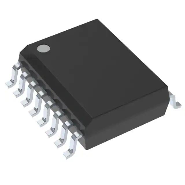
Device Information(1)
PART NUMBER
PACKAGE
BODY SIZE (NOM)
UCC21732-Q1
DW SOIC-16
10.3 mm × 7.5 mm
(1) For all available packages, see the orderable addendum at
the end of the data sheet.
Device Pin Configuration
AIN
1
16
APWM
OC
2
15
VCC
COM
3
14
RST/EN
OUTH
4
13
FLT
VDD
5
12
RDY
OUTL
6
11
,1Å
CLMPE
7
10
IN+
VEE
8
ISOLATION BARRIER
1 Features
9
GND
Not to scale
The UCC21732-Q1 is a galvanic isolated single
channel gate driver designed for SiC MOSFETs and
IGBTs up to 2121-V DC operating voltage with
advanced protection features, best-in-class dynamic
performance and robustness. UCC21732-Q1 has up
to ±10-A peak source and sink current.
1
An IMPORTANT NOTICE at the end of this data sheet addresses availability, warranty, changes, use in safety-critical applications,
intellectual property matters and other important disclaimers. PRODUCTION DATA.
�UCC21732-Q1
SLUSDH7B – FEBURARY 2019 – REVISED SEPTEMBER 2019
www.ti.com
Table of Contents
1
2
3
4
5
6
Features ..................................................................
Applications ...........................................................
Description .............................................................
Revision History.....................................................
Pin Configuration and Functions .........................
Specifications.........................................................
6.1
6.2
6.3
6.4
6.5
6.6
6.7
6.8
6.9
6.10
6.11
6.12
7
1
1
1
2
3
5
Absolute Maximum Ratings ..................................... 5
ESD Ratings ............................................................ 5
Recommended Operating Conditions....................... 5
Thermal Information .................................................. 5
Power Ratings........................................................... 6
Insulation Specifications............................................ 7
Safety-Related Certifications..................................... 8
Safety Limiting Values .............................................. 8
Electrical Characteristics........................................... 9
Switching Characteristics ...................................... 11
Insulation Characteristics Curves ......................... 12
Typical Characteristics .......................................... 13
Parameter Measurement Information ................ 17
7.1 Propagation Delay................................................... 17
7.2 Input Deglitch Filter ................................................. 19
7.3 Active Miller Clamp ................................................. 20
7.4 Under Voltage Lockout (UVLO) .............................. 21
7.5 OC (Over Current) Protection ................................. 23
8
Detailed Description ............................................ 24
8.1
8.2
8.3
8.4
9
Overview .................................................................
Functional Block Diagram .......................................
Feature Description.................................................
Device Functional Modes........................................
24
24
25
31
Applications and Implementation ...................... 32
9.1 Application Information............................................ 32
9.2 Typical Application .................................................. 33
10 Power Supply Recommendations ..................... 47
11 Layout................................................................... 48
11.1 Layout Guidelines ................................................. 48
11.2 Layout Example .................................................... 49
12 Device and Documentation Support ................. 50
12.1
12.2
12.3
12.4
12.5
12.6
Documentation Support .......................................
Receiving Notification of Documentation Updates
Community Resource............................................
Trademarks ...........................................................
Electrostatic Discharge Caution ............................
Glossary ................................................................
50
50
50
50
50
50
13 Mechanical, Packaging, and Orderable
Information ........................................................... 50
4 Revision History
NOTE: Page numbers for previous revisions may differ from page numbers in the current version.
Changes from Revision A (April 2019) to Revision B
•
Changed marketing status from Advance Information to Production Data ........................................................................... 1
Changes from Original (February 2019) to Revision A
2
Page
Submit Documentation Feedback
Page
Copyright © 2019, Texas Instruments Incorporated
Product Folder Links: UCC21732-Q1
�UCC21732-Q1
www.ti.com
SLUSDH7B – FEBURARY 2019 – REVISED SEPTEMBER 2019
5 Pin Configuration and Functions
UCC21732-Q1
DW SOIC (16)
Top View
1
16
APWM
OC
2
15
VCC
COM
3
14
RST/EN
OUTH
4
13
FLT
VDD
5
12
RDY
OUTL
6
11
,1Å
CLMPE
7
10
IN+
VEE
8
ISOLATION BARRIER
AIN
9
GND
Not to scale
Submit Documentation Feedback
Copyright © 2019, Texas Instruments Incorporated
Product Folder Links: UCC21732-Q1
3
�UCC21732-Q1
SLUSDH7B – FEBURARY 2019 – REVISED SEPTEMBER 2019
www.ti.com
Table 1. Pin Functions
PIN
NAME
NO.
I/O (1)
DESCRIPTION
AIN
1
I
Isolated analog sensing input, parallel a small capacitor to COM for better noise immunity
OC
2
I
Over current detection pin, support lower threshold for SenseFET, DESAT, and Shunt resistor sensing
COM
3
P
Common ground reference, connecting to emitter pin for IGBT and source pin for SiC-MOSFET
OUTH
4
O
Gate driver output pull up
VDD
5
P
Positive supply rail for gate drive voltage, Bypassing a >220nF capacitor to COM to support specified gate
driver source peak current capability
OUTL
6
O
Gate driver output pull down
CLMPE
7
O
External Active miller clamp, connecting this pin to the gate of the external miller clamp MOSFET
VEE
8
P
Negative supply rail for gate drive voltage. Bypassing a >220nF capacitor to COM to support specified gate
driver sink peak current capability
GND
9
P
Input power supply and logic ground reference
IN+
10
I
Non-inverting gate driver control input
IN–
11
I
Inverting gate driver control input
RDY
12
O
Power good for VCC-GND and VDD-COM. RDY is open drain configuration and can be paralleled with other
RDY signals
FLT
13
O
Active low fault alarm output upon over current or short circuit. FLT is in open drain configuration and can be
paralleled with other faults
RST/EN
14
I
The RST/EN serves two purposes:
1) Enable / shutdown of the output side. The FET is turned off by a general turn-off, if terminal EN is set to
low;
2) Resets the OC condition signaled on FLT pin. if terminal RST/EN is set to low for more than 1000ns. A
reset of signal FLT is asserted at the rising edge of terminal RST/EN.
For automatic RESET function, this pin only serves as an EN pin. Enable / shutdown of the output side. The
FET is turned off by a general turn-off, if terminal EN is set to low.
VCC
15
P
Input power supply from 3V to 5.5V, bypassing a >100nF capacitor to GND
APWM
16
O
Isolated Analog Sensing PWM output
(1)
4
P = Power, G = Ground, I = Input, O = Output
Submit Documentation Feedback
Copyright © 2019, Texas Instruments Incorporated
Product Folder Links: UCC21732-Q1
�UCC21732-Q1
www.ti.com
SLUSDH7B – FEBURARY 2019 – REVISED SEPTEMBER 2019
6 Specifications
6.1 Absolute Maximum Ratings
over operating free-air temperature range (unless otherwise noted) (1)
PARAMETER
MIN
MAX
UNIT
–0.3
6
V
–0.3
36
V
–17.5
0.3
V
36
V
VCC
VCC – GND
VDD
VDD – COM
VEE
VEE – COM
VMAX
VDD – VEE
–0.3
IN+, IN–, RST/EN
AIN
Reference to COM
OC
Reference to COM
OUTH, OUTL
CLMPE
DC
GND–0.3
VCC
V
Transient, less than 100 ns (2)
GND–5.0
VCC+5.0
V
–0.3
5
V
-0.3
6
DC
VEE–0.3
VDD
V
Transient, less than 100 ns (2)
VEE–5.0
VDD+5.0
V
–0.3
5
V
GND–0.3
Reference to VEE
RDY, FLT, APWM
VCC
V
IFLT, IRDY
FLT, and RDY pin input current
20
mA
IAPWM
APWM pin output current
20
mA
TJ
Junction temperature range
–40
150
°C
Tstg
Storage temperature range
–65
150
°C
(1)
(2)
Stresses beyond those listed under absolute maximum ratings may cause permanent damage to the device. These are stress ratings
only and functional operation of the device at these or any other conditions beyond those indicated under recommended operating
conditions is not implied. Exposure to absolute-maximum-rated conditions for extended periods may affect device reliability.
Values are verified by characterization on bench.
6.2 ESD Ratings
VALUE
V(ESD)
(1)
Electrostatic discharge
Human-body model (HBM), per AEC Q100-002 (1)
±4000
Charged-device model (CDM), per AEC Q100-011
±1500
UNIT
V
AEC Q100-002 indicates that HBM stressing shall be in accordance with the ANSI/ESDA/JEDEC JS-001 specification.
6.3 Recommended Operating Conditions
PARAMETER
MIN
MAX
VCC
VCC–GND
3.0
5.5
UNIT
V
VDD
VDD–COM
13
33
V
VMAX
VDD–VEE
V
–
33
High level input voltage
0.7×VCC
VCC
Low level input voltage
0
0.3×VCC
0.6
4.5
V
IN+, IN–, RST/EN
Reference to GND
V
AIN
Reference to COM
tRST/EN
Minimum pulse width that reset the fault
TA
Ambient Temperature
–40
125
°C
TJ
Junction temperature
–40
150
°C
1000
ns
6.4 Thermal Information
UCC21732-Q1
THERMAL METRIC
(1)
DW (SOIC)
UNIT
16
RθJA
(1)
Junction-to-ambient thermal resistance
68.3
°C/W
For more information about traditional and new thermal metrics, see the Semiconductor and IC Package Thermal Metrics application
report.
Submit Documentation Feedback
Copyright © 2019, Texas Instruments Incorporated
Product Folder Links: UCC21732-Q1
5
�UCC21732-Q1
SLUSDH7B – FEBURARY 2019 – REVISED SEPTEMBER 2019
www.ti.com
Thermal Information (continued)
UCC21732-Q1
THERMAL METRIC (1)
DW (SOIC)
UNIT
16
RθJC(top)
Junction-to-case (top) thermal resistance
27.5
°C/W
RθJB
Junction-to-board thermal resistance
32.9
°C/W
ψJT
Junction-to-top characterization parameter
14.1
°C/W
ψJB
Junction-to-board characterization parameter
32.3
°C/W
6.5 Power Ratings
PARAMETER
PD
Maximum power dissipation (both
sides)
PD1
Maximum power dissipation by
transmitter side
PD2
Maximum power dissipation by
receiver side
6
TEST CONDITIONS
VCC = 5V, VDD-COM = 20V, COM-VEE = 5V, IN+/- = 5V, 150kHz,
50% Duty Cycle for 10nF load, Ta=25oC
Submit Documentation Feedback
Value
UNIT
985
mW
20
mW
965
mW
Copyright © 2019, Texas Instruments Incorporated
Product Folder Links: UCC21732-Q1
�UCC21732-Q1
www.ti.com
SLUSDH7B – FEBURARY 2019 – REVISED SEPTEMBER 2019
6.6 Insulation Specifications
PARAMETER
TEST CONDITIONS
VALUE
UNIT
GENERAL
External clearance (1)
Shortest terminal-to-terminal distance through air
>8
mm
CPG
External creepage (1)
Shortest terminal-to-terminal distance across the
package surface
>8
mm
DTI
Distance through the insulation
Minimum internal gap (Internal clearance) of the
double insulation (2 × 0.0085 mm)
> 17
µm
CTI
Comparative tracking index
DIN EN 60112 (VDE 0303-11); IEC 60112
> 600
V
Material group
According to IEC 60664–1
CLR
Overvoltage Category per IEC 60664–1
I
Rated mains voltage ≤ 300 VRMS
I-IV
Rated mains voltage ≤ 600 VRMS
I-IV
Rated mains voltage ≤ 1000 VRMS
I-III
DIN V VDE V 0884-11 (VDE V 0884-11):2017-01 (2)
VIORM
Maximum repetitive peak isolation voltage AC voltage (bipolar)
VIOWM
Maximum isolation working voltage
VIOTM
Maximum transient isolation voltage
VIOSM
Maximum surge isolation voltage (3)
Apparent charge (4)
qpd
Barrier capacitance, input to output (5)
CIO
Insulation resistance, input to output (5)
RIO
2121
VPK
AC voltage (sine wave) Time dependent dielectric
breakdown (TDDB) test
1500
VRMS
DC voltage
2121
VDC
VTEST=VIOTM, t = 60 s (qualification test)
8000
VTEST=1.2 x VIOTM, t = 1 s (100% production test)
9600
Test method per IEC 62368-1, 1.2/50 µs waveform,
VTEST = 1.6 × VIOSM = 12800 VPK (qualification)
8000
Method a: After I/O safety test subgroup 2/3, Vini =
VIOTM, tini = 60 s; Vpd(m) = 1.2 × VIORM = 2545 VPK,
tm = 10 s
≤5
Method a: After environmental tests subgroup 1,
Vini = VIOTM, tini = 60 s; Vpd(m) = 1.6 × VIORM = 3394
VPK, tm = 10 s
≤5
Method b1: At routine test (100% production) and
preconditioning (type test) Vini = VIOTM, tini = 1 s;
Vpd(m) = 1.875 × VIORM = 3977 VPK, tm = 1 s
≤5
VIO = 0.5 sin (2πft), f = 1 MHz
~1
VIO = 500 V, TA = 25°C
≥ 1012
VIO = 500 V, 100°C ≤ TA ≤ 125°C
≥ 1011
VIO = 500 V at TS = 150°C
≥ 109
Pollution degree
2
Climatic category
40/125/21
VPK
VPK
pC
pF
Ω
UL 1577
VISO
(1)
(2)
(3)
(4)
(5)
Withstand isolation voltage
VTEST = VISO = 5700 VRMS, t = 60 s (qualification);
VTEST = 1.2 × VISO = 6840 VRMS, t = 1 s (100%
production)
5700
VRMS
Apply creepage and clearance requirements according to the specific equipment isolation standards of an application. Care must be
taken to maintain the creepage and clearance distance of a board design to ensure that the mounting pads of the isolator on the printed
circuit board (PCB) do not reduce this distance. Creepage and clearance on a PCB become equal in certain cases. Techniques such as
inserting grooves and ribs on the PCB are used to help increase these specifications.
This coupler is suitable for safe electrical insulation only within the safety ratings. Compliance with the safety ratings shall be ensured by
means of suitable protective circuits.
Testing is carried out in air or oil to determine the intrinsic surge immunity of the isolation barrier.
Apparent charge is electrical discharge caused by a partial discharge (pd).
All pins on each side of the barrier tied together creating a two-terminal device
Submit Documentation Feedback
Copyright © 2019, Texas Instruments Incorporated
Product Folder Links: UCC21732-Q1
7
�UCC21732-Q1
SLUSDH7B – FEBURARY 2019 – REVISED SEPTEMBER 2019
www.ti.com
6.7 Safety-Related Certifications
VDE
UL
Plan to certify according
to DIN V VDE V 0884-11
(VDE V 0884-11):201701;
DIN EN 61010-1 (VDE
0411-1):2011-07
Plan to certify
according to
UL 1577
Component
Recognition
Program
Reinforced insulation
Maximum transient
isolation voltage, 8000
VPK;
Single
Maximum repetitive peak protection,
isolation voltage, 2121
5700 VRMS
VPK;
Maximum surge isolation
voltage, 8000 VPK
Certification Planned
Certification
Planned
CSA
CQC
TUV
Plan to certify according to
GB4943.1-2011
Plan to certify according to
EN 61010-1:2010 (3rd Ed)
and
EN 609501:2006/A11:2009/A1:2010/
A12:2011/A2:2013
Isolation Rating of 5700 VRMS;
Reinforced insulation per CSA
60950-1- 07+A1+A2 and IEC
60950-1 (2nd Ed.), 1450 VRMS
max working voltage (pollution
degree 2, material group I) ;
2 MOPP (Means of Patient
Protection) per CSA 606011:14 and IEC 60601-1 Ed. 3.1,
250 VRMS (354 VPK) max
working voltage
Reinforced Insulation, Altitude
≤ 5000m, Tropical climate,
400 VRMS maximum working
voltage
5700 VRMS Reinforced
insulation per
EN 61010-1:2010 (3rd Ed) up
to working voltage of 1000
VRMS
5700 VRMS Reinforced
insulation per
EN 609501:2006/A11:2009/A1:2010/
A12:2011/A2:2013 up to
working voltage of 1450 VRMS
Certification Planned
Certification Planned
Certification Planned
Plan to certify according to
CSA Component Acceptance
Notice 5A, IEC 60950-1, and
IEC 60601-1
6.8 Safety Limiting Values
The safety-limiting constraint is the maximum junction temperature specified in the data sheet. The power dissipation and
junction-to-air thermal impedance of the device installed in the application hardware determines the junction temperature. The
assumed junction-to-air thermal resistance in the Thermal Information table is that of a device installed on a high-K test board
for leaded surface-mount packages. The power is the recommended maximum input voltage times the current. The junction
temperature is then the ambient temperature plus the power times the junction-to-air thermal resistance. These limits vary
with the ambient temperature, the junction-to-air thermal resistance, and the power supply voltages in different applications.
PARAMETER
IS
Safety input, output, or supply
current
PS
Safety input, output, or total
power
TS
Safety temperature
8
TEST CONDITIONS
MIN
TYP
MAX
UNIT
RθJA =68.3°C/W, VDD = 15V, VEE=-5V, TJ = 150°C, TA
= 25°C
91
RθJA =68.3°C/W, VDD = 20V, VEE=-5V, TJ = 150°C, TA
= 25°C
73
RθJA =68.3°C/W, VDD = 20V, VEE=-5V, TJ = 150°C, TA
= 25°C
1830
mW
150
°C
Submit Documentation Feedback
mA
Copyright © 2019, Texas Instruments Incorporated
Product Folder Links: UCC21732-Q1
�UCC21732-Q1
www.ti.com
SLUSDH7B – FEBURARY 2019 – REVISED SEPTEMBER 2019
6.9 Electrical Characteristics
VCC=3.3V or 5.0V, 1uF capacitor from VCC to GND, VDD–COM=20V, 18V or 15V, COM–VEE =0V, 5V, 8V or 15V,
CL=100pF, –40°C


 工商网监
湘ICP备2023018690号
工商网监
湘ICP备2023018690号
