Sample &
Buy
Product
Folder
Technical
Documents
Support &
Community
Tools &
Software
Reference
Design
UCC28050, UCC28051, UCC38050, UCC38051
SLUS515G – SEPTEMBER 2002 – REVISED DECEMBER 2015
UCC2805x, UCC3805x Transition Mode PFC Controller
1 Features
3 Description
•
The UCC38050 and UCC38051 are PFC controllers
for low-to-medium power applications requiring
compliance with IEC 1000-3-2 harmonic reduction
standard. The controllers are designed for a boost
preregulator operating in transition mode (also
referred to as boundary-conduction mode or critical
conduction-mode operation). They feature a
transconductance voltage amplifier for feedback error
processing, a simple multiplier for generating a
current command proportional to the input voltage, a
current-sense (PWM) comparator, PWM logic, and a
totem-pole driver for driving an external FET.
1
•
•
•
•
•
•
•
•
•
Transition Mode PFC Controller for Low
Implementation Cost
Industry Pin Compatibility With Improved Feature
Set
Improved Transient Response With Slew-Rate
Comparator
Zero Power Detect to Prevent Overvoltage
Protection (OVP) During Light Load Conditions
Accurate Internal VREF for Tight Output
Regulation
Two UVLO Options
OVP, Open-Feedback Protection, and Enable
Circuits
±750-mA Peak Gate Drive Current
Low Start-Up and Operating Currents
Lead (Pb)-Free Packages
In the transition mode operation, the PWM circuit is
self-oscillating, with the turnon being governed by an
inductor zero-current detector (ZCD pin), and the
turnoff being governed by the current-sense
comparator. Additionally, the controller provides
features such as peak current limit, default timer,
overvoltage protection (OVP) and enable.
Device Information(1)
2 Applications
•
•
•
•
Single-Stage PFC Flyback Converters for Lighting
and Motor Drives
Switch-Mode Power Supplies for Desktops,
Monitors, TVs, and Set Top Boxes (STBs)
AC Adapter Front-End Power Supplies
Electronic Ballasts
PART NUMBER
UCC28050,
UCC28051,
UCC38050,
UCC38051
PACKAGE
BODY SIZE (NOM)
SOIC (8)
3.91 mm × 4.90 mm
PDIP (8)
6.35 mm × 9.81 mm
(1) For all available packages, see the orderable addendum at
the end of the data sheet.
Simplified Application Diagram
UCC38050
1
VO_SNS VCC
2
COMP
3
MULTIN
4
CS
8
DRV
7
GND
6
ZCD
5
UDG−02125
1
An IMPORTANT NOTICE at the end of this data sheet addresses availability, warranty, changes, use in safety-critical applications,
intellectual property matters and other important disclaimers. PRODUCTION DATA.
�UCC28050, UCC28051, UCC38050, UCC38051
SLUS515G – SEPTEMBER 2002 – REVISED DECEMBER 2015
www.ti.com
Table of Contents
1
2
3
4
5
6
7
Features ..................................................................
Applications ...........................................................
Description .............................................................
Revision History.....................................................
Pin Configuration and Functions .........................
Specifications.........................................................
1
1
1
2
3
4
6.1
6.2
6.3
6.4
6.5
6.6
4
4
4
4
5
7
Absolute Maximum Ratings ......................................
ESD Ratings..............................................................
Recommended Operating Conditions.......................
Thermal Information ..................................................
Electrical Characteristics...........................................
Typical Characteristics ..............................................
Detailed Description ............................................ 10
7.1 Overview ................................................................. 10
7.2 Functional Block Diagram ....................................... 11
7.3 Feature Description................................................. 12
7.4 Device Functional Modes........................................ 14
8
Application and Implementation ........................ 16
8.1 Application Information............................................ 16
8.2 Typical Application ................................................. 16
9 Power Supply Recommendations...................... 21
10 Layout................................................................... 22
10.1 Layout Guidelines ................................................. 22
10.2 Layout Example .................................................... 22
11 Device and Documentation Support ................. 23
11.1
11.2
11.3
11.4
11.5
11.6
Device Support......................................................
Related Links ........................................................
Community Resources..........................................
Trademarks ...........................................................
Electrostatic Discharge Caution ............................
Glossary ................................................................
23
23
23
23
23
23
12 Mechanical, Packaging, and Orderable
Information ........................................................... 24
4 Revision History
Changes from Revision F (March 2009) to Revision G
•
2
Page
Added ESD Ratings table, Feature Description section, Device Functional Modes, Application and Implementation
section, Power Supply Recommendations section, Layout section, Device and Documentation Support section, and
Mechanical, Packaging, and Orderable Information section. ................................................................................................ 1
Submit Documentation Feedback
Copyright © 2002–2015, Texas Instruments Incorporated
Product Folder Links: UCC28050 UCC28051 UCC38050 UCC38051
�UCC28050, UCC28051, UCC38050, UCC38051
www.ti.com
SLUS515G – SEPTEMBER 2002 – REVISED DECEMBER 2015
5 Pin Configuration and Functions
D or P Package
8-Pin SOIC or PDIP
Top View
VO_SNS 1
8
VCC
COMP 2
7
DRV
MULTIN 3
6
GND
CS 4
5
ZCD
Pin Functions
PIN
NAME
COMP
CS
NO.
2
4
I/O
DESCRIPTION
O
Output of the transconductance error amplifier. Loop compensation components are connected
between this pin and ground. The output current capability of this pin is 10-μA under normal
conditions, but increases to approximately 1-mA when the differential input is greater than the
specified values in the specifications table. This voltage is one of the inputs to the multiplier, with
a dynamic input range of 2.5 V to 3.8 V. During zero power or overvoltage conditions, this pin
goes below 2.5 V nominal. When it goes below 2.3 V, the zero power comparator is activated,
which prevents the gate drive from switching.
I
This pin senses the instantaneous switch current in the boost switch and uses it as the internal
ramp for PWM comparator. The internal circuitry filters out switching noise spikes without
requiring external components. In addition, an external R-C filter may be required to suppress the
noise spikes. An internal clamp on the multiplier output terminates the switching cycle if this pin
voltage exceeds 1.7 V. Additional external filtering may be required. CS threshold is
approximately equal to:
2
L=
(V AC(min))
(
× V OUT –
√2 × VAC(min))
2 × F s(min) × V OUT × P IN
(1)
VOFFSET is approximately 75 mV to improve the zero crossing distortion.
DRV
7
O
The gate drive output for an external boost switch. This output is capable of delivering up to 750mA peak currents during turn-on and turn-off. An external gate drive resistor may be needed to
limit the peak current depending on the VCC voltage being used. Below the UVLO threshold, the
output is held low.
GND
6
–
The chip reference ground. All bypassing elements are connected to ground pin with shortest
loops feasible.
MULTIN
3
I
This pin senses the instantaneous boost regulator input voltage through a voltage divider. The
voltage acts as one of the inputs to the internal multiplier. Recommended operating range is 0 V
to 2.5 V at high line.
–
The supply voltage for the chip. This pin should be bypassed with a high-frequency capacitor
(greater than 0.1-μF) and tied to GND. The UCC38050 has a wide UVLO hysteresis of
approximately 6.3 V that allows use of a lower value supply capacitor on this pin for quicker and
easier start-up. The UCC38051 has a narrow UVLO hysteresis with of about 2.8 V, and a startup voltage of about 12.5 V for applications where the operation of the PFC device must be
controlled by a downstream PWM controller.
I
This pin senses the boost regulator output voltage through a voltage divider. Internally, this pin is
the inverting input to the transconductance amplifier (with a nominal value of 2.5 V) and also is
input to the OVP comparator. Additionally, pulling this pin below the ENABLE threshold turns off
the output switching, ensuring that the gate drive is held off while the boost output is precharging, and also ensuring no runaway if the feedback path is open.
I
Input for the zero current detect comparator. The boost inductor current is indirectly sensed
through the bias winding on the boost inductor. The ZCD pin input goes low when the inductor
current reaches zero and that transition is detected. Internal active voltage clamps are provided
to prevent this pin from going below ground or too high. If zero current is not detected within 400
μs, a reset timer sets the latch and gate drive.
VCC
VO_SNS
ZCD
8
1
5
Copyright © 2002–2015, Texas Instruments Incorporated
Submit Documentation Feedback
Product Folder Links: UCC28050 UCC28051 UCC38050 UCC38051
3
�UCC28050, UCC28051, UCC38050, UCC38051
SLUS515G – SEPTEMBER 2002 – REVISED DECEMBER 2015
www.ti.com
6 Specifications
6.1 Absolute Maximum Ratings
over operating free-air temperature range (unless otherwise noted) (1)
MIN
MAX
UNIT
20
V
IDD
30
mA
ZCD
±10
mA
Gate drive current (peak), IDRV
DRV
±750
mA
Input voltage, VCC
VO_SNS, MULTIN, CS
5
V
Maximum negative voltage
VO_SNS, MULTIN, DRV, CS
–0.5
V
D package
650
mW
Supply voltage, VCC
(Internally clamped)
Input current into VCC clamp
Input current
Power dissipation at TA = 50°C
1
W
Operating junction temperature range, TJ
P package
–55
150
°C
Storage temperature, Tstg
–65
150
°C
300
°C
Lead temperature 1,6 mm (1/16 inch)
from case for 10 seconds
(1)
Stresses beyond those listed under Absolute Maximum Ratings may cause permanent damage to the device. These are stress ratings
only, which do not imply functional operation of the device at these or any other conditions beyond those indicated under Recommended
Operating Conditions. Exposure to absolute-maximum-rated conditions for extended periods may affect device reliability.
6.2 ESD Ratings
VALUE
UNIT
Human-body model (HBM), per ANSI/ESDA/JEDEC JS-001 (1)
±2000
V
Charged-device model (CDM), per JEDEC specification JESD22C101 (2)
±500
V
SOIC PACKAGE
V(ESD)
(1)
(2)
Electrostatic discharge
JEDEC document JEP155 states that 500-V HBM allows safe manufacturing with a standard ESD control process.
JEDEC document JEP157 states that 250-V CDM allows safe manufacturing with a standard ESD control process.
6.3 Recommended Operating Conditions
over operating free-air temperature range (unless otherwise noted)
MIN
VCC input voltage from a low-impedance source
Operating junction temperature, TJ
NOM
MAX
UNIT
VCCOFF + 1 V
18
V
–40
125
°C
6.4 Thermal Information
UCC2805x, UCC3805x
THERMAL METRIC (1)
D (SOIC)
P (PDIP)
UNIT
8 PINS
8 PINS
RθJA
Junction-to-ambient thermal resistance
113.6
55.6
°C/W
RθJC(top)
Junction-to-case (top) thermal resistance
60.3
45.5
°C/W
RθJB
Junction-to-board thermal resistance
54.3
32.7
°C/W
ψJT
Junction-to-top characterization parameter
14
23.1
°C/W
ψJB
Junction-to-board characterization parameter
53.8
32.6
°C/W
(1)
4
For more information about traditional and new thermal metrics, see the Semiconductor and IC Package Thermal Metrics application
report, SPRA953.
Submit Documentation Feedback
Copyright © 2002–2015, Texas Instruments Incorporated
Product Folder Links: UCC28050 UCC28051 UCC38050 UCC38051
�UCC28050, UCC28051, UCC38050, UCC38051
www.ti.com
SLUS515G – SEPTEMBER 2002 – REVISED DECEMBER 2015
6.5 Electrical Characteristics
TA = 0°C to 70°C for the UCC3805x, –40°C to +105°C for the UCC2805x, TA = TJ, VCC = 12 V.
PARAMETER
TEST CONDITIONS
MIN
TYP
MAX
UNIT
18
19
20
V
75
125
µA
SUPPLY
VCC operating voltage
18
V
Shunt voltage
IVCC = 25 mA
Supply current, off
VCC = VCC turnon threshold –300 mV
Supply current, disabled
VO_SNS = 0.5 V
2
4
mA
Supply current, on
75 kHz, CL = 0 nF
4
6
mA
Supply current, dynamic operating
75 kHz, CL = 1 nF
5
7
mA
UVLO
VCC turnon threshold
UCCx8050
15.4
15.8
16.4
UCCx8051
12
12.5
13
VCC turnoff threshold
UVLO hysteresis
9.4
9.7
10
UCCx8050
5.8
6.3
6.8
UCCx8051
2.3
2.8
3.3
UCC3805x
2.46
2.5
2.54
UCC2805x
2.45
2.5
2.55
V
V
V
VOLTAGE AMPLIFIER (VO_SNS)
Input voltage (VREF)
Input bias current
VCOMP high
VO_SNS = 2.1 V
VCOMP low
VO_SNS = 2.55 V
gM
TJ = 25 °C, VCOMP = 3.5 V
Source current
4.5
60
V
0.5
µA
5.5
V
1.8
2.45
V
90
130
µS
UCCx8050
VO_SNS = 2.1 V, VCOMP = 3.5 V
–0.2
–0.1
UCCx8051
VO_SNS = 2.1 V, VCOMP = 2.5 V
–200
–300
VO_SNS = 2.7 V, VCOMP = 3.5 V
0.2
1
UCCx8050
VREF + 0.165
VREF + 0.19
VREF + 0.21
UCCx8051
VREF + 0.15
VREF + 0.18
VREF + 0.21
UCCx8050
175
200
225
UCCx8051
150
180
210
UCCx8050
0.62
0.67
0.72
UCCx8051
0.18
0.23
0.28
0.05
0.1
0.2
V
0.87
1/V
Sink current
mA
–400
µA
mA
OVER VOLTAGE PROTECTION / ENABLE
Overvoltage reference
Hysteresis
Enable threshold
Enable hysteresis
V
mV
V
MULTIPLIER
Multiplier gain constant (k)
VMULTIN = 0.5 V, COMP = 3.5 V
Dynamic input range, VMULTIN INPUT
Dynamic input range, COMP INPUT
0.43
0.65
0 to 2.5
0 to 3.5
2.5 to 3.8
2.5 to 4
Input bias current, MULTIN
V
V
0.1
1
µA
2.3
2.5
V
ZERO POWER
Zero power comparator threshold (1)
(1)
Measured on VCOMP
2.1
Ensured by design. Not production tested.
Copyright © 2002–2015, Texas Instruments Incorporated
Submit Documentation Feedback
Product Folder Links: UCC28050 UCC28051 UCC38050 UCC38051
5
�UCC28050, UCC28051, UCC38050, UCC38051
SLUS515G – SEPTEMBER 2002 – REVISED DECEMBER 2015
www.ti.com
Electrical Characteristics (continued)
TA = 0°C to 70°C for the UCC3805x, –40°C to +105°C for the UCC2805x, TA = TJ, VCC = 12 V.
PARAMETER
TEST CONDITIONS
MIN
TYP
MAX
UNIT
ZERO CURRENT DETECT
Input threshold (rising edge) (1)
1.5
1.7
2
Hysteresis (1)
250
350
450
5
6
0.3
0.65
0.9
200
400
Input high clamp
I = 3 mA
Input low clamp
I = −3 mA
Restart time delay
V
mV
V
V
µs
CURRENT SENSE COMPARATOR
Input bias current
Input offset voltage
CS = 0 V
(1)
0.1
1
µA
10
mV
300
450
ns
1.7
1.8
V
Ω
–10
Delay to output
CS to DRV
Maximum current sense threshold voltage
1.55
PFC GATE DRIVER
6
GT1 pull-up resistance
IOUT = –125 mA
5
12
GT1 pull-down resistance
IOUT = 125 mA
2
10
Ω
GT1 output rise time
CLOAD = 1 nF, RLOAD = 10 Ω
25
75
ns
GT1 output fall time
CLOAD = 1 nF, RLOAD = 10 Ω
10
50
ns
Submit Documentation Feedback
Copyright © 2002–2015, Texas Instruments Incorporated
Product Folder Links: UCC28050 UCC28051 UCC38050 UCC38051
�UCC28050, UCC28051, UCC38050, UCC38051
www.ti.com
SLUS515G – SEPTEMBER 2002 – REVISED DECEMBER 2015
6.6 Typical Characteristics
4.0
6
ICC = ON
75 kHZ, 1 nF
5
ICC − Supply Current − mA
3.0
2.5
2.0
UCC38050
1.5
UCC38051
ICC − Supply Current − mA
3.5
1.0
0.5
4
8
12
VCC − Supply Voltage − V
16
2
0
−50
20
Figure 1. Supply Current vs Supply Voltage
ICC = ON
No Switching
−25
0
75
25
50
− Temperature − °C
100
125
Figure 2. Supply Current vs Temperature
20
2.60
UVLO ON
(UCCx8050)
18
2.58
16
VREF − Reference Voltage − V
VUVLO − UVLO Threshold VOltage − V
ICC = ON
75 kHZ, No Load
3
1
0
0
4
UVLO ON
(UCCx8051)
14
12
UVLO OFF
10
8
6
UVLO HYSTERESIS (UCCx8050)
4
2.56
2.54
2.52
2.50
2.48
2.46
2.44
2
2.42
UVLO HYSTERESIS (UCCx8051)
0
−50
−25
0
25
50
75
TJ − Temperature − °C
100
2.40
−50
125
100
125
1.800
COMP = 3.5 V
1.4
1.2
COMP = 3.25 V
1.0
0.8
0.6
COMP = 3 V
COMP = 2.5 V
0.4
0.2
COMP = 2.75 V
0
0.5
1.0
1.5
2.0
2.5
VMULTIN − Multiplier Input Voltage− V
3.0
Figure 5. Current Sense Input Threshold vs Multiplier Input
Voltage
Copyright © 2002–2015, Texas Instruments Incorporated
VCS(max)− Maximum Current Sense Threshold − V
COMP = 3.75 V
1.6
VCS − CS Input Voltage − V
0
25
50
75
TJ − Temperature − °C
Figure 4. Reference Voltage vs Temperature
Figure 3. UVLO Thresholds vs Temperature
1.8
0.0
−25
1.775
1.750
1.725
1.700
1.675
1.650
1.625
1.600
1.575
1.550
−50
−25
0
25
50
75
TJ − Temperature − °C
100
125
Figure 6. Maximum Current Sense Threshold vs
Temperature
Submit Documentation Feedback
Product Folder Links: UCC28050 UCC28051 UCC38050 UCC38051
7
�UCC28050, UCC28051, UCC38050, UCC38051
SLUS515G – SEPTEMBER 2002 – REVISED DECEMBER 2015
www.ti.com
Typical Characteristics (continued)
120
400
gM − Transconductance − µS
tDELAY − Cureent Sense to Output Delay Time − ns
450
350
300
250
200
150
100
90
80
100
70
50
0
−50
−25
0
25
50
75
TJ − Temperature − °C
100
60
−50
125
Figure 7. CS To Output Delay Time vs Temperature
0
25
50
75
TJ − Temperature − °C
100
125
ICOMP − gM Amplifier Output Current − mA
0.012
1.0
0.5
UCCx8051
0
−0.5
UCCx8050
−1.0
−1.5
2.0
−25
Figure 8. Transconductance vs Temperature
1.5
ICOMP − gM Amplifier Output Current − mA
110
2.1
2.2
2.3
2.4
2.5
2.6
2.7
2.8
0.008
0.004
0
−0.004
−0.008
−0.012
2.40
VVO_SNS − Output Sense Voltage − V
Figure 9. gM Amplifier Output Current vs Output Sense
Voltage
2.45
2.50
2.55
2.60
VVO_SNS − Output Sense Voltage − V
Figure 10. gM Amplifier Output Current vs Output Sense
Voltage (Small Signal View)
5.5
2.80
5.0
2.75
VSENSE
4.5
4.0
3.5
3.0
VAO
2.5
2.0
2.70
2.65
OVP ON
2.60
2.55
OVP OFF
2.50
2.45
1.5
25 µs / div
Figure 11. Voltage Amplifier Output vs Time (UCC38050)
8
VOVP − OVP Threshold Voltage − V
VCOMP − Voltage Amplifier Output − V
CLOAD = 10 nF
Submit Documentation Feedback
2.40
−50
−25
0
25
50
75
TJ − Temperature − °C
100
125
Figure 12. Overvoltage Protection Thresholds vs
Temperature
Copyright © 2002–2015, Texas Instruments Incorporated
Product Folder Links: UCC28050 UCC28051 UCC38050 UCC38051
�UCC28050, UCC28051, UCC38050, UCC38051
www.ti.com
SLUS515G – SEPTEMBER 2002 – REVISED DECEMBER 2015
Typical Characteristics (continued)
10
600
8
500
tRESTART − Restart Time − µs
IZCD − ZCD Current − mA
6
4
2
0
−2
−4
−6
400
300
200
100
−8
−10
0
0
1
2
3
4
5
6
7
−50
−25
0
VZCD − ZCD Voltage − V
100
125
Figure 14. Restart Time vs Temperature
Figure 13. Zero Current Detection Clamp Current vs Voltage
8
2.5
VCC = 12 V
VCC = 12 V
VOUT(sat) − Output Saturation Voltage − V
VOUT(sat) − Output Saturation Voltage − V
25
50
75
TJ − Temperature − °C
7
6
5
4
3
2
1
0
2.0
1.5
1.0
0.5
0
0
100
200
300
400
500
600
700
800
ISOURCE − Source Current − mA
Figure 15. Output Saturation Voltage vs Source Current
Copyright © 2002–2015, Texas Instruments Incorporated
0
100
200 300 400 500 600
ISINK − Sink Current − mA
700
800
Figure 16. Output Saturation Voltage vs Sink Current
Submit Documentation Feedback
Product Folder Links: UCC28050 UCC28051 UCC38050 UCC38051
9
�UCC28050, UCC28051, UCC38050, UCC38051
SLUS515G – SEPTEMBER 2002 – REVISED DECEMBER 2015
www.ti.com
7 Detailed Description
7.1 Overview
The UCC38050 and UCC38051 are PFC controllers for low-to-medium power applications requiring compliance
with IEC 1000-3-2 harmonic reduction. The controller is designed for a boost preregulator operating in transition
mode (also referred to as boundary-conduction mode or critical conduction-mode operation). It features a
transconductance voltage amplifier for feedback error processing, a simple multiplier for generating a current
command proportional to the input voltage, a current-sense (PWM) comparator, PWM logic, and a totem-pole
driver for driving an external FET.
The UCC38050 and UCC38051, while being pin-compatible with other industry controllers providing similar
functionality, offer many feature enhancements and tighter specifications, leading to an overall reduction in
system implementation cost. The system performance is enhanced by incorporation of a zero-power detect
function, which allows the controller output to shut down at light load conditions without running into overvoltage.
The device also features innovative slew rate enhancement circuits, which improve the large signal transient
performance of the voltage error amplifier. The low start-up and operating currents of the device result in low
power consumption and ease of start-up. Highly accurate internal bandgap reference leads to tight regulation of
output voltage in normal and OVP conditions, resulting in higher system reliability. The enable comparator
ensures that the controller is off if the feedback sense path is broken or if the input voltage is very low.
There are two key parameteric differences between UCC38050 and UCC38051. The UVLO turn-on threshold of
UCC38050 is 15.8 V, while for UCC38051 it is 12.5 V. Secondly, the gM amplifier source current for UCC38050
is typically 1.3 mA, while for UCC38051 it is 300 μA. The higher UVLO turn-on threshold of the UCC38050
allows quicker and easier start-up with a smaller VCC capacitance, while the lower UVLO turn-on threshold of
UCC38051 allows the operation of the PFC chip to be easily controlled by the downsteam PWM controller in twostage power converters. The UCC38050 gM amplifier also provides a full 1.3-mA typical source current for faster
start-up and improved transient response when output is low, either at start-up or during transient conditions. The
UCC38051 scales this source current back down to 300-μA typical source current to gradually increase the error
voltage, preventing a step increase in line currents at start-up, but still providing good transient response. The
UCC38051 is suitable for multiple applications, including AC adapters, where a two-stage power conversion is
needed. The UCC38050 is suitable for applications such as electronic ballasts, where there is no down-stream
PWM conversion and the advantages of a smaller VCC capacitor and improved transient response can be
realized.
10
Submit Documentation Feedback
Copyright © 2002–2015, Texas Instruments Incorporated
Product Folder Links: UCC28050 UCC28051 UCC38050 UCC38051
�UCC28050, UCC28051, UCC38050, UCC38051
www.ti.com
SLUS515G – SEPTEMBER 2002 – REVISED DECEMBER 2015
7.2 Functional Block Diagram
2.7/2.5 V
+
0.67/0.57 V
0.23/0.15 V
V0_SNS
2.5 V
COMP
MULTIN
ENABLE
VREF
GOOD
REF
8
VCC
7
DRV
6
GND
5
ZCD
OVP
x
x MULT
+
PWM
+
2
ZERO
POWER
DETECT
3
R
Q
S
Q
TIMER
+
2.3 V
+
40 k:
CS
UVLO
+
VREF AND
BIAS REG
INT. BIAS
gm VOL.
ERROR AMP
1
VREF
OVP
+
4
1.7/1.4 V
5 pF
Copyright © 2002–2015, Texas Instruments Incorporated
Submit Documentation Feedback
Product Folder Links: UCC28050 UCC28051 UCC38050 UCC38051
11
�UCC28050, UCC28051, UCC38050, UCC38051
SLUS515G – SEPTEMBER 2002 – REVISED DECEMBER 2015
www.ti.com
7.3 Feature Description
7.3.1 UVLO and Reference Block
This block generates a precision reference voltage used to obtain tightly controlled UVLO threshold. In addition
to generating a 2.5-V reference for the non-inverting terminal of the gM amplifier, it generates the reference
voltages for blocks such as OVP, enable, zero power, and multiplier. An internal rail of 7.5 V is also generated, to
drive all the internal blocks.
7.3.2 Error Amplifier
The voltage error amplifier in UCC3805x is a transcoductance amplifier, with a typical transconductance value of
90 μS. A transconductance amplifier is advantageous in that the inverting input of the amplifier is solely
determined by the external resistive-divider from the output voltage, and not the transient behavior of the
amplifier itself. This allows the VO_SNS pin to be used for sensing overvoltage conditions.
The sink and source capability of the error amplifier is approximately 10 μA during normal operation of the
amplifier. However, when the VO_SNS pin voltage is beyond the normal operating conditions (VO_SNS > 1.05 ×
VREF, VO_SNS < 0.88 × VREF), additional circuitry to enhance the slew-rate of the amplifier is activated.
Enhanced slew-rate of the compensation capacitor results in a faster start-up and transient response. This
prevents the output voltage from drifting too high or too low, which can happen if the compensation capacitor
were to be slewed by the normal slewing current of 10 μA. When VO_SNS rises above the normal range, the
enhanced sink current capability is in excess of 1 mA. When VO_SNS falls below the normal range, the
UCC38050 can source more than 1 mA, and the UCC38051 sources approximately 300 μA. The limited source
current in the UCC38051 helps to gradually increase the error voltage on the COMP pin preventing a step
increase in line current. The actual rate of increase of VCOMP depends on the compensation network connected
to the COMP pin.
7.3.3 Zero Current Detection and Re-Start Timer Blocks
When the boost inductor current becomes zero, the voltage at the power MOSFET drain end falls. This is
indirectly sensed with a secondary winding connected to the ZCD pin. The internal active clamp circuitry prevents
the voltage from going to a negative or a high positive value. The clamp has the sink and source capability of 10
mA. The resistor value in series with the secondary winding should be chosen to limit the ZCD current to less
than 10 mA. The rising edge threshold of the ZCD comparator can be as high as 2 V. The auxiliary winding
should be chosen such that the positive voltage (when the power MOSFET is off) at the ZCD pin is in excess of
2 V.
The restart timer attempts to set the gate drive high in case the gate drive remains off for more than 400 μs
nominally. The minimum guaranteed time period of the timer is 200 μs. This translates to a minimum switching
frequency of 5 kHz. In other words, the boost inductor value should be chosen for switching frequencies greater
than 5 kHz.
12
Submit Documentation Feedback
Copyright © 2002–2015, Texas Instruments Incorporated
Product Folder Links: UCC28050 UCC28051 UCC38050 UCC38051
�UCC28050, UCC28051, UCC38050, UCC38051
www.ti.com
SLUS515G – SEPTEMBER 2002 – REVISED DECEMBER 2015
Feature Description (continued)
7.3.4 Enable Block
The gate drive signal is held low if the voltage at the VO_SNS pin is less than the ENABLE threshold. This
feature can disable the converter by pulling VO_SNS low. If the output feedback path is broken, VO_SNS is
pulled to ground, and the output is disabled to protect the power stage.
7.3.5 Zero Power Block
When the output of the gM amplifier goes below 2.3 V, the zero power comparator latches the gate drive signal
low. The slew rate enhancement circuitry of the gM amplifier activated during overvoltage conditions slews the
COMP pin to approximately 2.4 V. This ensures that the zero power comparator is not activated during transient
behavior, when the slew rate enhancement circuitry is enhanced.
7.3.6 Multiplier Block
The multiplier block has two inputs. One is the error amplifier output voltage (VCOMP), and the other is VMULTIN,
which is obtained by a resistive divider from the rectified line. The multiplier output is approximately 0.67 ×
VMULTIN × (VCOMP − 2.5 V). There is a positive offset of about 75 mV to the VMULTIN signal because this improves
the zero-crossing distortion and thus the THD performance of the controller in the application. The dynamic
range of the inputs can be found in Electrical Characteristics.
7.3.7 Overvoltage Protection (OVP) Block
The OVP feature in the part is not activated under most operating conditions because of the presence of the slew
rate enhancement circuitry present in the error amplifier. As soon as the output voltage reaches to approximately
5% to 7% above the nominal value, the slew rate enhancement circuit is activated, and the error amplifier output
voltage is pulled below the dynamic range of the multiplier block. This prevents further rise in output voltage.
If the COMP pin is not pulled low fast enough and the voltage rises further, the OVP circuit acts as a second line
of protection. When the voltage at the VO_SNS pin is more than 7.5% of the nominal value (> (VREF + 0.19)), the
OVP feature is activated. It stops the gate drive from switching as long as the voltage at the VO_SNS pin is
above the nominal value (VREF). This prevents the output DC voltage from going above 7.5% of the nominal
value designed for, and protects the switch and other components of the system such as the boost capacitor.
Copyright © 2002–2015, Texas Instruments Incorporated
Submit Documentation Feedback
Product Folder Links: UCC28050 UCC28051 UCC38050 UCC38051
13
�UCC28050, UCC28051, UCC38050, UCC38051
SLUS515G – SEPTEMBER 2002 – REVISED DECEMBER 2015
www.ti.com
7.4 Device Functional Modes
7.4.1 Transition Mode Control
The boost converter, the most common topology used for power factor correction, can operate in two modes:
continuous conduction code (CCM) and discontinuous conduction mode (DCM). Transition mode control, also
referred to as critical conduction mode (CRM) or boundary conduction mode, maintains the converter at the
boundary between CCM and DCM by adjusting the switching frequency.
The CRM converter typically uses a variation of hysteretic control, with the lower boundary equal to zero current.
It is a variable frequency control technique that has inherently stable input current control while eliminating
reverse recovery rectifier losses. As shown in Figure 17, the switch current is compared to the reference signal
(output of the multiplier) directly. This control method has the advantage of simple implementation and good
power factor correction.
L
VAC
D
Q
C
Load
RIAC
IAC
ZCD
X
÷ MULT
X
IMO
+
S
R
Q
Gate Driver
Logic
VEA
+
VREF
UDG−02124
Figure 17. Basic Block Diagram of CRM Boost PFC
The power stage equations and the transfer functions of the CRM are the same as the CCM. However,
implementations of the control functions are different. Transition mode forces the inductor current to operate just
at the border of CCM and DCM. The current profile is also different, and affects the component power loss and
filtering requirements. The peak current in the CRM boost is twice the amplitude of CCM, leading to higher
conduction losses. The peak-to-peak ripple is twice the average current, which affects MOSFET switching losses
and magnetics ac losses.
14
Submit Documentation Feedback
Copyright © 2002–2015, Texas Instruments Incorporated
Product Folder Links: UCC28050 UCC28051 UCC38050 UCC38051
�UCC28050, UCC28051, UCC38050, UCC38051
www.ti.com
SLUS515G – SEPTEMBER 2002 – REVISED DECEMBER 2015
Device Functional Modes (continued)
IAVERAGE
(a) CCM
IPEAK
IAVERAGE
(b) DCM
IPEAK
IAVERAGE
Note: Operating Frequency >> 120 Hz
(C) CRM
UDG−02123
Figure 18. PFC Inductor Current Profiles
For low to medium power applications up to approximately 300 W, the CRM boost has an advantage in losses.
The filtering requirement is not severe, and therefore is not a disadvantage. For medium to higher power
applications, where the input filter requirements dominate the size of the magnetics, the CCM boost is a good
choice due to lower peak currents (which reduces conduction losses) and lower ripple current (which reduces
filter requirements). The main tradeoff in using CRM boost is lower losses due to no reverse recovery in the
boost diode vs. higher ripple and peak currents.
Copyright © 2002–2015, Texas Instruments Incorporated
Submit Documentation Feedback
Product Folder Links: UCC28050 UCC28051 UCC38050 UCC38051
15
�UCC28050, UCC28051, UCC38050, UCC38051
SLUS515G – SEPTEMBER 2002 – REVISED DECEMBER 2015
www.ti.com
8 Application and Implementation
NOTE
Information in the following applications sections is not part of the TI component
specification, and TI does not warrant its accuracy or completeness. TI’s customers are
responsible for determining suitability of components for their purposes. Customers should
validate and test their design implementation to confirm system functionality.
8.1 Application Information
The UCC38050 and UCC38051 are switch-mode controllers used in boost converters for power factor correction
operating in transition mode. In the transition mode operation, the PWM circuit is self-oscillating, with the turnon
being governed by an inductor zero-current detector (ZCD pin), and the turnoff being governed by the currentsense comparator. Additionally, the controller provides features such as peak current limit, default timer, OVP,
and enable.
There are two key parametric differences between UCC38050 and UCC38051. The UVLO turnon threshold of
UCC38050 is 15.8 V, while for UCC38051 it is 12.5 V. Secondly, the gM amplifier source current for UCC38050
is typically 1.3 mA, while for UCC38051 it is 300 μA. The UCC38051 is suitable for multiple applications,
including AC adapters, where a two-stage power conversion is needed. The UCC38050 is suitable for
applications such as electronic ballasts, where there is no down-stream PWM conversion and the advantages of
a smaller VCC capacitor and improved transient response can be realized. Figure 19 is an example of a critical
conduction mode power factor correction boost converter utilizing the UCC38050.
8.2 Typical Application
The UCC38050 is used for the off-line power factor corrected pre-regulator with operation over a universal input
range of 85 V to 265 V with a 400-VDC regulated output. The schematic is shown in Figure 19, and the board
layout for the reference design is shown in Figure 24.
+
+
+
Figure 19. Universal Line Input 100-W Boost Converter
16
Submit Documentation Feedback
Copyright © 2002–2015, Texas Instruments Incorporated
Product Folder Links: UCC28050 UCC28051 UCC38050 UCC38051
�UCC28050, UCC28051, UCC38050, UCC38051
www.ti.com
SLUS515G – SEPTEMBER 2002 – REVISED DECEMBER 2015
Typical Application (continued)
RUP
−
RAC1
+
RG1
L
COUT
RB
RZC
RS1
RO1
2.7/2.5 V
V REF
OVP
+
INT. BIAS
CB
UVLO
VREF AND
BIAS REG
+
VCC
VO_SNS
ENABLE
+
0.67/0.57 V (50)
0.23/0.15 V (51)
REF
V REF
GOOD
gM E/A
8
OVP
1
2.5 V
RO2
x
÷ MULT
x
+
COMP
7
PWM
+
R
Q
S
Q
DRV
2
MULTIN
CV1
ZERO
POWER
DETECT
3
CV2
RV1
RAC2
RV1
2.3 V
CS
GND
6
TIMER
+
+
40 k Ω
1.7 V/1.4 V
ZCD
4
CAC1
5
5 pF
CS1
UDG−02008
Figure 20. Typical Application Diagram
8.2.1 Design Requirements
Table 1 shows the design requirements for a CCM, PFC boost converter utilizing the UCC38050.
Table 1. UCC38050 Design Requirements
PARAMETER
VIN
TEST CONDITION
Input voltage
MIN
TYP
85
Input frequency
MAX
UNIT
265
VRMS
60
Hz
VOUT
Output voltage DC
VIN = 85 VRMS
370
400
425
V
VOUT
Output voltage DC
VIN = 265 VRMS
370
390
410
V
POUT
Output power
100
W
0
Output voltage ripple
VIN = 85 VRMS
Efficiency
POUT = 100 W
Total harmonic distortion
(THD)
VIN = 85 VRMS, POUT = 100 W
5%
Total harmonic distortion
(THD)
VIN = 265 VRMS, POUT = 100 W
15%
Hold-up time
3%
90%
16.7
Copyright © 2002–2015, Texas Instruments Incorporated
Submit Documentation Feedback
Product Folder Links: UCC28050 UCC28051 UCC38050 UCC38051
ms
17
�UCC28050, UCC28051, UCC38050, UCC38051
SLUS515G – SEPTEMBER 2002 – REVISED DECEMBER 2015
www.ti.com
8.2.2 Detailed Design Procedure
For a selected VOUT and minimum switching frequency, the following equations outline the design guidelines for
power stage component selection, using a universal input, 100-W PFC converter with an output voltage of 390 V.
Refer to Figure 20 for reference designators.
8.2.2.1 Inductor Selection
In the transition mode control, the inductor value must be calculated to start the next switching cycle at zero
current. The time it takes to reach zero depends on line voltage and inductance and as shown in Equation 2. L
determines the frequency range of the converter.
2
L=
(V AC(min))
(
)
√
× V OUT – 2 × V AC(min)
2 × F s(min) × V OUT × P IN
where
•
•
•
VAC = RMS line voltage
VAC(min) = minimum AC line voltage
PIN = maximum input power averaged over the ac line period
IL(peak) = 2 × √2 × (PIN/VAC(min))
IL(rms) = IL(peak) / √6
(2)
(3)
(4)
8.2.2.2 MOSFET Selection
The main switch selection is driven by the amount of power dissipation allowable. Choose a device that
minimizes gate charge and capacitance, and minimizes the sum of switching and conduction losses at a given
frequency.
I Q(rms_crm) =
√
1 – (4 × 2 ) ×
√
6
V
) × ILPEAK(crm)
( 9 πAC(min)
× V OUT
(5)
(6)
VQ(max) = VOUT
8.2.2.3 Diode Selection
The effects of the reverse recovery current in the diode can be eliminated with relatively little negative impact to
the system. The diode selection is based on reverse voltage, forward current, and switching speed.
ID(avg) = IOUT(avg)
(7)
I D(rms) = I L(peak)
√
√2 × VAC
π × V OUT
(8)
(9)
VD(peak) = VOUT
8.2.2.4 Capacitor Selection
The hold-up time is the main requirement in determining the output capacitance. ESR and the maximum RMS
ripple current rating can also be important, especially at higher power levels.
COUT(min) = (2 × POUT × tHOLDUP) / ((VOUT)2 – (VOUT(min))2)
where
•
VOUT(min) = minimum regulator input voltage for operation
I C(rms) =
18
√(
2
)
I L(peak)
×
√2 × VAC(max)
Submit Documentation Feedback
π × V OUT
–
(
P OUT
V OUT
(10)
2
)
+ (ac rms load currents)
2
(11)
Copyright © 2002–2015, Texas Instruments Incorporated
Product Folder Links: UCC28050 UCC28051 UCC38050 UCC38051
�UCC28050, UCC28051, UCC38050, UCC38051
www.ti.com
SLUS515G – SEPTEMBER 2002 – REVISED DECEMBER 2015
8.2.2.5 Multiplier Set-Up
Select RAC1 and RAC2 so that their ratio uses the full dynamic range of the multiplier input at the peak line
voltage, and yet with values small enough to negate the effects of the multiplier bias current. To use the
maximum range of the multiplier, select the divider ratio so that VMULTIN, evaluated at the peak of the maximum
ac line voltage, is the maximum of the minimum dynamic input range of MULTIN, which is 2.5 V. Choose RAC1 so
that it has at least 100 μA at the peak of the minimum AC operating line voltage.
R AC1
√2 V
– 1
=
2.5 AC(max)
R AC2
(12)
)
(
In extreme cases, switching transients can contaminate the MULTIN signal, so it can be beneficial to add
capacitor CAC1. Select the value of CAC1 so that the corner frequency of the resulting filter is greater than the
lowest switching frequency. The low corner frequency of this filter may compromise the overall power factor.
8.2.2.6 Sense Resistor Selection
The current sense resistor value must be chosen to limit the output power, and it must also use the full dynamic
range of the multiplier during normal steady state operation. The value of RS1 is thus selected for maximum
power operation at low ac line voltage conditions. To use the full dynamic range, set the VSENSE threshold as a
function of the dynamic input range of VCOMP and the peak of the minimum MULTIN voltage.
R S1 =
0.67 × (COMP(MAX) – COMP (MIN)) × (MULTIN (PEAK)@VAC(min) – 0.075)
2 × √2 ×
P IN(max)
V AC(min)
where
•
•
•
COMP(MAX) = 3.8 V
COMP(MIN) = 2.5 V
MULTIN(PEAK)@VAC(min) = √2 × VAC(min)( RAC2 / (RAC2+RAC1) )
(13)
If the exact value RS1 is not available, RS2 and RS3 can be added for further scaling. The CS pin already has an
internal filter for noise due to switching transients. Additional filtering at switching transient frequencies can be
achieved by adding CS1.
8.2.2.7 Output Voltage Sense Design
Select the divider ratio of RO1 and RO2 to set the VO_SNS voltage to 2.5 V at the desired output voltage. The
current through the divider should be at least 200 μA.
8.2.2.8 Voltage Loop Design
How well the voltage control loop is designed directly impacts line current distortion. UCC38050 employs a
transconductance amplifier (gM amp) with gain scheduling for improved transient response (refer to Figure 9).
Integral type control at low frequencies is preferred, because the loop gain varies considerably with line
conditions. The largest gain occurs at maximum line voltage. If the power factor corrector load is dc-to-dc
switching converter, the small signal model of the controller and the power factor corrector, from COMP to PFC
output voltage is given by:
2
^
V OUT(s)
^
V COMP(s)
=
V OUT(avg)
k 1 × (V AC)
× 1
× R S1 × k CRM × C OUT S
where
•
•
•
•
^VOUT = small signal variations in VOUT
^VCOMP = small signal variations in VCOMP
k1 = multiplier gain = 0.65
kCRM = peak to average factor = 2
Copyright © 2002–2015, Texas Instruments Incorporated
(14)
Submit Documentation Feedback
Product Folder Links: UCC28050 UCC28051 UCC38050 UCC38051
19
�UCC28050, UCC28051, UCC38050, UCC38051
SLUS515G – SEPTEMBER 2002 – REVISED DECEMBER 2015
www.ti.com
A controller that has integral control at low frequencies requires a zero near the crossover frequency to be stable.
The resulting gM amplifier configuration is shown in Figure 21.
VOUT
+
CV1
CV2
V REF
RV1
Figure 21. gM Amplifier Configuration
The compensator transfer function is:
1 R V1 u C V1 u s
gM
AV
u
C V1 C V2
§ §
ªC u C V2 ¼º · ·
s ¨ 1 ¨ R V1 u ¬ V1
¸ u s¸
¨ ¨
C V1 u C V2 º¼ ¸¹ ¸
ª
¬
©
©
¹
where
•
gM = DC transconductance gain = 100 μs
(15)
The limiting factor of the gain is usually the allowable third harmonic distortion, although other harmonics can
dominate. The crossover frequency of the control loop will be much lower than twice the AC line voltage. To
choose the compensator dynamics, determine the maximum allowable loop gain at twice the line frequency, and
solve for capacitor CV2. This also determines the crossover frequency.
§
·
§ VAC(max) ·
gM u k1
¸
C V2 ¨
¸2u¨
¨ VOUT(avg) u RS1 u k(crm) u COUT(max loop gainat 2f ) ¸
© 4SfAC ¹
AC ¹
©
(16)
fCO
VAC
S
gM u k1
C V2 u VOUT u RS1 u k(cmr) u COUT
(17)
Select CV1 so that the low frequency zero is one-tenth of the crossover frequency.
CV1 = 9 CV2
(18)
Select RV1 so that the pole is at the crossover frequency.
≈ 1 / 2π fCO CV2
20
(19)
Submit Documentation Feedback
Copyright © 2002–2015, Texas Instruments Incorporated
Product Folder Links: UCC28050 UCC28051 UCC38050 UCC38051
�UCC28050, UCC28051, UCC38050, UCC38051
www.ti.com
SLUS515G – SEPTEMBER 2002 – REVISED DECEMBER 2015
8.2.3 Application Curves
Figure 22 and Figure 23 show the input current and rectified line for the power module.
• Channel 3 = Rectified Line Voltage
• Channel 4 = Power Module Input Current
VIN = 85 V
POUT = 100 W
Figure 22. Rectified Line Voltage and Power Module Input
Current at 85 V/100 W
VIN = 265 V
POUT = 100 W
Figure 23. Rectified Line Voltage and Power Module Input
Current at 265 V/100 W
9 Power Supply Recommendations
The supply voltage for the device comes from VCC pin. This pin must be bypassed with a high-frequency
capacitor (greater than 0.1 μF) and tied to GND. The UCC38050 has a wide UVLO hysteresis of approximately
6.3 V that allows use of a lower value supply capacitor on this pin for quicker and easier start-up. The UCC38051
has a narrow UVLO hysteresis with of about 2.8 V, and a start-up voltage of about 12.5 V for applications where
the operation of the PFC device must be controlled by a downstream PWM controller.
Copyright © 2002–2015, Texas Instruments Incorporated
Submit Documentation Feedback
Product Folder Links: UCC28050 UCC28051 UCC38050 UCC38051
21
�UCC28050, UCC28051, UCC38050, UCC38051
SLUS515G – SEPTEMBER 2002 – REVISED DECEMBER 2015
www.ti.com
10 Layout
10.1 Layout Guidelines
10.1.1 Bias Current
The bias voltage is supplied by a bias winding on the inductor. Select the turns ratio so that sufficient bias
voltage can be achieved at low AC line voltage. The bias capacitor must be large enough to maintain sufficient
voltage with AC line variations. Connect a 0.1-μF bypass capacitor between the VCC pin and the GND pin as
close to the integrated circuit as possible. For wide line variations, a resistor, RB, is necessary to permit clamping
action. The bias voltage should also be clamped with an external zener diode to a maximum of 18 V.
10.1.2 Zero Current Detection
The zero current detection activates when the ZCD voltage falls below 1.4 V. The bias winding can provide the
necessary voltage. This pin has a clamp at approximately 5 V. Add a current limiting resistor, RZC, to keep the
maximum current below 1 mA.
10.2 Layout Example
Figure 24. UCC38050 Layout Example
Figure 25. UCC38050 Bottom-Layer Layout Example
22
Submit Documentation Feedback
Copyright © 2002–2015, Texas Instruments Incorporated
Product Folder Links: UCC28050 UCC28051 UCC38050 UCC38051
�UCC28050, UCC28051, UCC38050, UCC38051
www.ti.com
SLUS515G – SEPTEMBER 2002 – REVISED DECEMBER 2015
11 Device and Documentation Support
11.1 Device Support
11.1.1 Development Support
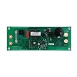
Reference Design, 100-W Universal Line Input PFC Boost Converter Using the UCC38050 (SLUU134)
11.2 Related Links
The table below lists quick access links. Categories include technical documents, support and community
resources, tools and software, and quick access to sample or buy.
Table 2. Related Links
PARTS
PRODUCT FOLDER
SAMPLE & BUY
TECHNICAL
DOCUMENTS
TOOLS &
SOFTWARE
SUPPORT &
COMMUNITY
UCC28050
Click here
Click here
Click here
Click here
Click here
UCC28051
Click here
Click here
Click here
Click here
Click here
UCC38050
Click here
Click here
Click here
Click here
Click here
UCC38051
Click here
Click here
Click here
Click here
Click here
11.3 Community Resources
The following links connect to TI community resources. Linked contents are provided "AS IS" by the respective
contributors. They do not constitute TI specifications and do not necessarily reflect TI's views; see TI's Terms of
Use.
TI E2E™ Online Community TI's Engineer-to-Engineer (E2E) Community. Created to foster collaboration
among engineers. At e2e.ti.com, you can ask questions, share knowledge, explore ideas and help
solve problems with fellow engineers.
Design Support TI's Design Support Quickly find helpful E2E forums along with design support tools and
contact information for technical support.
11.4 Trademarks
E2E is a trademark of Texas Instruments.
All other trademarks are the property of their respective owners.
11.5 Electrostatic Discharge Caution
These devices have limited built-in ESD protection. The leads should be shorted together or the device placed in conductive foam
during storage or handling to prevent electrostatic damage to the MOS gates.
11.6 Glossary
SLYZ022 — TI Glossary.
This glossary lists and explains terms, acronyms, and definitions.
Copyright © 2002–2015, Texas Instruments Incorporated
Submit Documentation Feedback
Product Folder Links: UCC28050 UCC28051 UCC38050 UCC38051
23
�UCC28050, UCC28051, UCC38050, UCC38051
SLUS515G – SEPTEMBER 2002 – REVISED DECEMBER 2015
www.ti.com
12 Mechanical, Packaging, and Orderable Information
The following pages include mechanical, packaging, and orderable information. This information is the most
current data available for the designated devices. This data is subject to change without notice and revision of
this document. For browser-based versions of this data sheet, refer to the left-hand navigation.
24
Submit Documentation Feedback
Copyright © 2002–2015, Texas Instruments Incorporated
Product Folder Links: UCC28050 UCC28051 UCC38050 UCC38051
�PACKAGE OPTION ADDENDUM
www.ti.com
20-May-2022
PACKAGING INFORMATION
Orderable Device
Status
(1)
Package Type Package Pins Package
Drawing
Qty
Eco Plan
(2)
Lead finish/
Ball material
MSL Peak Temp
Op Temp (°C)
Device Marking
(3)
Samples
(4/5)
(6)
UCC28050D
ACTIVE
SOIC
D
8
75
RoHS & Green
NIPDAU
Level-1-260C-UNLIM
-40 to 105
28050
Samples
UCC28050DR
ACTIVE
SOIC
D
8
2500
RoHS & Green
NIPDAU
Level-1-260C-UNLIM
-40 to 105
28050
Samples
UCC28050P
ACTIVE
PDIP
P
8
50
RoHS & Green
NIPDAU
N / A for Pkg Type
-40 to 105
28050
Samples
UCC28051D
ACTIVE
SOIC
D
8
75
RoHS & Green
NIPDAU
Level-1-260C-UNLIM
-40 to 105
28051
Samples
UCC28051DG4
ACTIVE
SOIC
D
8
75
RoHS & Green
NIPDAU
Level-1-260C-UNLIM
-40 to 105
28051
Samples
UCC28051DR
ACTIVE
SOIC
D
8
2500
RoHS & Green
NIPDAU
Level-1-260C-UNLIM
-40 to 105
28051
Samples
UCC28051DRG4
ACTIVE
SOIC
D
8
2500
RoHS & Green
NIPDAU
Level-1-260C-UNLIM
-40 to 105
28051
Samples
UCC28051P
ACTIVE
PDIP
P
8
50
RoHS & Green
NIPDAU
N / A for Pkg Type
-40 to 105
28051
Samples
UCC38050D
ACTIVE
SOIC
D
8
75
RoHS & Green
NIPDAU
Level-1-260C-UNLIM
0 to 70
38050
Samples
UCC38050DR
ACTIVE
SOIC
D
8
2500
RoHS & Green
NIPDAU
Level-1-260C-UNLIM
0 to 70
38050
Samples
UCC38050P
ACTIVE
PDIP
P
8
50
RoHS & Green
NIPDAU
N / A for Pkg Type
0 to 70
38050
Samples
UCC38051D
ACTIVE
SOIC
D
8
75
RoHS & Green
NIPDAU
Level-1-260C-UNLIM
0 to 70
38051
Samples
(1)
The marketing status values are defined as follows:
ACTIVE: Product device recommended for new designs.
LIFEBUY: TI has announced that the device will be discontinued, and a lifetime-buy period is in effect.
NRND: Not recommended for new designs. Device is in production to support existing customers, but TI does not recommend using this part in a new design.
PREVIEW: Device has been announced but is not in production. Samples may or may not be available.
OBSOLETE: TI has discontinued the production of the device.
(2)
RoHS: TI defines "RoHS" to mean semiconductor products that are compliant with the current EU RoHS requirements for all 10 RoHS substances, including the requirement that RoHS substance
do not exceed 0.1% by weight in homogeneous materials. Where designed to be soldered at high temperatures, "RoHS" products are suitable for use in specified lead-free processes. TI may
reference these types of products as "Pb-Free".
RoHS Exempt: TI defines "RoHS Exempt" to mean products that contain lead but are compliant with EU RoHS pursuant to a specific EU RoHS exemption.
Green: TI defines "Green" to mean the content of Chlorine (Cl) and Bromine (Br) based flame retardants meet JS709B low halogen requirements of


 工商网监
湘ICP备2023018690号
工商网监
湘ICP备2023018690号
