��������� ��������� �������
�� ��������� ��������� �������
�
�
��
�
�
�� �� ���� � ����� �
� � ����
�
SLUS215B − OCTOBER 1998 − REVISED FEBRUARY 2004
D Precision Positive Linear Series Pass
D
D
D
D
D
D
D
D
D
Voltage Regulation
0.45 V Dropout at 3 A
50 mV Dropout at 10 mA
Quiescent Current Under 650 µA
Irrespective of Load
Adjustable (5-Lead) Output Voltage Version
Fixed (3-Lead) Versions for 3.3-V and 5-V
Outputs
Logic Shutdown Capability
Short-Circuit Power Limit of
(3% × VIN × ISHORT)
Low VOUT to VIN Reverse Leakage
Thermal Shutdown
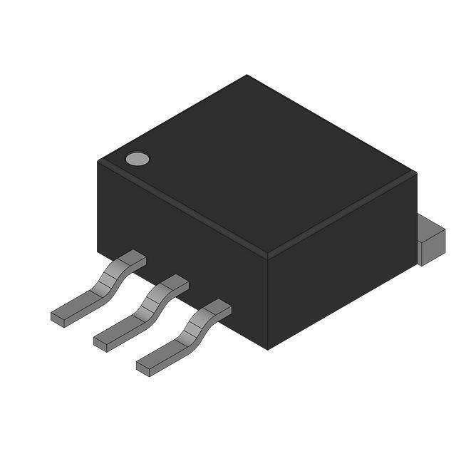
TO−263−3 TD PACKAGE
(FRONT VIEW)
TO−263−5 TD PACKAGE
(FRONT VIEW)
5
4
3
2
1
VOUT
ADJ
GND
CT
VIN
3
2
1
VOUT
GND
VIN
TO−220−5 T PACKAGE
(FRONT VIEW)
+
5
4
3
2
1
VOUT
ADJ
GND
CT
VIN
TO−220−3 T PACKAGE
(FRONT VIEW)
description
The UCC283−3/−5/−ADJ family of positive linear
series pass voltage regulators are tailored for
low-drop-out applications where low quiescent
power is important. Fabricated with a BiCMOS
technology ideally suited for low input-to-output
differential applications, the UCC283−5 passes
3 A while requiring only 0.45 V of typical input
voltage headroom (ensured 0.6-V dropout).
+
3
2
VOUT
1
VIN
GND
These regulators include reverse voltage sensing that prevents current in the reverse direction. Quiescent
current is always less than 650 µA. These devices have been internally compensated in such a way that the
need for a minimum output capacitor has been eliminated.
UCC283−3 and UCC283−5 versions are in 3-lead packages and have preset outputs at 3.3 V and 5.0 V
respectively. The output voltage is regulated to 1.5% at room temperature. The UCC283−ADJ version, in a
5-lead package, regulates the output voltage programmed by an external resistor ratio.
Short-circuit current is internally limited. The device responds to a sustained overcurrent condition by turning
off after a tON time delay. The device then stays off for a period, tOFF, that is 32 times the tON delay. The device
then begins pulsing on and off at the tON/(tON+tOFF) duty cycle of 3%. This drastically reduces the power
dissipation during short-circuit and means heat sinks need only accommodate normal operation. On the
3-leaded versions of the device tON is fixed at 750 µs, on the adjustable 5-leaded versions an external capacitor
sets the on time. The off time is always 32 × tON. The external timing control pin, CT, on the 5-leaded versions
also serves as a shutdown input when pulled low.
Internal power dissipation is further controlled with thermal overload protection circuitry. Thermal shutdown
occurs if the junction temperature exceeds 165°C. The chip remains off until the temperature has dropped 20°C.
The UCC283 series is specified for operation over the industrial range of −40°C to 85°C, and the UCC383 series
is specified from 0°C to 70°C. These devices are available in 3- and 5-pin TO−220 and TO−263 power packages.
Please be aware that an important notice concerning availability, standard warranty, and use in critical applications of
Texas Instruments semiconductor products and disclaimers thereto appears at the end of this data sheet.
All trademarks are the property of their respective owners.
Copyright 1998−2004, Texas Instruments Incorporated
��
����
�
� �����!"#��� �$ %&��'�# "$ �� (&)*�%"#��� +"#',
���+&%#$ %�����! #� $('%���%"#���$ ('� #-' #'�!$ �� �'."$ ��$#�&!'�#$
$#"�+"�+ /"��"�#0, ���+&%#��� (��%'$$��1 +�'$ ��# �'%'$$"��*0 ��%*&+'
#'$#��1 �� "** ("�"!'#'�$,
POST OFFICE BOX 655303
• DALLAS, TEXAS 75265
1
���������� ��������� �������
�� ��������� ��������� �������
�
�
��
�
�
�� �� ���� � ����� �
� � ����
�
SLUS215B − OCTOBER 1998 − REVISED FEBRUARY 2004
AVAILABLE OPTIONS(1)
TA
OUTPUT VOLTAGE (V)
MIN
−40°C
−40
C to 85
85°C
C
TYP
MAX
TO−220−5
TD
T
3.22
3.3
3.58
UCC283TD−3
—
UCC283T−3
4.875
5.00
5.125
UCC283TD−5
—
UCC283T−5
—
—
UCC283TD−ADJ
—
UCC283T−ADJ
—
UCC383T−3
—
ADJ
0°C
70°C
0
C to 70
C
PACKAGE DEVICES
TO−263−5(2)
TO−220−3
TO−263−3(2)
—
3.22
3.3
3.58
UCC383TD−3
4.875
5.00
5.125
UCC383TD−5
—
UCC383T−5
—
—
UCC383TD−ADJ
—
UCC383T−ADJ
ADJ
1. For more package and ordering information, see the Package Option Addendum located at the end of this data sheet.
2. For 50 piece reel, add KTTT (e.g., UCC283TDKTTT−3); for 500 piece reel, add TR (e.g., UCC283TDTR−3).
functional block diagram
VIN
*5 LEADED VERSION ONLY (ADJ)
VOUT
VPUMP
CURRENT LIMIT
ADJ*
4 A/ 7 A CURRENT
REFERENCE
R2
+
+
0.65 V
SD/CT*
R1
1.25 V
3% DUTY CYCLE
CURRENT LIMIT TIMER
GND
REVERSE VOLTAGE
SENSE
UVLO
THERMAL
SHUTDOWN
R2
R1
0
OPEN
UCC283−3
82k
50k
UCC283−5
150k
50k
UCC283−ADJ
UDG−98133
2
POST OFFICE BOX 655303
• DALLAS, TEXAS 75265
���������� ��������� �������
�� ��������� ��������� �������
�
�
��
�
�
�� �� ���� � ����� �
� � ����
�
SLUS215B − OCTOBER 1998 − REVISED FEBRUARY 2004
electrical characteristics TA = 0°C to 70°C for the UCC383−x series, TA = −40°C to 85°C for the
UCC283−x, VVIN = VVOUT + 1.5 V, IOUT = 10 mA, CIN = 10 mF, COUT = 22 mF. For the UCC283−ADJ, VVIN
= 6.5 V, VOUT = 5.0 V, CT = 750 pF, TJ = TA unless otherwise stated
PARAMETER
TEST CONDITIONS
MIN
TYP
MAX
UNITS
UCC283−5 Fixed 5 V, 3 A Family
Output voltage
Line regulation
TJ = 25°C
Over temperature
4.925
4.875
Load regulation
VVIN = 5.15 V to 9 V
IOUT = 10 mA to 3 A
Dropout voltage, VDROPOUT = VVIN − VVOUT
IOUT = 3 A,
IOUT = 1.5 A,
VOUT = 4.85 V
VOUT = 4.85 V
IOUT = 10 mA,
VVOUT = 0 V
VOUT = 4.85 V
Peak current limit
Overcurrent threshold
Current limit duty cycle
Overcurrent time out, tON
VVOUT = 0 V
VVOUT = 0 V
Quiescent current
No load
Reverse leakage current
Undervoltage lockout
5
1 V < VVIN < VVOUT,
VVOUT ≤ 5.1 V, at VVOUT
VIN where VOUT passes current
5.075
5.125
2
V
V
10
mV
10
20
mV
0.4
0.6
V
0.2
0.45
V
50
150
mV
4
7
10
A
3
4
5.5
A
3%
5%
400
750
1400
µs
400
650
µA
30
75
µA
2.5
2.8
3
V
3.25
3.3
3.35
V
UCC283−3 Fixed 3.3 V, 3 A Family
Output voltage
Line regulation voltage
TJ = 25°C
Over temperature
3.22
3.38
V
Load regulation voltage
VVIN = 3.45 V to 9 V
IOUT = 10 mA to 3 A
7
15
mV
VOUT = 3.15 V
0.5
1
V
Dropout voltage, VDROPOUT = VVIN − VVOUT
IOUT = 3A,
IOUT = 1.5A,
VOUT = 3.15 V
0.25
0.6
V
IOUT = 10mA,
VVOUT = 0 V
VOUT = 3.15 V
50
150
mV
Peak current limit
7
10
A
A
4
Overcurrent threshold
Current limit duty cycle
3
Overcurrent time out, tON
VVOUT = 0 V
VVOUT = 0 V
Quiescent current
No load
Reverse leakage current
Undervoltage lockout
400
1 V < VVIN < VVOUT,
VVOUT ≤ 3.35 V at VVOUT
VIN where VOUT passes current
POST OFFICE BOX 655303
• DALLAS, TEXAS 75265
2.5
2
7
mV
4
5.5
3%
5%
750
1400
µs
400
650
µA
30
75
µA
2.8
3
V
3
���������� ��������� �������
�� ��������� ��������� �������
�
�
��
�
�
�� �� ���� � ����� �
� � ����
�
SLUS215B − OCTOBER 1998 − REVISED FEBRUARY 2004
electrical characteristics TA = 0°C to 70°C for the UCC383−x series, TA = −40°C to 85°C for the
UCC283−x, VVIN = VVOUT + 1.5 V, IOUT = 10 mA, CIN = 10 mF, COUT = 22 mF. For the UCC283−ADJ, VVIN
= 6.5 V, VOUT = 5.0 V, CT = 750 pF, TJ = TA unless otherwise stated
PARAMETER
TEST CONDITIONS
MIN
TYP
MAX
UNITS
UCC283−ADJ Adjustable Output, 3 A Family
Regulating voltage at ADJ pin
Line regulation voltage, at ADJ input
TJ = 25°C
1.23
Over temperature
1.22
Load regulation voltage, at ADJ input
VVIN = VVOUT + 150 mV to 9 V
IOUT = 10 mA to 3 A
Dropout voltage, VDROPOUT = VIN − VOUT
VOUT = 4.85 V,
VOUT = 4.85 V,
IOUT = 3 A
IOUT = 1.5 A
VOUT = 4.85 V,
VVOUT = 0 V
IOUT = 10 mA
Peak current limit
Overcurrent threshold
Current limit duty cycle
Overcurrent time out, tON
Reverse leakage current
VVOUT = 0 V
VVOUT = 0 V
No load
At CT input
Quiescent current in shutdown
VVIN = 9 V
VIN where VOUT passes current
UVLO
V
V
3
mV
mV
2
5
0.4
0.6
V
0.2
0.45
V
50
150
mV
4
7
10
A
3
4
5.5
A
3
5
%
300
575
1200
µs
30
100
µA
20
250
nA
400
650
µA
Bias current at ADJ input
Shutdown threshold
1.27
1.28
1
1 V < VVIN < VVOUT
VVOUT ≤ 9 V, at VVOUT
Quiescent current
1.25
0.25
0.65
V
40
75
µA
2.5
2.8
3
V
absolute maximum ratings over operating free-air temperature (unless otherwise noted)†
Input voltage
VIN . . . . . . . . . . . . . . . . . . . . . . . . . . . . . . . . . . . . . . . . . . . . . . . . . . . . . . . . . . . . . . . . . . . . . . . . . . . . . . . . . . . . . 9 V
CT . . . . . . . . . . . . . . . . . . . . . . . . . . . . . . . . . . . . . . . . . . . . . . . . . . . . . . . . . . . . . . . . . . . . . . . . . . . . −0.3 V to 3 V
ADJ . . . . . . . . . . . . . . . . . . . . . . . . . . . . . . . . . . . . . . . . . . . . . . . . . . . . . . . . . . . . . . . . . . . . . . . . . . . −0.3 V to 9 V
Storage Temperature, Tstg . . . . . . . . . . . . . . . . . . . . . . . . . . . . . . . . . . . . . . . . . . . . . . . . . . . . . . . . −65°C to 150°C
Junction Temperature, TJ . . . . . . . . . . . . . . . . . . . . . . . . . . . . . . . . . . . . . . . . . . . . . . . . . . . . . . . . . −55°C to 150°C
Lead Temperature (soldering, 10 seconds) . . . . . . . . . . . . . . . . . . . . . . . . . . . . . . . . . . . . . . . . . . . . . . . . . . 300°C
† Stresses beyond those listed under “absolute maximum ratings” may cause permanent damage to the device. These are stress ratings only, and
functional operation of the device at these or any other conditions beyond those indicated under “recommended operating conditions” is not
implied. Exposure to absolute-maximum-rated conditions for extended periods may affect device reliability.
4
POST OFFICE BOX 655303
• DALLAS, TEXAS 75265
���������� ��������� �������
�� ��������� ��������� �������
�
�
��
�
�
�� �� ���� � ����� �
� � ����
�
SLUS215B − OCTOBER 1998 − REVISED FEBRUARY 2004
pin descriptions
ADJ: Adjust pin for the UCC283−ADJ version only. Feedback pin for the linear regulator. Program the output
voltage with R1 connected from ADJ to GND and R2 connected from VOUT to ADJ. Output voltage is given
by:
V
OUT
+
1.25 V
(R1 ) R2)
R1
CT: Short-circuit timing capacitor and shutdown input for the UCC283−ADJ version. Pulling CT below 0.25 V
turns off the regulator and places it in a low quiescent-current mode. A timing capacitor, C, from CT to GND
programs the duration of the pulsed short-circuit on-time. On-time, tON, is approximately given by:
t
ON
+ 750 k
C
GND: Reference ground.
VIN: Input voltage, This pin must be bypassed with a low ESL/ESR 1-µF or larger capacitor to GND. VIN can
range from (VOUT + VDROPOUT) to 9 V. If VIN is reduced to zero while VOUT is held high, the reverse leakage
from VOUT to VIN is less than 75µA.
VOUT: Regulated output voltage. A bypass capacitor is not required at VOUT, but may be desired for good
transient response. The bypass capacitor must not exceed a maximum value in order to insure the regulator
can start.
APPLICATION INFORMATION
overview
The UCC383 family of low dropout linear (LDO) regulators provide a regulated output voltage for applications
with up to 3 A of load current. The regulators feature a low dropout voltage and short-circuit protection, making
their use ideal for demanding high-current applications requiring fault protection.
short-circuit-protection
The UCC383 provides unique short-circuit protection circuitry that reduces power dissipation during a fault.
When an overload situation is detected, the device enters a pulsed mode of operation at 3% duty cycle reducing
the heat sink requirements during a fault. The UCC383 has two current thresholds that determine its behavior
during a fault as shown in Figure 1. When the regulator current exceeds the overcurrent threshold for a period
longer than tON, the UCC383 shuts off for a period (tOFF) which is 32 × tON. During an overload, the regulator
actively limits the maximum current to the peak current limit value. The peak current limit is nominally 3 A
greater than the overcurrent threshold. The regulator continues in pulsed mode until the fault is cleared as
illustrated in Figure 1.
POST OFFICE BOX 655303
• DALLAS, TEXAS 75265
5
���������� ��������� �������
�� ��������� ��������� �������
�
�
��
�
�
�� �� ���� � ����� �
� � ����
�
SLUS215B − OCTOBER 1998 − REVISED FEBRUARY 2004
APPLICATION INFORMATION
PEAK
CURRENT
LIMIT
OUTPUT
CURRENT
OVERLOAD
OVER−
CURRENT
THRESHOLD
IO (NOM)
VO (NOM)
ROLICL
OUTPUT
VOLTAGE
TON
32 TON
TON
32 TON
TON
32 TON
Figure 1. UCC383 Short-Circuit Timing
A capacitive load on the regulator’s output appears as a short-circuit during start-up. If the capacitance is too
large, the output voltage does not come into regulation during the initial tON period and the UCC383 enters
pulsed mode operation. The peak current limit, tON period, and load characteristics determine the maximum
value of output capacitor that can be charged. For a constant current load the maximum output capacitance is
given as follows:
C
OUT(max)
ǒ CL * ILOADǓ
+ I
t
V
ON
Farads
OUT
(1)
For worst case calculations, the minimum values of on time (tON) and peak current limit (ICL) should be used.
The adjustable version allows the tON time to be adjusted with a capacitor on the CT pin:
t
ON(adj)
+ 750, 000
C (m Farad) microseconds
(2)
For a resistive load (RLOAD) the maximum output capacitor can be estimated from:
t
C
OUT(max)
+
ȡ
R
6
ON(sec)
LOAD
ȏnȧ
ȣ
ȧ
Ȥ
Farads
1
VOUT
1*
I
R
CL
LOAD
Ȣ
POST OFFICE BOX 655303
(3)
• DALLAS, TEXAS 75265
���������� ��������� �������
�� ��������� ��������� �������
�
�
��
�
�
�� �� ���� � ����� �
� � ����
�
SLUS215B − OCTOBER 1998 − REVISED FEBRUARY 2004
APPLICATION INFORMATION
dropout performance
Referring to the Block Diagram, the dropout voltage of the UCC383 is equal to the minimum voltage drop (VIN
to VOUT) across the N-channel MOSFET. The dropout voltage is dependent on operating conditions such as
load current, input and load voltages, as well as temperature. The UCC383 achieves a low Rds(on) through the
use of an internal charge-pump (VPUMP) that drives the MOSFET gate. Figure 2 depicts typical dropout voltages
versus load current for the 3.3-V and 5-V versions of the part, as well as the adjustable version programmed
to 3.0 V.
Figure 3 depicts the typical dropout performance of the adjustable version with various output voltages and load
currents.
Operating temperatures also affect the Rds(on) and dropout voltage of the UCC383. Figure 4 graphs the typical
dropout for the 3.3-V and 5-V versions with a 3-A load over temperature.
TYPICAL DROPOUT VOLTAGE
vs.
LOAD CURRENT
0.5
TYPICAL DROPOUT VOLTAGE
vs.
IOUT AND VOUT
0.8
VOUT = 3.3 V
0.7
0.6
VIN−VOUT (V)
VIN−VOUT (V)
0.4
VOUT = 3 V
0.3
VOUT = 5 V
0.2
0.5
I OUT= 3 A
0.4
I OUT= 1.5 A
0.3
0.2
0.1
0.1
0
I OUT= 1 A
0
1
1.5
2
2.5
3
IOUT (A)
3
3.5
4
VOUT (V)
4.5
5
Figure 3
Figure 2
POST OFFICE BOX 655303
• DALLAS, TEXAS 75265
7
���������� ��������� �������
�� ��������� ��������� �������
�
�
��
�
�
�� �� ���� � ����� �
� � ����
�
SLUS215B − OCTOBER 1998 − REVISED FEBRUARY 2004
APPLICATION INFORMATION
voltage programming and shutdown feature for adjustable version
A typical application circuit based on the UCC383 adjustable version is shown in Figure 5. The output voltage
is externally programmed through a resistive divider at the ADJ pin.
TYPICAL DROPOUT VOLTAGE
vs.
CASE TEMPERATURE WITH A 3-A LOAD
VIN − VOUT (V)
0.6
0.5
V OUT = 3.3 V
0.4
V OUT = 5 V
0.3
0.2
−40
10
60
Temperature (5C)
Figure 4
V
OUT
+ 1.25
ǒ1 ) R2
Ǔ Volts
R1
(4)
The maximum programmed output voltage is constrained by the 9-V absolute rating of the IC (this includes the
charge pump voltage) and its ability to enhance the N-channel MOSFET. Unless the load current is below the
3-A rating of the device, output voltages above 7 V are not recommended. The minimum output voltage can
be programmed down to 1.25 V. However, the input voltage must always be greater than the UVLO of the part.
The adjustable version includes a shutdown feature, limiting quiescent current to 40 µA typical. The UCC383
is shut down by pulling the CT pin to below 0.25 V. As shown in Figure 5, a small logic level MOSFET or BJT
transistor in parallel with the timing capacitor can be driven with a digital signal, putting the device in shutdown.
If the CT pin is not pulled low, the IC internally pulls up the pin enabling the regulator. The CT pin should not
be forced high, as this interferes with the short-circuit-protection feature. Selection of the timing capacitor is
explained in Short-Circuit-Protection.
The adjustable version can be used in applications requiring remote voltage sensing (i.e. monitoring a voltage
other than or not directly tied to the VOUT pin). This is possible since the inverting input of the error-voltage
amplifier (see Block Diagram) is brought out to the ADJ pin.
8
POST OFFICE BOX 655303
• DALLAS, TEXAS 75265
���������� ��������� �������
�� ��������� ��������� �������
�
�
��
�
�
�� �� ���� � ����� �
� � ����
�
SLUS215B − OCTOBER 1998 − REVISED FEBRUARY 2004
APPLICATION INFORMATION
thermal design
The Package Information section of the Power Supply Control Products Data Book, Volume 3 (Literature
No. SLUD003) contains reference material for the thermal ratings of various packages. The section also
includes an excellent article Thermal Characteristics of Surface Mount Packages, that is the basis of the
following discussion.
Thermal design for the UCC383 family of linear regulators includes two modes of operation, normal and pulsed
mode. In normal operation, the linear regulator and heat sink must dissipate power equal to the maximum
forward voltage drop multiplied by the maximum load current. Assuming a constant current load, the expected
heat rise at the regulator’s junction can be calculated as follows:
t
(q) + P
RISE
DISS
ǒqjc ) qcaǓ
°C
(5)
Where theta, (θ) is thermal resistance and PDISS is the power dissipated. The thermal resistance of both the
TO−220 and TO−263 packages (junction to case) is 3°C per Watt. In order to prevent the regulator from going
into thermal shutdown, the case to ambient theta must keep the junction temperature below 150°C. If the LDO
is mounted on a 5-square inch pad of 1-ounce copper, for example, the thermal resistance from junction to
ambient becomes 60°C per Watt. If a lower thermal resistance is required by the application, the device heat
sinking would need to be improved.
When the UCC383 regulator is in pulsed mode due to an overload or short-circuit in the application, the
maximum average power dissipation is calculated as follows:
P
PULSE(avg)
ǒ
+ V
IN
*V
OUT
Ǔ
t
I
CL
33
ON
Watts
t
ON
(6)
As seen in Equation 6, the average power during a fault is reduced dramatically by the duty cycle, allowing the
heat sink to be sized for normal operation. Although the peak power in the regulator during the tON period can
be significant, the thermal mass of the package generally keeps the junction temperature from rising unless the
tON period is increased to tens of milliseconds.
ripple rejection
Even though the UCC383 family of linear regulators are not optimized for fast transient applications (Refer to
the UC182 Fast LDO Linear Regulator), they do offer significant power supply rejection at lower frequencies.
Figure 6 depicts ripple rejection performance in a typical application. The performance can be improved with
additional filtering.
POST OFFICE BOX 655303
• DALLAS, TEXAS 75265
9
���������� ��������� �������
�� ��������� ��������� �������
�
�
��
�
�
�� �� ���� � ����� �
� � ����
SLUS215B − OCTOBER 1998 − REVISED FEBRUARY 2004
APPLICATION INFORMATION
UCC383−ADJ
1
VINPUT
VIN
VOUT 5
10µF
10µF
RLOAD
R2
2 CT
SHUTDOWN
ADJ
GND
4
R1
3
Figure 5. Typical Application for 5-Pin Adjustable Version
Figure 6. Ripple Rejection vs. Frequency
10
POST OFFICE BOX 655303
• DALLAS, TEXAS 75265
�
�PACKAGE OPTION ADDENDUM
www.ti.com
14-Oct-2022
PACKAGING INFORMATION
Orderable Device
Status
(1)
Package Type Package Pins Package
Drawing
Qty
Eco Plan
(2)
Lead finish/
Ball material
MSL Peak Temp
Op Temp (°C)
(3)
Device Marking
Samples
(4/5)
(6)
UCC283T-ADJ
ACTIVE
TO-220
KC
5
50
RoHS & Green
SN
N / A for Pkg Type
UCC283T-ADJ
Samples
UCC283TDKTTT-5
ACTIVE
DDPAK/
TO-263
KTT
3
50
RoHS & Green
SN
Level-2-260C-1 YEAR
UCC283TD-5
Samples
UCC283TDTR-3
ACTIVE
DDPAK/
TO-263
KTT
3
500
RoHS & Green
SN
Level-2-260C-1 YEAR
UCC283TD-3
Samples
UCC283TDTR-ADJ
ACTIVE
DDPAK/
TO-263
KTT
5
500
RoHS & Green
SN
Level-2-260C-1 YEAR
UCC283TD-ADJ
Samples
UCC383T-ADJ
ACTIVE
TO-220
KC
5
50
RoHS & Green
SN
N / A for Pkg Type
UCC383T-ADJ
Samples
UCC383TDKTTT-5
ACTIVE
DDPAK/
TO-263
KTT
3
50
RoHS & Green
SN
Level-2-260C-1 YEAR
UCC383TD-5
Samples
UCC383TDTR-3
ACTIVE
DDPAK/
TO-263
KTT
3
500
RoHS & Green
SN
Level-2-260C-1 YEAR
UCC383TD-3
Samples
UCC383TDTR-ADJ
ACTIVE
DDPAK/
TO-263
KTT
5
500
RoHS & Green
SN
Level-2-260C-1 YEAR
UCC383TD-ADJ
Samples
-40 to 85
-40 to 85
0 to 70
(1)
The marketing status values are defined as follows:
ACTIVE: Product device recommended for new designs.
LIFEBUY: TI has announced that the device will be discontinued, and a lifetime-buy period is in effect.
NRND: Not recommended for new designs. Device is in production to support existing customers, but TI does not recommend using this part in a new design.
PREVIEW: Device has been announced but is not in production. Samples may or may not be available.
OBSOLETE: TI has discontinued the production of the device.
(2)
RoHS: TI defines "RoHS" to mean semiconductor products that are compliant with the current EU RoHS requirements for all 10 RoHS substances, including the requirement that RoHS substance
do not exceed 0.1% by weight in homogeneous materials. Where designed to be soldered at high temperatures, "RoHS" products are suitable for use in specified lead-free processes. TI may
reference these types of products as "Pb-Free".
RoHS Exempt: TI defines "RoHS Exempt" to mean products that contain lead but are compliant with EU RoHS pursuant to a specific EU RoHS exemption.
Green: TI defines "Green" to mean the content of Chlorine (Cl) and Bromine (Br) based flame retardants meet JS709B low halogen requirements of


 工商网监
湘ICP备2023018690号
工商网监
湘ICP备2023018690号
